Motorola HCS 12 Enhanced Capture Timer Module HCS
![TIMER STRUCTURE PRE-SCALER M Clock PR[2: 0] $FFFE $FFFF $0000 ******* ** **** 1 TIMER STRUCTURE PRE-SCALER M Clock PR[2: 0] $FFFE $FFFF $0000 ******* ** **** 1](https://slidetodoc.com/presentation_image_h/77caf76e08c5d83ef479075e55a24e72/image-5.jpg)
- Slides: 44

Motorola HCS 12 Enhanced Capture Timer Module HCS 12 Technical Training Module 8 –Enhanced Timer, Slide 1 MOTOROLA and the Stylized M Logo are registered in the US Patent & Trademark Office. All other product or service names are the property of their respective owners. © Motorola, Inc. 2001.

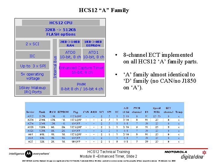
HCS 12 “A” Family HCS 12 CPU 32 KB -> 512 KB FLASH options 2 KB->14 KB RAM IIC Up to 3 x SPI 5 v operating voltage 16 key Wakeup IRQ Ports Internal Bus 2 x SCI 1 KB->4 KB EEPROM ATD 1 ATD 0 ATD 1 10 bit, 16 ch. 10 -bit, 8 ch Enhanced Capture Timer 16 -bit, 8 ch PWM 8 -bit 8 ch / 16 -bit 4 ch • 8 -channel ECT implemented on all HCS 12 ‘A’ family parts. • ‘A’ family almost identical to ‘D’ family (no CAN/no J 1850 on ‘A’). HCS 12 Technical Training Module 8 –Enhanced Timer, Slide 2 MOTOROLA and the Stylized M Logo are registered in the US Patent & Trademark Office. All other product or service names are the property of their respective owners. © Motorola, Inc. 2001.

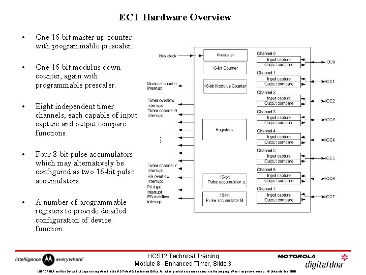
ECT Hardware Overview • One 16 -bit master up-counter with programmable prescaler. • One 16 -bit modulus downcounter, again with programmable prescaler. • Eight independent timer channels, each capable of input capture and output compare functions. • Four 8 -bit pulse accumulators which may alternatively be configured as two 16 -bit pulse accumulators. • A number of programmable registers to provide detailed configuration of device function. HCS 12 Technical Training Module 8 –Enhanced Timer, Slide 3 MOTOROLA and the Stylized M Logo are registered in the US Patent & Trademark Office. All other product or service names are the property of their respective owners. © Motorola, Inc. 2001.

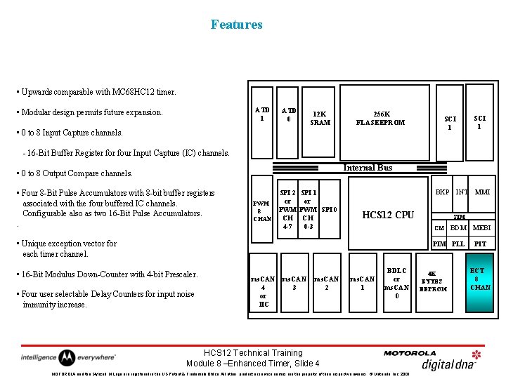
Features • Upwards comparable with MC 68 HC 12 timer. ATD 1 • Modular design permits future expansion. ATD 0 12 K SRAM 256 K FLASEEPROM SCI 1 • 0 to 8 Input Capture channels. - 16 -Bit Buffer Register four Input Capture (IC) channels. Internal Bus • 0 to 8 Output Compare channels. • Four 8 -Bit Pulse Accumulators with 8 -bit buffer registers associated with the four buffered IC channels. Configurable also as two 16 -Bit Pulse Accumulators. . SPI 2 SPI 1 or or PWM PWM SPI 0 8 CH CH CHAN 4 -7 0 -3 BKP HCS 12 CPU BDM PIM PLL • 16 -Bit Modulus Down-Counter with 4 -bit Prescaler. • Four user selectable Delay Counters for input noise immunity increase. ms. CAN 4 or IIC ms. CAN 3 ms. CAN 2 ms. CAN 1 BDLC or ms. CAN 0 HCS 12 Technical Training Module 8 –Enhanced Timer, Slide 4 MOTOROLA and the Stylized M Logo are registered in the US Patent & Trademark Office. All other product or service names are the property of their respective owners. © Motorola, Inc. 2001. MMI SIM CM • Unique exception vector for each timer channel. INT 4 K BYTES EEPROM MEBI PIT ECT 8 CHAN
![TIMER STRUCTURE PRESCALER M Clock PR2 0 FFFE FFFF 0000 1 TIMER STRUCTURE PRE-SCALER M Clock PR[2: 0] $FFFE $FFFF $0000 ******* ** **** 1](https://slidetodoc.com/presentation_image_h/77caf76e08c5d83ef479075e55a24e72/image-5.jpg)
TIMER STRUCTURE PRE-SCALER M Clock PR[2: 0] $FFFE $FFFF $0000 ******* ** **** 1 2 4 8 16 32 64 128 TCNT CLK B 0. . . . ……. . . B 7 B 8……. . B 15 15. . . 0 . TCNT TEN PIN PA DATA BUS PULSE Accumulator TSCR 1 - TIMER SYSTEM CONTROL REGISTER TEN RST: R = Reserved TOF 0 TSWAI TSFRZ TFFCA 0 0 0 R R 0 0 $0006 1 - CLOCKS COUNTER ENABLE 0 - CLOCKS COUNTER DISABLE HCS 12 Technical Training Module 8 –Enhanced Timer, Slide 5 MOTOROLA and the Stylized M Logo are registered in the US Patent & Trademark Office. All other product or service names are the property of their respective owners. © Motorola, Inc. 2001. Address Offset $0004, 05

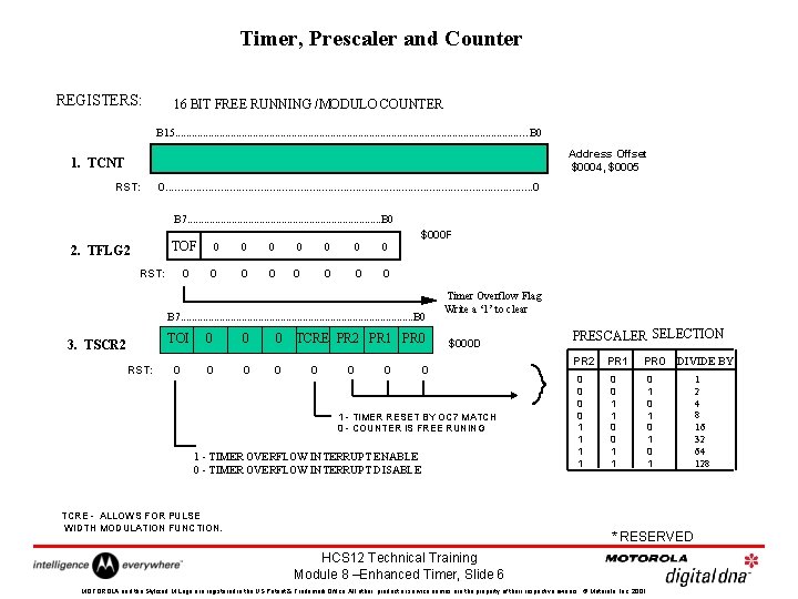
Timer, Prescaler and Counter REGISTERS: 16 BIT FREE RUNNING /MODULO COUNTER B 15. . . . . . . . …B 0 Address Offset $0004, $0005 1. TCNT RST: 0. . . . . . . . 0 B 7. . . . . B 0 2. TFLG 2 TOF 0 0 0 0 RST: $000 F B 7. . . . . . B 0 3. TSCR 2 RST: TOI 0 0 0 0 TCRE PR 2 PR 1 PR 0 0 Timer Overflow Flag Write a ‘ 1’ to clear $000 D 0 1 - TIMER RESET BY OC 7 MATCH 0 - COUNTER IS FREE RUNING 1 - TIMER OVERFLOW INTERRUPT ENABLE 0 - TIMER OVERFLOW INTERRUPT DISABLE TCRE - ALLOWS FOR PULSE WIDTH MODULATION FUNCTION. PRESCALER SELECTION PR 2 0 0 1 1 PR 1 0 0 1 1 PR 0 DIVIDE BY 0 1 0 1 * RESERVED HCS 12 Technical Training Module 8 –Enhanced Timer, Slide 6 MOTOROLA and the Stylized M Logo are registered in the US Patent & Trademark Office. All other product or service names are the property of their respective owners. © Motorola, Inc. 2001. 1 2 4 8 16 32 64 128

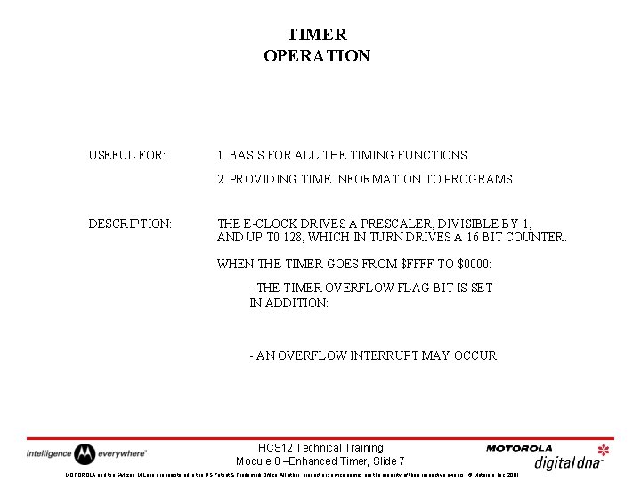
TIMER OPERATION USEFUL FOR: 1. BASIS FOR ALL THE TIMING FUNCTIONS 2. PROVIDING TIME INFORMATION TO PROGRAMS DESCRIPTION: THE E-CLOCK DRIVES A PRESCALER, DIVISIBLE BY 1, AND UP T 0 128, WHICH IN TURN DRIVES A 16 BIT COUNTER. WHEN THE TIMER GOES FROM $FFFF TO $0000: - THE TIMER OVERFLOW FLAG BIT IS SET IN ADDITION: - AN OVERFLOW INTERRUPT MAY OCCUR HCS 12 Technical Training Module 8 –Enhanced Timer, Slide 7 MOTOROLA and the Stylized M Logo are registered in the US Patent & Trademark Office. All other product or service names are the property of their respective owners. © Motorola, Inc. 2001.

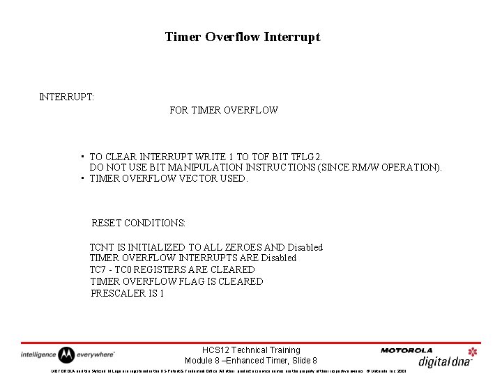
Timer Overflow Interrupt INTERRUPT: FOR TIMER OVERFLOW • TO CLEAR INTERRUPT WRITE 1 TO TOF BIT TFLG 2. DO NOT USE BIT MANIPULATION INSTRUCTIONS (SINCE RM/W OPERATION). • TIMER OVERFLOW VECTOR USED. RESET CONDITIONS: TCNT IS INITIALIZED TO ALL ZEROES AND Disabled TIMER OVERFLOW INTERRUPTS ARE Disabled TC 7 - TC 0 REGISTERS ARE CLEARED TIMER OVERFLOW FLAG IS CLEARED PRESCALER IS 1 HCS 12 Technical Training Module 8 –Enhanced Timer, Slide 8 MOTOROLA and the Stylized M Logo are registered in the US Patent & Trademark Office. All other product or service names are the property of their respective owners. © Motorola, Inc. 2001.

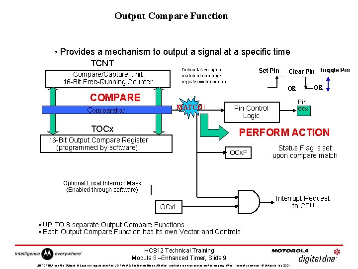
Output Compare Function • Provides a mechanism to output a signal at a specific time TCNT Action taken upon match of compare register with counter Compare/Capture Unit 16 -Bit Free-Running Counter Set Pin Clear Pin Toggle Pin OR OR COMPARE MATCH! Comparator TOCx Pin Control Logic OCx PERFORM ACTION 16 -Bit Output Compare Register (programmed by software) OCx. F Status Flag is set upon compare match Optional Local Interrupt Mask (Enabled through software) OCx. I Interrupt Request to CPU • UP TO 8 separate Output Compare Functions • Each Output Compare Function has its own Vector and Controls HCS 12 Technical Training Module 8 –Enhanced Timer, Slide 9 MOTOROLA and the Stylized M Logo are registered in the US Patent & Trademark Office. All other product or service names are the property of their respective owners. © Motorola, Inc. 2001.

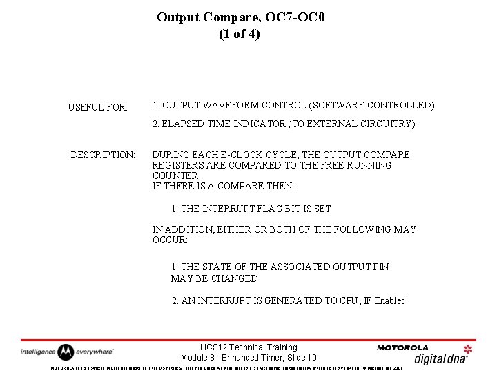
Output Compare, OC 7 -OC 0 (1 of 4) USEFUL FOR: 1. OUTPUT WAVEFORM CONTROL (SOFTWARE CONTROLLED) 2. ELAPSED TIME INDICATOR (TO EXTERNAL CIRCUITRY) DESCRIPTION: DURING EACH E-CLOCK CYCLE, THE OUTPUT COMPARE REGISTERS ARE COMPARED TO THE FREE-RUNNING COUNTER. IF THERE IS A COMPARE THEN: 1. THE INTERRUPT FLAG BIT IS SET IN ADDITION, EITHER OR BOTH OF THE FOLLOWING MAY OCCUR: 1. THE STATE OF THE ASSOCIATED OUTPUT PIN MAY BE CHANGED 2. AN INTERRUPT IS GENERATED TO CPU, IF Enabled HCS 12 Technical Training Module 8 –Enhanced Timer, Slide 10 MOTOROLA and the Stylized M Logo are registered in the US Patent & Trademark Office. All other product or service names are the property of their respective owners. © Motorola, Inc. 2001.

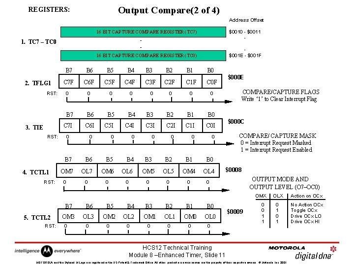
Output Compare(2 of 4) REGISTERS: Address Offset $0010 - $0011 - 16 BIT CAPTURE COMPARE REGISTER (TC 7) - 1. TC 7 – TC 0 $001 E - $001 F 16 BIT CAPTURE COMPARE REGISTER (TC 0) 2. TFLG 1 RST: 3. TIE B 7 B 6 B 5 B 4 B 3 B 2 B 1 B 0 C 7 F C 6 F C 5 F C 4 F C 3 F C 2 F C 1 F C 0 F 0 0 0 0 B 7 B 6 B 5 B 4 B 3 B 2 B 1 B 0 C 7 I C 6 I C 5 I C 4 I C 3 I C 2 I C 1 I C 0 I 0 0 0 0 B 7 B 6 B 5 B 4 OM 7 OL 7 OM 6 0 0 RST: 4. TCTL 1 RST: 0 0 B 3 B 2 B 1 B 0 OL 6 OM 5 OL 5 OM 4 OL 4 0 0 0 $000 E COMPARE/CAPTURE FLAGS Write ‘ 1’ to Clear Interrupt Flag $000 C COMPARE/ CAPTURE MASK 0 = Interrupt Request Masked 1 = Interrupt Request Enabled $0008 OUTPUT MODE AND OUTPUT LEVEL (O 7–OC 0) OMX 5. TCTL 2 RST: B 7 B 6 B 5 OM 3 OL 3 OM 2 0 0 0 B 4 B 3 B 2 B 1 B 0 OL 2 OM 1 OL 1 OM 0 OL 0 0 0 $0009 0 0 1 1 OLX Action on OCx 0 1 No Action OCx Toggle OCx Drive OCx LO Drive OCx HI HCS 12 Technical Training Module 8 –Enhanced Timer, Slide 11 MOTOROLA and the Stylized M Logo are registered in the US Patent & Trademark Office. All other product or service names are the property of their respective owners. © Motorola, Inc. 2001.

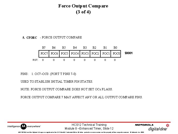
Force Output Compare (3 of 4) 5. CFORC RST: PINS: - FORCE OUTPUT COMPARE B 7 B 6 B 5 B 4 B 3 B 2 FOC 7 FOC 6 FOC 5 FOC 4 FOC 3 FOC 2 0 0 0 B 1 FOC 1 B 0 FOC 0 0 $0001 0 1. OC 7–OC 0 (PORT T PINS 7 -0) USED TO STABLISH INITIAL TIMER PIN STATES. NOTE: FORCE OUTPUT COMPARE DOES NOT SET OCx FLAGS. FORCE OUTPUT COMPARE 7 MAY AFFECT ANY OR ALL OUTPUT COMPARE PINS. HCS 12 Technical Training Module 8 –Enhanced Timer, Slide 12 MOTOROLA and the Stylized M Logo are registered in the US Patent & Trademark Office. All other product or service names are the property of their respective owners. © Motorola, Inc. 2001.

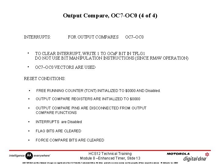
Output Compare, OC 7 -OC 0 (4 of 4) INTERRUPTS: FOR OUTPUT COMPARES OC 7–OC 0 • TO CLEAR INTERRUPT, WRITE 1 TO OCx. F BIT IN TFLG 1 DO NOT USE BIT MANIPULATION INSTRUCTIONS (SINCE RM/W OPERATION) • OC 7–OC 0 VECTORS ARE USED RESET CONDITIONS: • FREE RUNNING COUNTER (TCNT) INITIALIZED TO $0000 AND Disabled. • OUTPUT COMPARE REGISTERS ARE INITIALIZED TO $0000 • OUTPUT COMPARE PINS ARE DISCONNECTED FROM OUTPUT COMPARE FUNCTIONS • INTERRUPTS are Disabled • FLAG BITS ARE CLEARED • FORCE COMPARE BITS ARE CLEARED HCS 12 Technical Training Module 8 –Enhanced Timer, Slide 13 MOTOROLA and the Stylized M Logo are registered in the US Patent & Trademark Office. All other product or service names are the property of their respective owners. © Motorola, Inc. 2001.

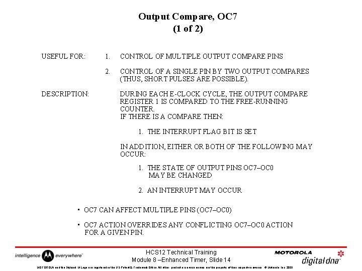
Output Compare, OC 7 (1 of 2) USEFUL FOR: DESCRIPTION: 1. CONTROL OF MULTIPLE OUTPUT COMPARE PINS 2. CONTROL OF A SINGLE PIN BY TWO OUTPUT COMPARES (THUS, SHORT PULSES ARE POSSIBLE). DURING EACH E-CLOCK CYCLE, THE OUTPUT COMPARE REGISTER 1 IS COMPARED TO THE FREE-RUNNING COUNTER. IF THERE IS A COMPARE THEN: 1. THE INTERRUPT FLAG BIT IS SET IN ADDITION, EITHER OR BOTH OF THE FOLLOWING MAY OCCUR: 1. THE STATE OF OUTPUT PINS OC 7–OC 0 MAY BE CHANGED 2. AN INTERRUPT MAY OCCUR • OC 7 CAN AFFECT MULTIPLE PINS (OC 7–OC 0) • OC 7 ACTION OVERRIDES ANY CONFLICTING OC 7–OC 0 ACTION FOR A GIVEN PIN. HCS 12 Technical Training Module 8 –Enhanced Timer, Slide 14 MOTOROLA and the Stylized M Logo are registered in the US Patent & Trademark Office. All other product or service names are the property of their respective owners. © Motorola, Inc. 2001.

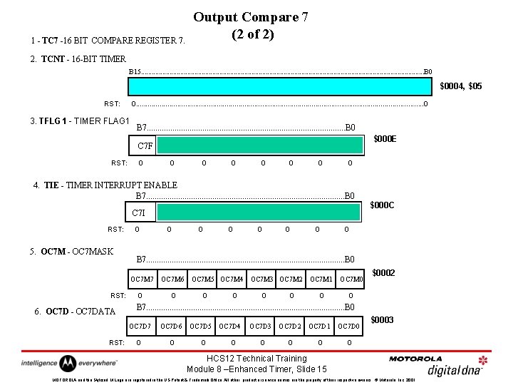
1 - TC 7 -16 BIT COMPARE REGISTER 7. Output Compare 7 (2 of 2) 2. TCNT - 16 -BIT TIMER B 15. . . . . . . . . . B 0 $0004, $05 RST: 0. . . . . . . . . 0 3. TFLG 1 - TIMER FLAG 1 B 7. . . . . . B 0 C 7 F RST: 0 C 6 F 0 C 5 F C 4 F C 3 F C 2 F 0 0 C 1 F C 0 F 0 0 4. TIE - TIMER INTERRUPT ENABLE B 7. . . . . . B 0 RST: 5. OC 7 M - OC 7 MASK C 7 I C 6 F 0 0 6. OC 7 D - OC 7 DATA RST: C 4 F C 3 F C 2 F 0 0 C 1 F C 0 F 0 0 $000 C B 7. . . . . . B 0 OC 7 M 7 OC 7 M 6 RST: C 5 F $000 E 0 0 OC 7 M 5 OC 7 M 4 0 0 OC 7 M 3 OC 7 M 2 0 0 OC 7 M 1 OC 7 M 0 0 0 $0002 B 7. . . . . . B 0 OC 7 D 7 OC 7 D 6 0 0 OC 7 D 5 0 OC 7 D 4 0 OC 7 D 3 0 OC 7 D 2 OC 7 D 1 OC 7 D 0 0 $0003 HCS 12 Technical Training Module 8 –Enhanced Timer, Slide 15 MOTOROLA and the Stylized M Logo are registered in the US Patent & Trademark Office. All other product or service names are the property of their respective owners. © Motorola, Inc. 2001.

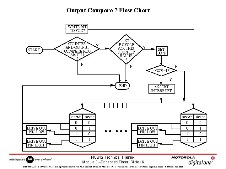
Output Compare 7 Flow Chart WRITE BIT TO FOC 7 START COUNTER AND OUTPUT COMPARE REG MATCH ? N Y 1 ST E CYCLE FOR THIS COUNTER VALUE ? Y SET OC 7 F N N OC 7 I=1? Y END DRIVE OC 0 PIN LOW DRIVE OC 0 PIN HIGH ASSERT INTERRUPT OC 7 M 0 OC 7 D 0 OC 7 M 7 OC 7 D 7 0 0 1 1 0 1 0 1 • • • DRIVE OC 7 PIN LOW DRIVE OC 7 PIN HIGH HCS 12 Technical Training Module 8 –Enhanced Timer, Slide 16 MOTOROLA and the Stylized M Logo are registered in the US Patent & Trademark Office. All other product or service names are the property of their respective owners. © Motorola, Inc. 2001.

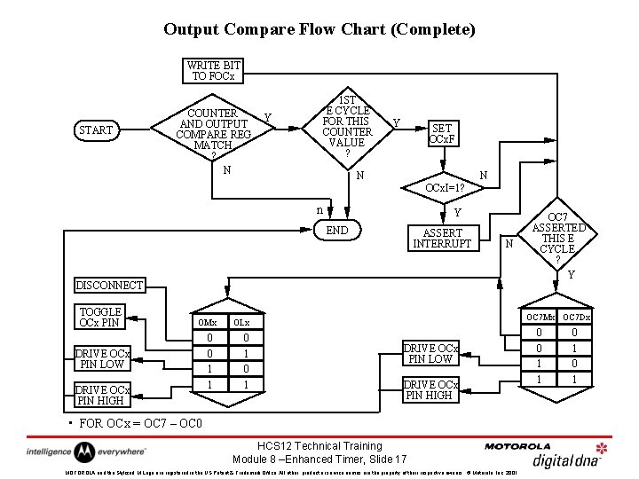
Output Compare Flow Chart (Complete) WRITE BIT TO FOCx START COUNTER AND OUTPUT COMPARE REG MATCH ? N 1 ST E CYCLE FOR THIS COUNTER VALUE ? Y Y SET OCx. F N N OCx. I=1? n Y END ASSERT INTERRUPT N DISCONNECT TOGGLE OCx PIN OMx DRIVE OCx PIN LOW DRIVE OCx PIN HIGH 0 0 1 1 OC 7 Mx OC 7 Dx OLx 0 1 OC 7 ASSERTED THIS E CYCLE ? Y DRIVE OCx PIN LOW DRIVE OCx PIN HIGH • FOR OCx = OC 7 – OC 0 HCS 12 Technical Training Module 8 –Enhanced Timer, Slide 17 MOTOROLA and the Stylized M Logo are registered in the US Patent & Trademark Office. All other product or service names are the property of their respective owners. © Motorola, Inc. 2001. 0 0 1 1 0 1

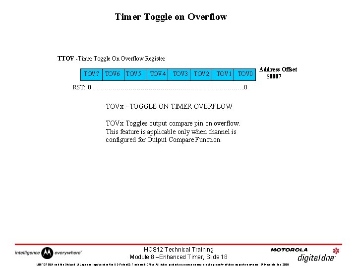
Timer Toggle on Overflow TTOV -Timer Toggle On Overflow Register TOV 7 TOV 6 TOV 5 TOV 4 TOV 3 TOV 2 TOV 1 TOV 0 Address Offset $0007 RST: 0………………………………. …. . 0 TOVx - TOGGLE ON TIMER OVERFLOW TOVx Toggles output compare pin on overflow. This feature is applicable only when channel is configured for Output Compare Function. HCS 12 Technical Training Module 8 –Enhanced Timer, Slide 18 MOTOROLA and the Stylized M Logo are registered in the US Patent & Trademark Office. All other product or service names are the property of their respective owners. © Motorola, Inc. 2001.

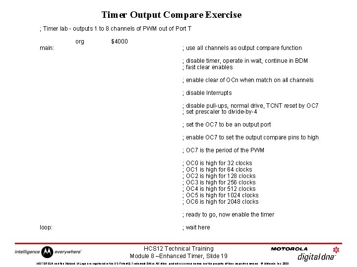
Timer Output Compare Exercise ; Timer lab - outputs 1 to 8 channels of PWM out of Port T main: org $4000 ; use all channels as output compare function ; disable timer, operate in wait, continue in BDM ; fast clear enables ; enable clear of OCn when match on all channels ; disable Interrupts ; disable pull-ups, normal drive, TCNT reset by OC 7 ; set prescaler to divide-by-4 ; set the OC 7 to be an output port ; enable OC 7 to set the output compare pins to high ; OC 7 is the period of the PWM ; OC 0 is high for 32 clocks ; OC 1 is high for 64 clocks ; OC 2 is high for 128 clocks ; OC 3 is high for 256 clocks ; OC 4 is high for 512 clocks ; OC 5 is high for 1024 clocks ; OC 6 is high for 2048 clocks ; ready to go, now enable the timer loop: ; wait here HCS 12 Technical Training Module 8 –Enhanced Timer, Slide 19 MOTOROLA and the Stylized M Logo are registered in the US Patent & Trademark Office. All other product or service names are the property of their respective owners. © Motorola, Inc. 2001.

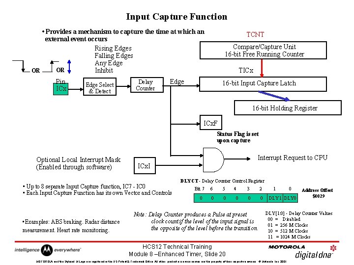
Input Capture Function • Provides a mechanism to capture the time at which an external event occurs Rising Edges Falling Edges Any Edge OR Inhibit OR Pin ICx Edge Select & Detect Delay Counter TCNT Compare/Capture Unit 16 -bit Free Running Counter TICx Edge 16 -bit Input Capture Latch 16 -bit Holding Register ICx. F Status Flag is set upon capture Optional Local Interrupt Mask (Enabled through software) Interrupt Request to CPU ICx. I • Up to 8 separate Input Capture function, IC 7 - IC 0 • Each Input Capture Function has its own Vector and Controls • Examples: ABS braking. Radar distance measurement. Heart rate monitoring. DLYCT - Delay Counter Control Register Bit 7 0 6 5 0 0 4 0 3 2 0 0 Note: Delay Counter produces a Pulse at preset clock count if the level of the input signal is the opposite of the level before the transition. 1 0 DLY 1 DLY 0 Address Offset $0029 DLY[1: 0] - Delay Counter Values 00 = Disabled 01 = 256 M Clocks 10 = 512 M Clocks 11 = 1024 M Clocks HCS 12 Technical Training Module 8 –Enhanced Timer, Slide 20 MOTOROLA and the Stylized M Logo are registered in the US Patent & Trademark Office. All other product or service names are the property of their respective owners. © Motorola, Inc. 2001.

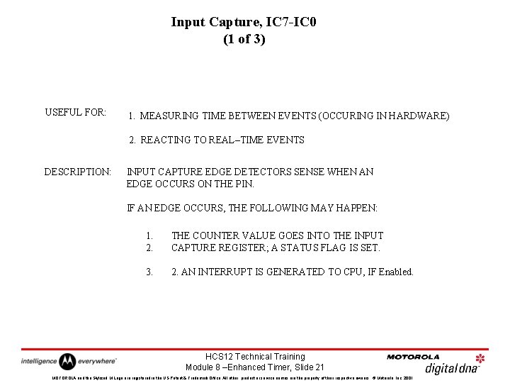
Input Capture, IC 7 -IC 0 (1 of 3) USEFUL FOR: 1. MEASURING TIME BETWEEN EVENTS (OCCURING IN HARDWARE) 2. REACTING TO REAL–TIME EVENTS DESCRIPTION: INPUT CAPTURE EDGE DETECTORS SENSE WHEN AN EDGE OCCURS ON THE PIN. IF AN EDGE OCCURS, THE FOLLOWING MAY HAPPEN: 1. 2. THE COUNTER VALUE GOES INTO THE INPUT CAPTURE REGISTER; A STATUS FLAG IS SET. 3. 2. AN INTERRUPT IS GENERATED TO CPU, IF Enabled. HCS 12 Technical Training Module 8 –Enhanced Timer, Slide 21 MOTOROLA and the Stylized M Logo are registered in the US Patent & Trademark Office. All other product or service names are the property of their respective owners. © Motorola, Inc. 2001.

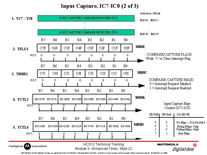
Input Capture, IC 7 -IC 0 (2 of 3) Address Offset 16 BIT CAPTURE COMPARE REGISTER (TC 7) 1. TC 7 – TC 0 $0010 - $0011 - - $001 E - $001 F 16 BIT CAPTURE COMPARE REGISTER (TC 0) 2. TFLG 1 B 7 B 6 B 5 B 4 C 7 F C 6 F C 5 F C 4 F RST: 3. TMSK 1 0 B 7 0 0 B 6 B 5 B 4 C 7 I C 6 I C 5 I 0 0 0 B 7 4. TCTL 3 RST: B 6 EDG 7 B EDG 7 A 0 0 B 5 B 2 B 1 C 3 F B 1 C 2 F B 0 C 1 F B 2 0 RST: 0 B 3 B 0 C 0 F 0 0 B 3 B 2 B 1 B 0 C 4 I C 3 I C 2 I C 1 I C 0 I 0 0 B 4 B 3 0 B 2 B 1 0 0 COMPARE/CAPTURE FLAGS Write ‘ 1’ to Clear Interrupt Flag 0 $000 C COMPARE/ CAPTURE MASK 0 = Interrupt Request Masked 1 = Interrupt Request Enabled B 0 EDG 6 B EDG 6 A EDG 5 B EDG 5 A EDG 4 B EDG 4 A 0 $000 E $000 A Input Capture Edge Control (IC 7–IC 0) 0 EDGx. B B 7 5. TCTL 4 RST: EDG 3 B 0 B 6 B 5 B 4 B 3 B 2 EDG 3 A EDG 2 B EDG 2 A EDG 1 B EDG 1 A 0 0 0 B 1 ICx EDGE B 0 EDG 0 B EDG 0 A 0 EDGx. A 0 $000 B 0 0 1 1 0 1 HCS 12 Technical Training Module 8 –Enhanced Timer, Slide 22 MOTOROLA and the Stylized M Logo are registered in the US Patent & Trademark Office. All other product or service names are the property of their respective owners. © Motorola, Inc. 2001. No Edge – ICx Disabled Rising Edges Only Falling Edges Only Any Edge

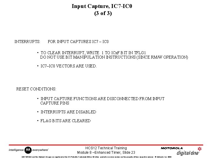
Input Capture, IC 7 -IC 0 (3 of 3) INTERRUPTS: FOR INPUT CAPTURES IC 7 – IC 0 • TO CLEAR INTERRUPT, WRITE 1 TO ICx. F BIT IN TFLG 1 DO NOT USE BIT MANIPULATION INSTRUCTIONS (SINCE RM/W OPERATION) • IC 7–IC 0 VECTORS ARE USED. RESET CONDITIONS: • INPUT CAPTURE FUNCTIONS ARE DISCONNECTED FROM INPUT CAPTURE PINS • INTERRUPTS ARE DISABLED • FLAG BITS ARE CLEARED HCS 12 Technical Training Module 8 –Enhanced Timer, Slide 23 MOTOROLA and the Stylized M Logo are registered in the US Patent & Trademark Office. All other product or service names are the property of their respective owners. © Motorola, Inc. 2001.

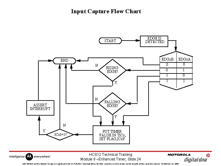
Input Capture Flow Chart START END N RISING EDGE? Y N ASSERT INTERRUPT EDGE IS DETECTED EDGx. B 0 0 1 EDGx. A 0 1 1 FALLING EDGE? Y N Y ICx. I=1? PUT TIMER VALUE IN TICx; SET FLAG, ICx. F HCS 12 Technical Training Module 8 –Enhanced Timer, Slide 24 MOTOROLA and the Stylized M Logo are registered in the US Patent & Trademark Office. All other product or service names are the property of their respective owners. © Motorola, Inc. 2001. 1 0

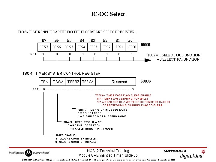
IC/OC Select TIOS - TIMER INPUT CAPTURE/OUTPUT COMPARE SELECT REGISTER RST: B 7 B 6 B 5 B 4 B 3 IOS 7 IOS 6 IOS 5 IOS 4 IOS 3 0 0 0 B 2 B 1 B 0 IOS 2 IOS 1 IOS 0 0 $0000 IOSx = 1 SELECT OC FUNCTION = 0 SELECT IC FUNCTION TSCR - TIMER SYSTEM CONTROL REGISTER TEN RST: TSWAI TSFRZ TFFCA Reserved $0006 0……………………………………… 0 TFFCA - TIMER FAST FLAG CLEAR ENABLE 0 = TIMER FLAG CLEARING NORMALLY 1 = A READ FOR IC, A WRITE OF OC REGISTER CAUSES CORRESPONDING CHANNEL FLAG TO CLEAR TSBCK - TIMER STOP IN DEBUG MODE 0 = DO NOT STOP 1 = DISABLE TIMER IN DEBUG MODE TSWAI - TIMER STOP IN WAIT 0 = NORMAL OPERATION 1 = DISABLE TIMER IN WAIT MODE TIMER ENABLE 1 - CLOCKS COUNTER ENABLE 0 - CLOCKS COUNTER DISABLE HCS 12 Technical Training Module 8 –Enhanced Timer, Slide 25 MOTOROLA and the Stylized M Logo are registered in the US Patent & Trademark Office. All other product or service names are the property of their respective owners. © Motorola, Inc. 2001.

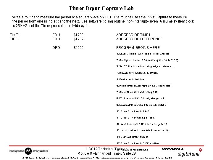
Timer Input Capture Lab Write a routine to measure the period of a square wave on TC 1. The routine uses the Input Capture to measure the period from one rising edge to the next. Use software polling routine, non-Interrupt-driven. Assume system clock is 25 MHZ, set the Timer prescaler to divide by 4. TIME 1 DIFF EQU $1200 $1202 ADDRESS OF TIME 1 ADDRESS OF DIFFERENCE ORG $4000 PROGRAM BEGINS HERE 1. Load X register with register block address 2. Configure channel 1 for input capture (write TIOS) 3. Set TCTL 4 to capture rising edge on channel 1. 4. Disable Ch 1 Interrupts in TMSK 2 5. Enable and start timer 6. Read Timer status register into Accumulator 7. Clear Timer Ch 1 status flag C 1 F. 8. Wait here until C 1 F is set, else go to 9. 9. Load captured value into Accumulator D. 10. Store D to Ram in TIME 1 11. Clear C 1 F by writing a 1 to it 12. Wait here until C 1 F is set, else go to 13. Load captured value into Accumulator D. 14. Subtract TIME 1 from D 15. Store D to Ram in DIFF location. HCS 12 Technical Training 16. Return from subroutine Module 8 –Enhanced Timer, Slide 26 MOTOROLA and the Stylized M Logo are registered in the US Patent & Trademark Office. All other product or service names are the property of their respective owners. © Motorola, Inc. 2001.

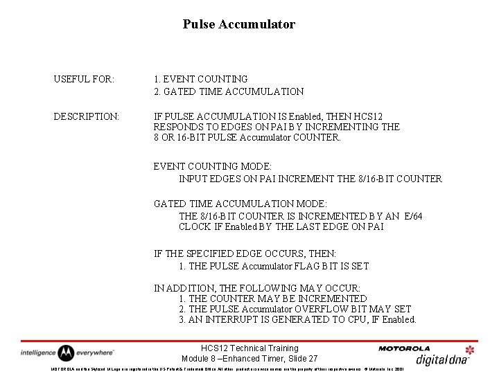
Pulse Accumulator USEFUL FOR: 1. EVENT COUNTING 2. GATED TIME ACCUMULATION DESCRIPTION: IF PULSE ACCUMULATION IS Enabled, THEN HCS 12 RESPONDS TO EDGES ON PAI BY INCREMENTING THE 8 OR 16 -BIT PULSE Accumulator COUNTER. EVENT COUNTING MODE: INPUT EDGES ON PAI INCREMENT THE 8/16 -BIT COUNTER GATED TIME ACCUMULATION MODE: THE 8/16 -BIT COUNTER IS INCREMENTED BY AN E/64 CLOCK IF Enabled BY THE LAST EDGE ON PAI IF THE SPECIFIED EDGE OCCURS, THEN: 1. THE PULSE Accumulator FLAG BIT IS SET IN ADDITION, THE FOLLOWING MAY OCCUR: 1. THE COUNTER MAY BE INCREMENTED 2. THE PULSE Accumulator OVERFLOW BIT MAY SET 3. AN INTERRUPT IS GENERATED TO CPU, IF Enabled. HCS 12 Technical Training Module 8 –Enhanced Timer, Slide 27 MOTOROLA and the Stylized M Logo are registered in the US Patent & Trademark Office. All other product or service names are the property of their respective owners. © Motorola, Inc. 2001.

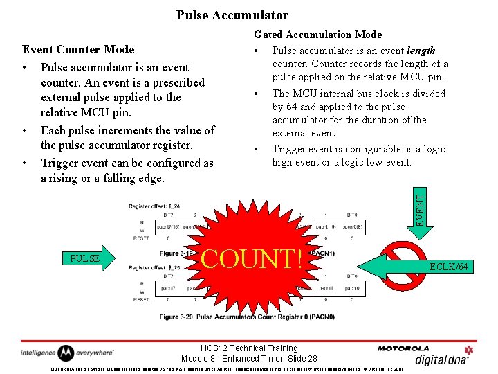
Pulse Accumulator EVENT Event Counter Mode • Pulse accumulator is an event counter. An event is a prescribed external pulse applied to the relative MCU pin. • Each pulse increments the value of the pulse accumulator register. • Trigger event can be configured as a rising or a falling edge. Gated Accumulation Mode • Pulse accumulator is an event length counter. Counter records the length of a pulse applied on the relative MCU pin. • The MCU internal bus clock is divided by 64 and applied to the pulse accumulator for the duration of the external event. • Trigger event is configurable as a logic high event or a logic low event. PULSE COUNT! +1 HCS 12 Technical Training Module 8 –Enhanced Timer, Slide 28 MOTOROLA and the Stylized M Logo are registered in the US Patent & Trademark Office. All other product or service names are the property of their respective owners. © Motorola, Inc. 2001. ECLK/64

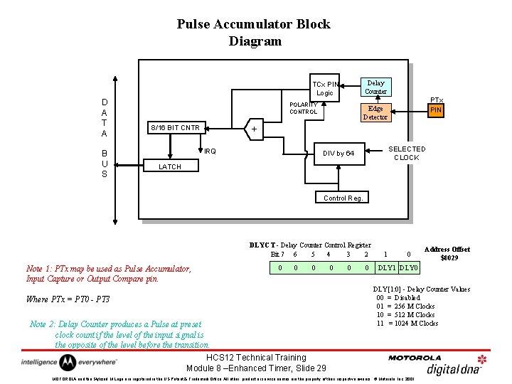
Pulse Accumulator Block Diagram Delay Counter TCx PIN Logic D A T A B U S POLARITY CONTROL PTx PIN Edge Detector + 8/16 BIT CNTR IRQ SELECTED CLOCK DIV by 64 LATCH Control Reg. DLYCT - Delay Counter Control Register Bit 7 6 5 4 3 2 Note 1: PTx may be used as Pulse Accumulator, Input Capture or Output Compare pin. 0 0 0 Where PTx = PT 0 - PT 3 Note 2: Delay Counter produces a Pulse at preset clock count if the level of the input signal is the opposite of the level before the transition. 0 0 0 1 0 Address Offset $0029 DLY 1 DLY 0 DLY[1: 0] - Delay Counter Values 00 = Disabled 01 = 256 M Clocks 10 = 512 M Clocks 11 = 1024 M Clocks HCS 12 Technical Training Module 8 –Enhanced Timer, Slide 29 MOTOROLA and the Stylized M Logo are registered in the US Patent & Trademark Office. All other product or service names are the property of their respective owners. © Motorola, Inc. 2001.

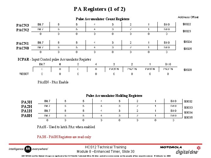
PA Registers (1 of 2) Pulse Accumulator Count Registers Address Offset PACN 3 PACN 2 $0022 PACN 1 PACN 0 $0024 $0023 $0025 ICPAR - Input Control pulse Accumulator Register $0028 PAx. EN - PAx Enable Pulse Accumulator Holding Registers $0032 PA 3 H PA 2 H PA 1 H PA 0 H $0033 $0034 $0035 PAx. H - Used to latch PAx when enabled PA 3 H - PA 0 H Registers are read only HCS 12 Technical Training Module 8 –Enhanced Timer, Slide 30 MOTOROLA and the Stylized M Logo are registered in the US Patent & Trademark Office. All other product or service names are the property of their respective owners. © Motorola, Inc. 2001.

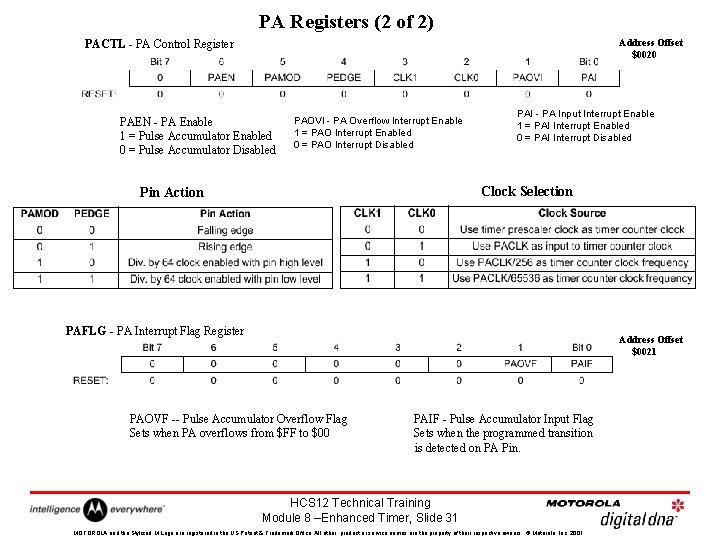
PA Registers (2 of 2) Address Offset $0020 PACTL - PA Control Register PAEN - PA Enable 1 = Pulse Accumulator Enabled 0 = Pulse Accumulator Disabled PAOVI - PA Overflow Interrupt Enable 1 = PAO Interrupt Enabled 0 = PAO Interrupt Disabled PAI - PA Input Interrupt Enable 1 = PAI Interrupt Enabled 0 = PAI Interrupt Disabled Clock Selection Pin Action PAFLG - PA Interrupt Flag Register Address Offset $0021 PAOVF -- Pulse Accumulator Overflow Flag Sets when PA overflows from $FF to $00 PAIF - Pulse Accumulator Input Flag Sets when the programmed transition is detected on PA Pin. HCS 12 Technical Training Module 8 –Enhanced Timer, Slide 31 MOTOROLA and the Stylized M Logo are registered in the US Patent & Trademark Office. All other product or service names are the property of their respective owners. © Motorola, Inc. 2001.

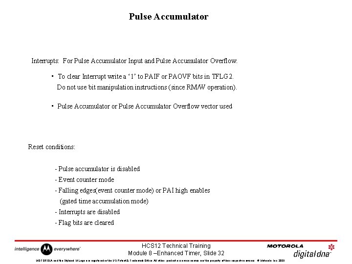
Pulse Accumulator Interrupts: For Pulse Accumulator Input and Pulse Accumulator Overflow. • To clear Interrupt write a ‘ 1’ to PAIF or PAOVF bits in TFLG 2. Do not use bit manipulation instructions (since RM/W operation). • Pulse Accumulator or Pulse Accumulator Overflow vector used Reset conditions: - Pulse accumulator is disabled - Event counter mode - Falling edges(event counter mode) or PAI high enables (gated time accumulation mode) - Interrupts are disabled - Flag bits are cleared HCS 12 Technical Training Module 8 –Enhanced Timer, Slide 32 MOTOROLA and the Stylized M Logo are registered in the US Patent & Trademark Office. All other product or service names are the property of their respective owners. © Motorola, Inc. 2001.

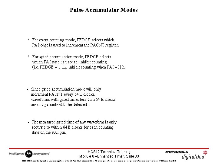
Pulse Accumulator Modes • For event counting mode, PEDGE selects which PAI edge is used to increment the PACNT register. • For gated accumulation mode, PEDGE selects which PAI state is used to inhibit counting. (i. e. PEDGE = 1 inhibit counting when PAI = HI). • Since gated accumulation mode will only increment PACNT every 64 E clocks, waveforms with gated times less than 64 E clocks are not guaranteed to be detected. • The measured gated time of any waveform is only accurate to within 64 E clocks for each counting state on the PAI pin. HCS 12 Technical Training Module 8 –Enhanced Timer, Slide 33 MOTOROLA and the Stylized M Logo are registered in the US Patent & Trademark Office. All other product or service names are the property of their respective owners. © Motorola, Inc. 2001.

ECT Latch & Queue Modes HCS 12 Technical Training Module 8 –Enhanced Timer, Slide 34 MOTOROLA and the Stylized M Logo are registered in the US Patent & Trademark Office. All other product or service names are the property of their respective owners. © Motorola, Inc. 2001.

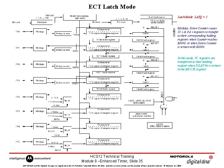
ECT Latch Mode: LATQ = 1 Modulus Down-Counter causes IC x & PA x registers to transfer to their corresponding holding registers when Counter reaches $0000, or when Down-Counter is written with $0000. . In this mode, IC registers are transferred to their holding register when ICLAT bit is written in the MCCTL register HCS 12 Technical Training Module 8 –Enhanced Timer, Slide 35 MOTOROLA and the Stylized M Logo are registered in the US Patent & Trademark Office. All other product or service names are the property of their respective owners. © Motorola, Inc. 2001.

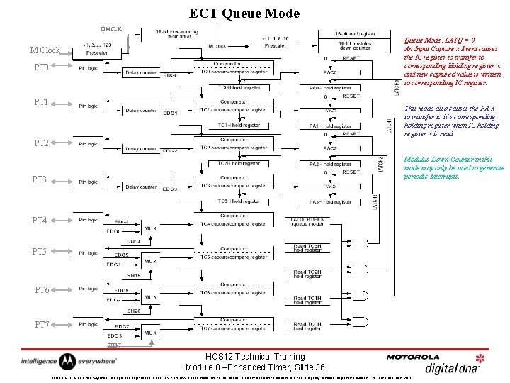
ECT Queue Mode TIMCLK Queue Mode: LATQ = 0 An Input Capture x Event causes the IC register to transfer to corresponding Holding register x, and new captured value is written to corresponding IC register. M Clock PT 0 PT 1 This mode also causes the PA x to transfer to it’s corresponding holding register when IC holding register x is read. PT 2 Modulus Down-Counter in this mode may only be used to generate periodic Interrupts. PT 3 PT 4 PT 5 PT 6 PT 7 SH 37 HCS 12 Technical Training Module 8 –Enhanced Timer, Slide 36 MOTOROLA and the Stylized M Logo are registered in the US Patent & Trademark Office. All other product or service names are the property of their respective owners. © Motorola, Inc. 2001.

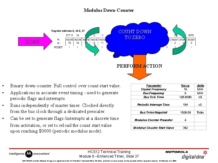
Modulus Down-Counter LOAD COUNT DOWN TO ZERO PERFORM ACTION • • Binary down-counter. Full control over count start value. Applications in accurate event timing - used to generate periodic flags and interrupts. Runs independently of master timer. Clocked directly from the bus clock through a dedicated prescaler. Can be set to generate flags /interrupts at a discrete time from activation, or set to reload the count start value upon reaching $0000 (periodic modulus mode). HCS 12 Technical Training Module 8 –Enhanced Timer, Slide 37 MOTOROLA and the Stylized M Logo are registered in the US Patent & Trademark Office. All other product or service names are the property of their respective owners. © Motorola, Inc. 2001.

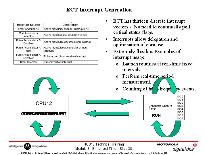
ECT Interrupt Generation • • • ECT has thirteen discrete interrupt vectors - No need to continually poll critical status flags. Interrupts allow delegation and optimisation of core use. Extremely flexible. Examples of interrupt usage: o Launch routines at real-time fixed intervals. o Perform real-time period measurement. o Counting of high-frequency events. CORE PROCESS SETUNUSED UP INTERRUPT BY ECT RUN HCS 12 Technical Training Module 8 –Enhanced Timer, Slide 38 MOTOROLA and the Stylized M Logo are registered in the US Patent & Trademark Office. All other product or service names are the property of their respective owners. © Motorola, Inc. 2001.

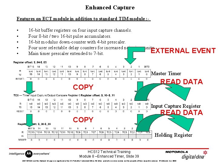
Enhanced Capture Features on ECT module in addition to standard TIM module : - • • • 16 -bit buffer registers on four input capture channels. Four 8 -bit / two 16 -bit pulse accumulators. 16 -bit modulus down-counter with 4 -bit prescaler. Four user selectable delay counters for increased noise immunity. EXTERNAL Main timer prescaler extended to 7 -bit. EVENT Master Timer COPY READ DATA Input Capture Register COPY READ DATA Holding Register HCS 12 Technical Training Module 8 –Enhanced Timer, Slide 39 MOTOROLA and the Stylized M Logo are registered in the US Patent & Trademark Office. All other product or service names are the property of their respective owners. © Motorola, Inc. 2001.

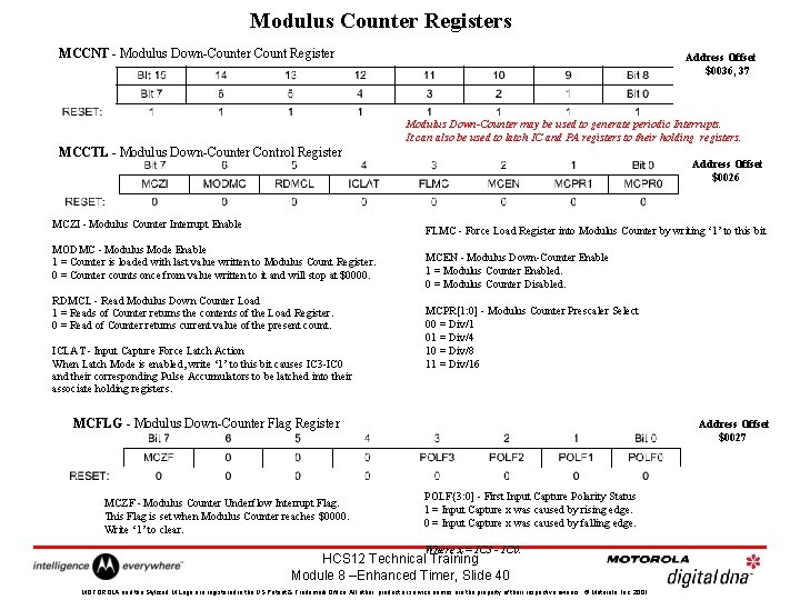
Modulus Counter Registers MCCNT - Modulus Down-Counter Count Register Address Offset $0036, 37 Modulus Down-Counter may be used to generate periodic Interrupts. It can also be used to latch IC and PA registers to their holding registers. MCCTL - Modulus Down-Counter Control Register MCZI - Modulus Counter Interrupt Enable Address Offset $0026 FLMC - Force Load Register into Modulus Counter by writing ‘ 1’ to this bit MODMC - Modulus Mode Enable 1 = Counter is loaded with last value written to Modulus Count Register. 0 = Counter counts once from value written to it and will stop at $0000. RDMCL - Read Modulus Down Counter Load 1 = Reads of Counter returns the contents of the Load Register. 0 = Read of Counter returns current value of the present count. ICLAT - Input Capture Force Latch Action When Latch Mode is enabled, write ‘ 1’ to this bit causes IC 3 -IC 0 and their corresponding Pulse Accumulators to be latched into their associate holding registers. MCEN - Modulus Down-Counter Enable 1 = Modulus Counter Enabled. 0 = Modulus Counter Disabled. MCPR[1: 0] - Modulus Counter Prescaler Select 00 = Div/1 01 = Div/4 10 = Div/8 11 = Div/16 MCFLG - Modulus Down-Counter Flag Register MCZF - Modulus Counter Underflow Interrupt Flag. This Flag is set when Modulus Counter reaches $0000. Write ‘ 1’ to clear. Address Offset $0027 POLF{3: 0] - First Input Capture Polarity Status 1 = Input Capture x was caused by rising edge. 0 = Input Capture x was caused by falling edge. Where x = IC 3 - IC 0. HCS 12 Technical Training Module 8 –Enhanced Timer, Slide 40 MOTOROLA and the Stylized M Logo are registered in the US Patent & Trademark Office. All other product or service names are the property of their respective owners. © Motorola, Inc. 2001.

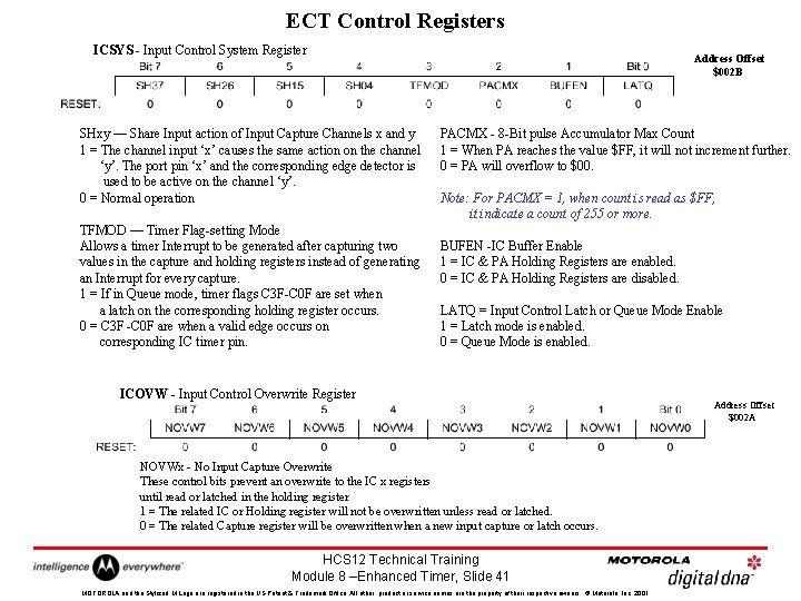
ECT Control Registers ICSYS - Input Control System Register SHxy — Share Input action of Input Capture Channels x and y 1 = The channel input ‘x’ causes the same action on the channel ‘y’. The port pin ‘x’ and the corresponding edge detector is used to be active on the channel ‘y’. 0 = Normal operation TFMOD — Timer Flag-setting Mode Allows a timer Interrupt to be generated after capturing two values in the capture and holding registers instead of generating an Interrupt for every capture. 1 = If in Queue mode, timer flags C 3 F-C 0 F are set when a latch on the corresponding holding register occurs. 0 = C 3 F -C 0 F are when a valid edge occurs on corresponding IC timer pin. Address Offset $002 B PACMX - 8 -Bit pulse Accumulator Max Count 1 = When PA reaches the value $FF, it will not increment further. 0 = PA will overflow to $00. Note: For PACMX = 1, when count is read as $FF, it indicate a count of 255 or more. BUFEN -IC Buffer Enable 1 = IC & PA Holding Registers are enabled. 0 = IC & PA Holding Registers are disabled. LATQ = Input Control Latch or Queue Mode Enable 1 = Latch mode is enabled. 0 = Queue Mode is enabled. ICOVW - Input Control Overwrite Register NOVWx - No Input Capture Overwrite These control bits prevent an overwrite to the IC x registers until read or latched in the holding register 1 = The related IC or Holding register will not be overwritten unless read or latched. 0 = The related Capture register will be overwritten when a new input capture or latch occurs. HCS 12 Technical Training Module 8 –Enhanced Timer, Slide 41 MOTOROLA and the Stylized M Logo are registered in the US Patent & Trademark Office. All other product or service names are the property of their respective owners. © Motorola, Inc. 2001. Address Offset $002 A

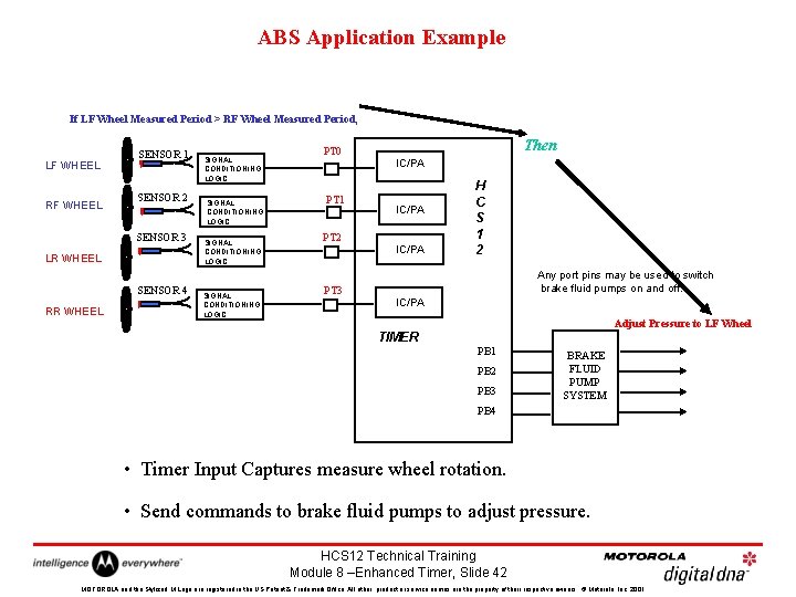
ABS Application Example If LF Wheel Measured Period > RF Wheel Measured Period, LF WHEEL RF WHEEL SENSOR 1 SENSOR 2 SENSOR 3 LR WHEEL SENSOR 4 RR WHEEL SIGNAL CONDITIONING LOGIC PT 0 PT 1 Then IC/PA PT 2 IC/PA H C S 1 2 Any port pins may be used to switch brake fluid pumps on and off. PT 3 IC/PA TIMER Adjust Pressure to LF Wheel PB 1 PB 2 PB 3 BRAKE FLUID PUMP SYSTEM PB 4 • Timer Input Captures measure wheel rotation. • Send commands to brake fluid pumps to adjust pressure. HCS 12 Technical Training Module 8 –Enhanced Timer, Slide 42 MOTOROLA and the Stylized M Logo are registered in the US Patent & Trademark Office. All other product or service names are the property of their respective owners. © Motorola, Inc. 2001.

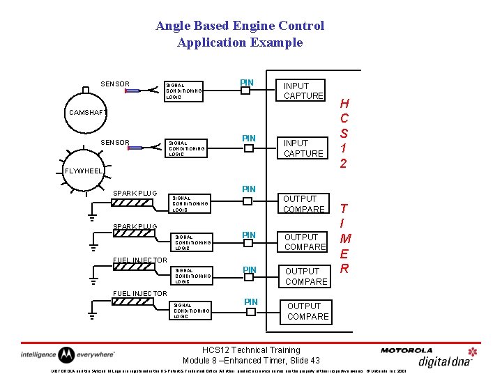
Angle Based Engine Control Application Example SENSOR SIGNAL CONDITIONING LOGIC PIN INPUT CAPTURE CAMSHAFT SENSOR SIGNAL CONDITIONING LOGIC PIN INPUT CAPTURE FLYWHEEL SPARK PLUG H C S 1 2 PIN OUTPUT COMPARE SIGNAL CONDITIONING LOGIC SPARK PLUG SIGNAL CONDITIONING LOGIC PIN OUTPUT COMPARE FUEL INJECTOR SIGNAL CONDITIONING LOGIC T I M E R FUEL INJECTOR SIGNAL CONDITIONING LOGIC HCS 12 Technical Training Module 8 –Enhanced Timer, Slide 43 MOTOROLA and the Stylized M Logo are registered in the US Patent & Trademark Office. All other product or service names are the property of their respective owners. © Motorola, Inc. 2001.

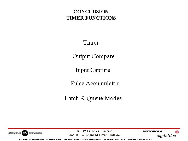
CONCLUSION TIMER FUNCTIONS Timer Output Compare Input Capture Pulse Accumulator Latch & Queue Modes HCS 12 Technical Training Module 8 –Enhanced Timer, Slide 44 MOTOROLA and the Stylized M Logo are registered in the US Patent & Trademark Office. All other product or service names are the property of their respective owners. © Motorola, Inc. 2001.