Chapter 9 Serial Communication Interface SCI Why Serial

- Slides: 49

Chapter 9 Serial Communication Interface SCI

Why Serial Communication? • Parallel data transfer requires many I/O pins. This requirement prevents the microcontroller from interfacing with as many devices as desired in the application. • Many I/O devices do not have high data rate to justify the use of parallel data transfer. • Data synchronization for parallel transfer is difficult to achieve over a long distance. This requirement is one of the reasons that data communications are always using serial transfer. • Consider cost.

What is SCI? • An interface designed to transfer data only in asynchronous mode that utilizes the EIA-232 standard.

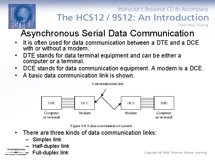
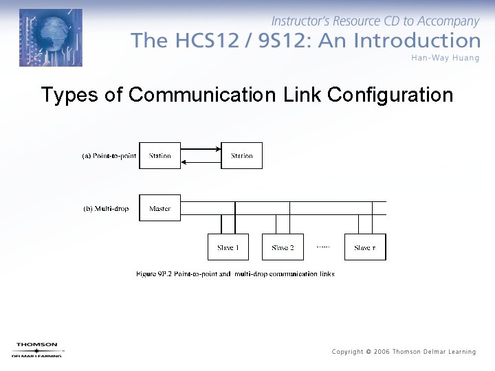
Asynchronous Serial Data Communication • It is often used for data communication between a DTE and a DCE with or without a modem. • DTE stands for data terminal equipment and can be either a computer or a terminal. • DCE stands for data communication equipment. A modem is a DCE. • A basic data communication link is shown. • There are three kinds of data communication links: – Simplex link – Half-duplex link – Full-duplex link

Types of Communication Link Configuration

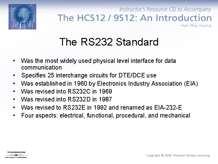
The RS 232 Standard • Was the most widely used physical level interface for data communication • Specifies 25 interchange circuits for DTE/DCE use • Was established in 1960 by Electronics Industry Association (EIA) • Was revised into RS 232 C in 1969 • Was revised into RS 232 D in 1987 • Was revised to RS 232 E in 1992 and renamed as EIA-232 -E • Four aspects: electrical, functional, procedural, and mechanical

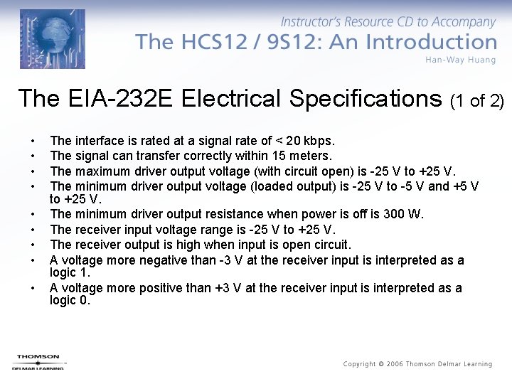
The EIA-232 E Electrical Specifications (1 of 2) • • • The interface is rated at a signal rate of < 20 kbps. The signal can transfer correctly within 15 meters. The maximum driver output voltage (with circuit open) is -25 V to +25 V. The minimum driver output voltage (loaded output) is -25 V to -5 V and +5 V to +25 V. The minimum driver output resistance when power is off is 300 W. The receiver input voltage range is -25 V to +25 V. The receiver output is high when input is open circuit. A voltage more negative than -3 V at the receiver input is interpreted as a logic 1. A voltage more positive than +3 V at the receiver input is interpreted as a logic 0.

The EIA-232 E Electrical Specifications (2 of 2)

EIA-232 -E Mechanical Specification (1 of 2) • Specifies a 25 -pin connector • Specifies exact dimensions of each pin

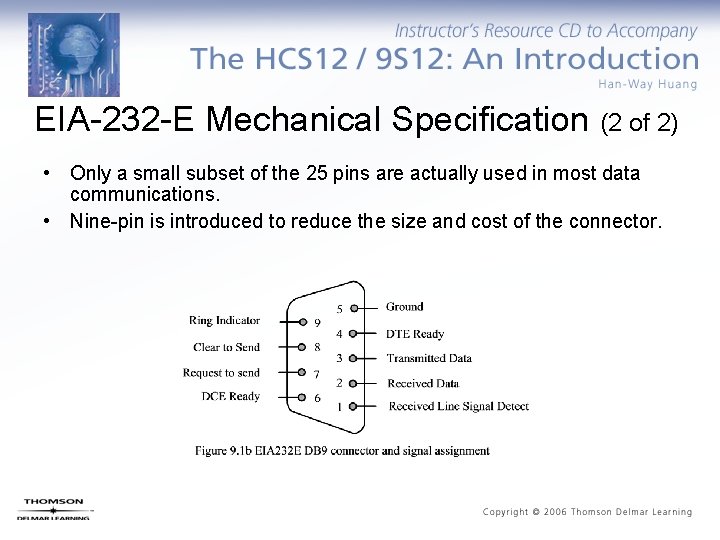
EIA-232 -E Mechanical Specification (2 of 2) • Only a small subset of the 25 pins are actually used in most data communications. • Nine-pin is introduced to reduce the size and cost of the connector.

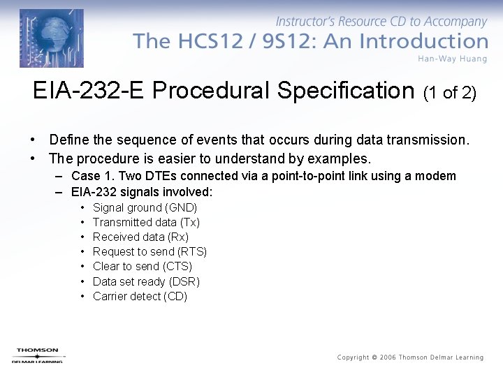
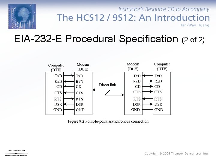
EIA-232 -E Procedural Specification (1 of 2) • Define the sequence of events that occurs during data transmission. • The procedure is easier to understand by examples. – Case 1. Two DTEs connected via a point-to-point link using a modem – EIA-232 signals involved: • • Signal ground (GND) Transmitted data (Tx) Received data (Rx) Request to send (RTS) Clear to send (CTS) Data set ready (DSR) Carrier detect (CD)

EIA-232 -E Procedural Specification (2 of 2)

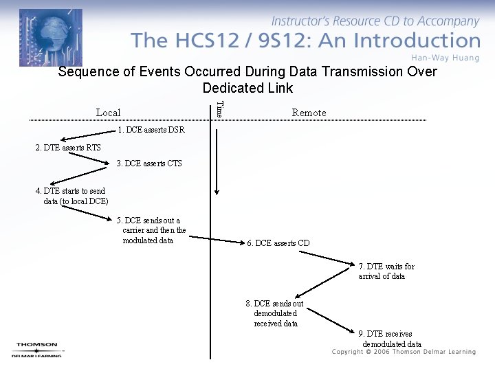
Sequence of Events Occurred During Data Transmission Over Dedicated Link Time Local Remote 1. DCE asserts DSR 2. DTE asserts RTS 3. DCE asserts CTS 4. DTE starts to send data (to local DCE) 5. DCE sends out a carrier and then the modulated data 6. DCE asserts CD 7. DTE waits for arrival of data 8. DCE sends out demodulated received data 9. DTE receives demodulated data

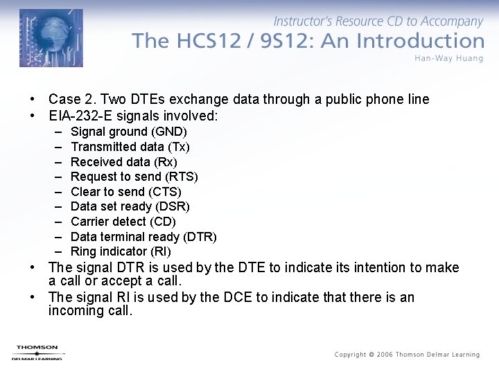
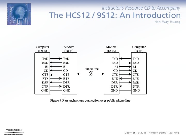
• Case 2. Two DTEs exchange data through a public phone line • EIA-232 -E signals involved: – – – – – Signal ground (GND) Transmitted data (Tx) Received data (Rx) Request to send (RTS) Clear to send (CTS) Data set ready (DSR) Carrier detect (CD) Data terminal ready (DTR) Ring indicator (RI) • The signal DTR is used by the DTE to indicate its intention to make a call or accept a call. • The signal RI is used by the DCE to indicate that there is an incoming call.


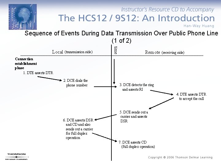
Sequence of Events During Data Transmission Over Public Phone Line (1 of 2) time Local (transmission side) Remote (receiving side) Connection establishment phase 1. DTE asserts DTR 2. DCE dials the phone number 3. DCE detects the ring and asserts RI 4. DTE asserts DTR to accept the call 6. DCE asserts DSR and CD and also sends out a carrier for full duplex operation 5. DCE sends out a carrier and asserts DSR 7. DCE asserts CD (full duplex operation)

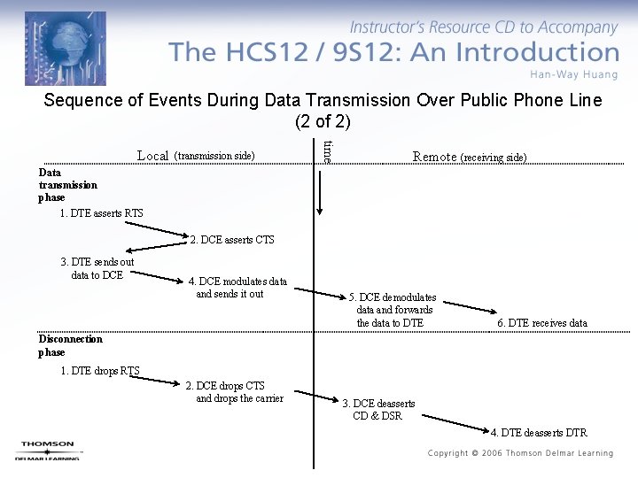
Sequence of Events During Data Transmission Over Public Phone Line (2 of 2) (transmission side) time Local Remote (receiving side) Data transmission phase 1. DTE asserts RTS 2. DCE asserts CTS 3. DTE sends out data to DCE 4. DCE modulates data and sends it out 5. DCE demodulates data and forwards the data to DTE 6. DTE receives data Disconnection phase 1. DTE drops RTS 2. DCE drops CTS and drops the carrier 3. DCE deasserts CD & DSR 4. DTE deasserts DTR

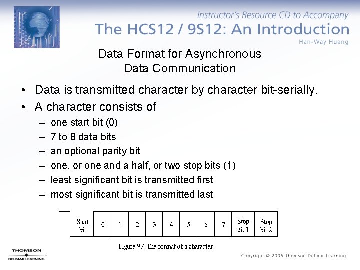
Data Format for Asynchronous Data Communication • Data is transmitted character by character bit-serially. • A character consists of – – – one start bit (0) 7 to 8 data bits an optional parity bit one, or one and a half, or two stop bits (1) least significant bit is transmitted first most significant bit is transmitted last

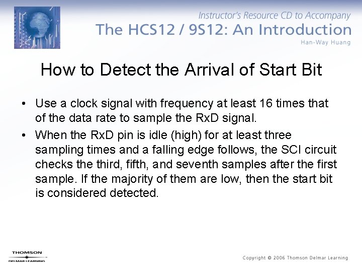
How to Detect the Arrival of Start Bit • Use a clock signal with frequency at least 16 times that of the data rate to sample the Rx. D signal. • When the Rx. D pin is idle (high) for at least three sampling times and a falling edge follows, the SCI circuit checks the third, fifth, and seventh samples after the first sample. If the majority of them are low, then the start bit is considered detected.

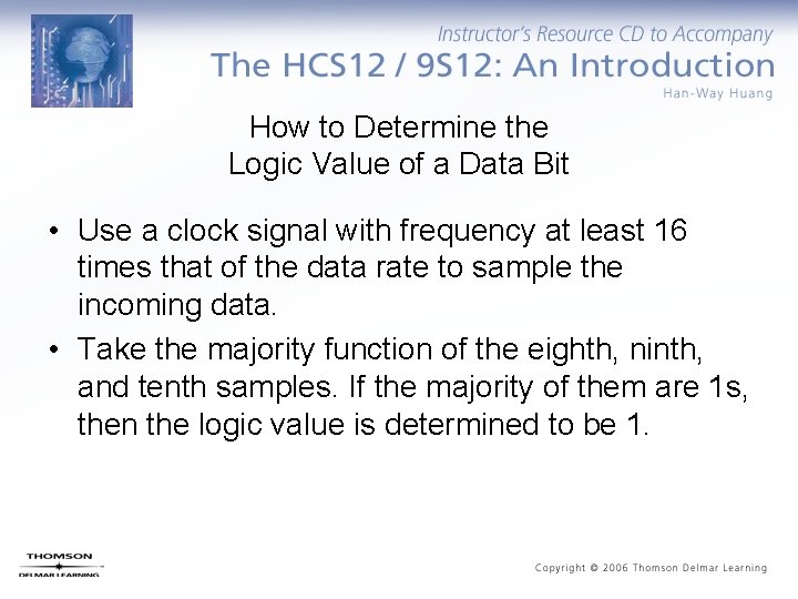
How to Determine the Logic Value of a Data Bit • Use a clock signal with frequency at least 16 times that of the data rate to sample the incoming data. • Take the majority function of the eighth, ninth, and tenth samples. If the majority of them are 1 s, then the logic value is determined to be 1.

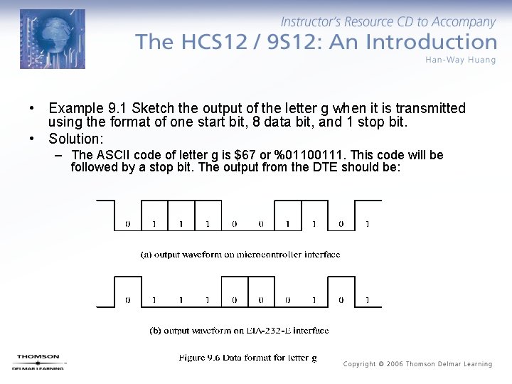
• Example 9. 1 Sketch the output of the letter g when it is transmitted using the format of one start bit, 8 data bit, and 1 stop bit. • Solution: – The ASCII code of letter g is $67 or %01100111. This code will be followed by a stop bit. The output from the DTE should be:

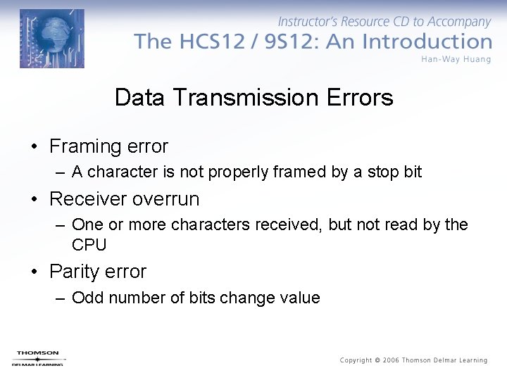
Data Transmission Errors • Framing error – A character is not properly framed by a stop bit • Receiver overrun – One or more characters received, but not read by the CPU • Parity error – Odd number of bits change value

Null Modem Connection

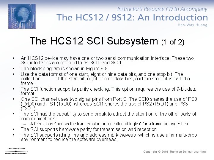
The HCS 12 SCI Subsystem (1 of 2) • • • An HCS 12 device may have one or two serial communication interface. These two SCI interfaces are referred to as SCI 0 and SCI 1. The block diagram is shown in Figure 9. 8. Use the data format of one start, eight or nine data bits, and one stop bit. The collection of the start bit, eight or nine data bits, and the stop bit is called a frame. The SCI function supports parity checking. This option requires the use of 9 -bit data format. One SCI channel uses two signal pins from Port S. The SCI 0 shares the use of PS 0 (Rx. D 0) and PS 1 (Tx. D 0), whereas SCI 1 shares the use of PS 2 (Rx. D 1) and PS 3 (Tx. D 1). The SCI has the capability to send break to attract the attention of the other party of communications. – A break is defined as the transmission or reception of logic 0 for a frame or longer time. • • The SCI supports hardware parity for transmission and reception. The SCI supports idling line and address mark wakeup, which is useful in multi-drop environment to reduce the software overhead.

The HCS 12 SCI Subsystem (2 of 2)

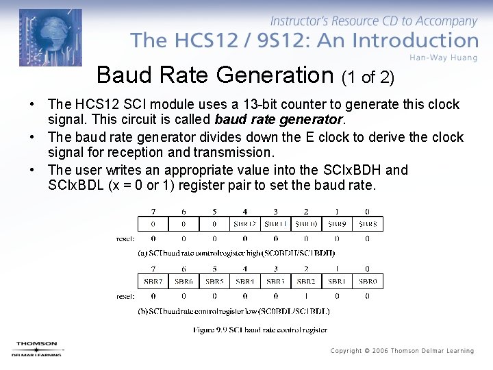
Baud Rate Generation (1 of 2) • The HCS 12 SCI module uses a 13 -bit counter to generate this clock signal. This circuit is called baud rate generator. • The baud rate generator divides down the E clock to derive the clock signal for reception and transmission. • The user writes an appropriate value into the SCIx. BDH and SCIx. BDL (x = 0 or 1) register pair to set the baud rate.

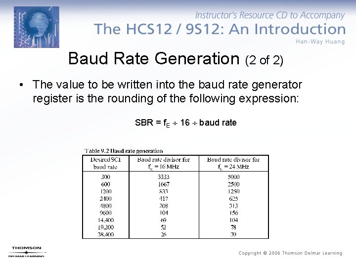
Baud Rate Generation (2 of 2) • The value to be written into the baud rate generator register is the rounding of the following expression: SBR = f. E 16 baud rate

The SCI Control Registers (1 of 2)

The SCI Control Registers (2 of 2)

SCI Status Registers (1 of 2)

SCI Status Registers (2 of 2)

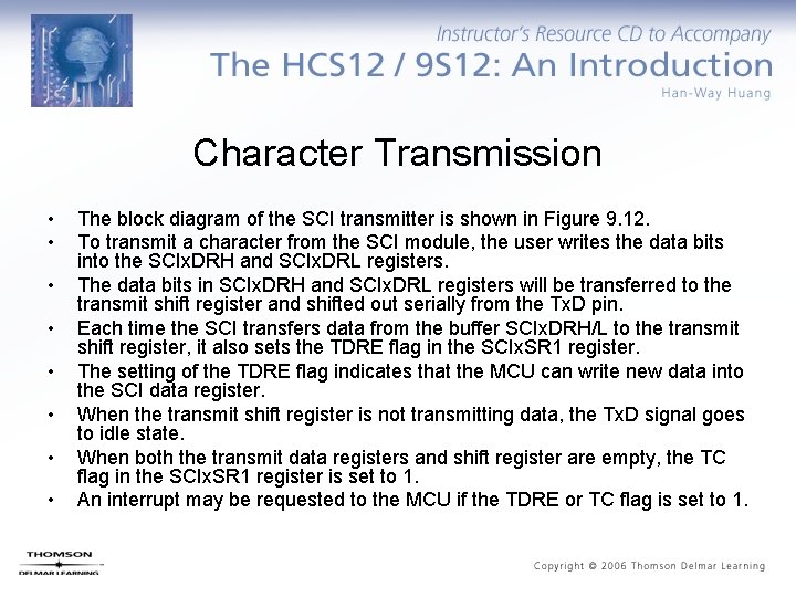
Character Transmission • • The block diagram of the SCI transmitter is shown in Figure 9. 12. To transmit a character from the SCI module, the user writes the data bits into the SCIx. DRH and SCIx. DRL registers. The data bits in SCIx. DRH and SCIx. DRL registers will be transferred to the transmit shift register and shifted out serially from the Tx. D pin. Each time the SCI transfers data from the buffer SCIx. DRH/L to the transmit shift register, it also sets the TDRE flag in the SCIx. SR 1 register. The setting of the TDRE flag indicates that the MCU can write new data into the SCI data register. When the transmit shift register is not transmitting data, the Tx. D signal goes to idle state. When both the transmit data registers and shift register are empty, the TC flag in the SCIx. SR 1 register is set to 1. An interrupt may be requested to the MCU if the TDRE or TC flag is set to 1.


Send Break Characters • A break character is represented by eight or nine logic 0 data bits depending on the character data length. • Whenever one party in the data communications discovers an error, it can send break characters to discontinue the communication and start over again. • To send break characters, the user sets the SBK bit in the SCIx. CR 1 register to 1. • As long as the SBK bit is 1, the transmitter logic continuously sending out the break character.

Idle Characters • An idle character contains all 1 s and has no start, stop, or parity bit. • Depending on the character data length, an idle character can be eight or nine 1 s. • If the TE bit in the SCIx. CR 2 register is cleared during a transmission, the Tx. D signal becomes idle after the completion of the transmission in progress.

Character Reception (1 of 2) • The block diagram of the SCI receiver is shown in Figure 9. 15. • The SCI receiver can handle either 8 - or 9 -bit characters. • When receiving 9 -bit data, the R 8 bit of the SCIx. DRH register holds the ninth bit. • During an SCI reception, the receive shift register shifts in a frame from the Rx. D pin. • After a complete frame is shifted into the receive shift register, the data portion of the frame is transferred to the SCI data register. The receive data register full flag in the SCIx. SR 1 register is set to 1. • An interrupt may be requested to the MCU is it is enabled.

Character Reception (2 of 2)

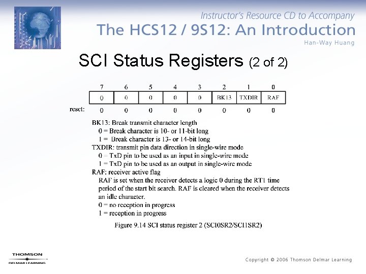
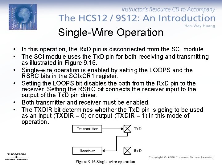
Single-Wire Operation • In this operation, the Rx. D pin is disconnected from the SCI module. • The SCI module uses the Tx. D pin for both receiving and transmitting as illustrated in Figure 9. 16. • Single-wire operation is enabled by setting the LOOPS and the RSRC bits in the SCIx. CR 1 register. • Setting the LOOPS bit disables the path from the Rx. D pin to the receiver. Setting the RSRC bit connects the receiver input to the output of the Tx. D pin driver. • Both transmitter and receiver must be enabled. • The TXDIR bit determines whether the Tx. D pin is going to be used as an input (TXDIR = 0) or output (TXDIR = 1) in this mode of operation.

Flow Control of UART in Asynchronous Mode • • • The SCI module will transmit data as fast as the baud rate allows. In some circumstances, the software may not be able to read data as fast as the data is received. There is a need for the MCU to tell the transmitting device to suspend transmission of data temporarily. Similarly, the HCS 12 may need to be told to suspend transmission temporarily. This is done by flow control. There are two common methods of flow control: XON/XOFF and hardware. XON/XOFF is implemented completely in software, but requires a full-duplex communication. When incoming data needs to be suspended, an XOFF byte is transmitted back to the other device that is transmitting. To start the other device transmitting again, an XON character is transmitted. The XON and XOFF characters have the ASCII code of 0 x 11 and 0 x 13, respectively. Hardware flow control requires the use of extra signals. Generally, an input pin of the transmitter is controlled by the receiver. Before transmitting any character, the transmitter needs to test the flow control input pin.

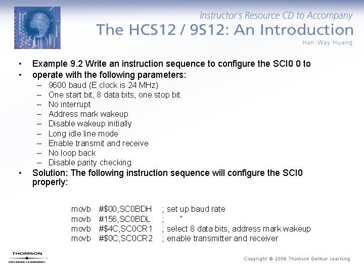
• • Example 9. 2 Write an instruction sequence to configure the SCI 0 0 to operate with the following parameters: – – – – – • 9600 baud (E clock is 24 MHz) One start bit, 8 data bits, one stop bit No interrupt Address mark wakeup Disable wakeup initially Long idle line mode Enable transmit and receive No loop back Disable parity checking Solution: The following instruction sequence will configure the SCI 0 properly: movb #$00, SC 0 BDH #156, SC 0 BDL #$4 C, SC 0 CR 1 #$0 C, SC 0 CR 2 ; set up baud rate ; “ ; select 8 data bits, address mark wakeup ; enable transmitter and receiver

Interfacing SCI with EIA-232 -E • • • The SCI uses 0 V and 5 V to represent 0 and 1. The EIA-232 signal Tx cannot be driven by the SCI Tx. D signal without translation. The EIA-232 signal Rx cannot drive the SCI Rx. D signal without translation. Voltage level translation is required for the SCI signals to drive and be driven by the EIA-232 signals. Examples of EIA-232 driver chips include: – – – • LT 1080/1081 from Linear technology ST 232 from SGS Thompson ICL 232 from Intersil MAX 232 from MAXIM DS 14 C 232 from National Semiconductor These chips are pin-compatible. The DS 14 C 232 from National Semiconductor will be used in the following illustration.


• Interfacing the HCS 12 SCI 0 to the EIA-232 using the DS 14 C 232 chip and implements the NULL modem connection so that this connection can talk to a PC directly.

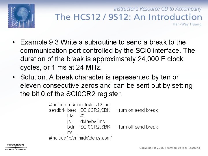
• Example 9. 3 Write a subroutine to send a break to the communication port controlled by the SCI 0 interface. The duration of the break is approximately 24, 000 E clock cycles, or 1 ms at 24 MHz. • Solution: A break character is represented by ten or eleven consecutive zeros and can be sent out by setting the bit 0 of the SCI 0 CR 2 register. #include "c: miniidehcs 12. inc" sendbrk bset SCI 0 CR 2, SBK ; turn on send break ldy #1 jsr delayby 1 ms bclr SCI 0 CR 2, SBK ; turn off send break rts #include “c: miniidedelay. asm”

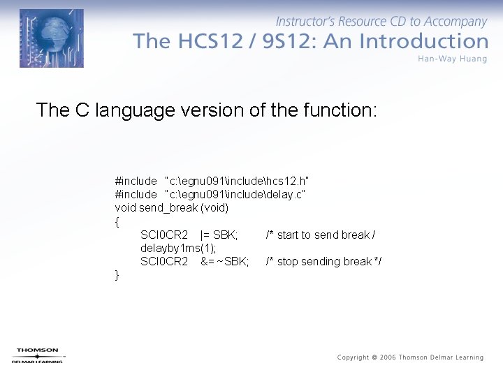
The C language version of the function: #include “c: egnu 091includehcs 12. h” #include “c: egnu 091includedelay. c” void send_break (void) { SCI 0 CR 2 |= SBK; /* start to send break / delayby 1 ms(1); SCI 0 CR 2 &= ~SBK; /* stop sending break */ }

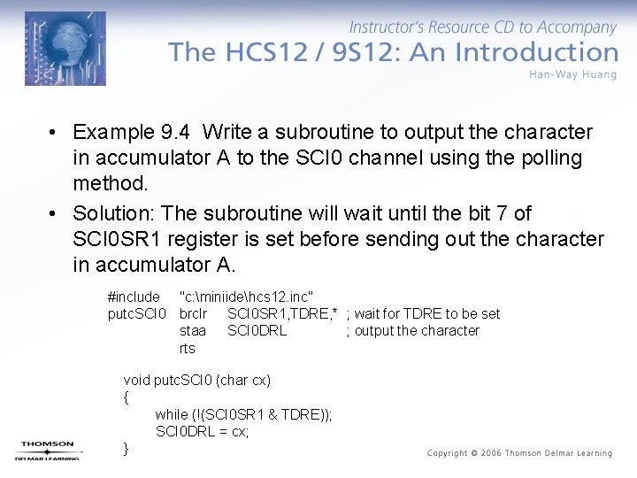
• Example 9. 4 Write a subroutine to output the character in accumulator A to the SCI 0 channel using the polling method. • Solution: The subroutine will wait until the bit 7 of SCI 0 SR 1 register is set before sending out the character in accumulator A. #include "c: miniidehcs 12. inc" putc. SCI 0 brclr SCI 0 SR 1, TDRE, * ; wait for TDRE to be set staa SCI 0 DRL ; output the character rts void putc. SCI 0 (char cx) { while (!(SCI 0 SR 1 & TDRE)); SCI 0 DRL = cx; }

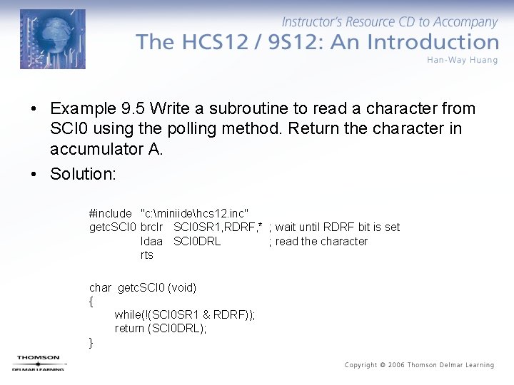
• Example 9. 5 Write a subroutine to read a character from SCI 0 using the polling method. Return the character in accumulator A. • Solution: #include "c: miniidehcs 12. inc" getc. SCI 0 brclr SCI 0 SR 1, RDRF, * ; wait until RDRF bit is set ldaa SCI 0 DRL ; read the character rts char getc. SCI 0 (void) { while(!(SCI 0 SR 1 & RDRF)); return (SCI 0 DRL); }

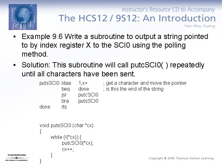
• Example 9. 6 Write a subroutine to output a string pointed to by index register X to the SCI 0 using the polling method. • Solution: This subroutine will call putc. SCI 0( ) repeatedly until all characters have been sent. puts. SCI 0 ldaa beq jsr bra done rts 1, x+ ; get a character and move the pointer done ; is the end of the string putc. SCI 0 puts. SCI 0 void puts. SCI 0 (char *cx) { while (!(*cx)) { putc. SCI 0(*cx); cx++; } }

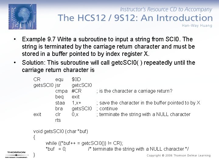
• Example 9. 7 Write a subroutine to input a string from SCI 0. The string is terminated by the carriage return character and must be stored in a buffer pointed to by index register X. • Solution: This subroutine will call getc. SCI 0( ) repeatedly until the carriage return character is CR equ gets. SCI 0 jsr cmpa beq staa bra exit clr rts $0 D getc. SCI 0 #CR exit 1, x+ gets. SCI 0 0, x ; is the character a carriage return? ; save the character in the buffer pointed to by X ; continue ; terminate the string with a NULL character void gets. SCI 0 (char *buf) { while ((*buf++ = getc. SCI 0()) != CR); *buf = 0; /* terminate the string with a NULL character */ }