Microprocessors and Applications SPI Master Synchronous Serial Port


 • จากบลอคไดอะแกรมจะเหนวา § สญญาณนาฬกาของ วธคอ SPI")


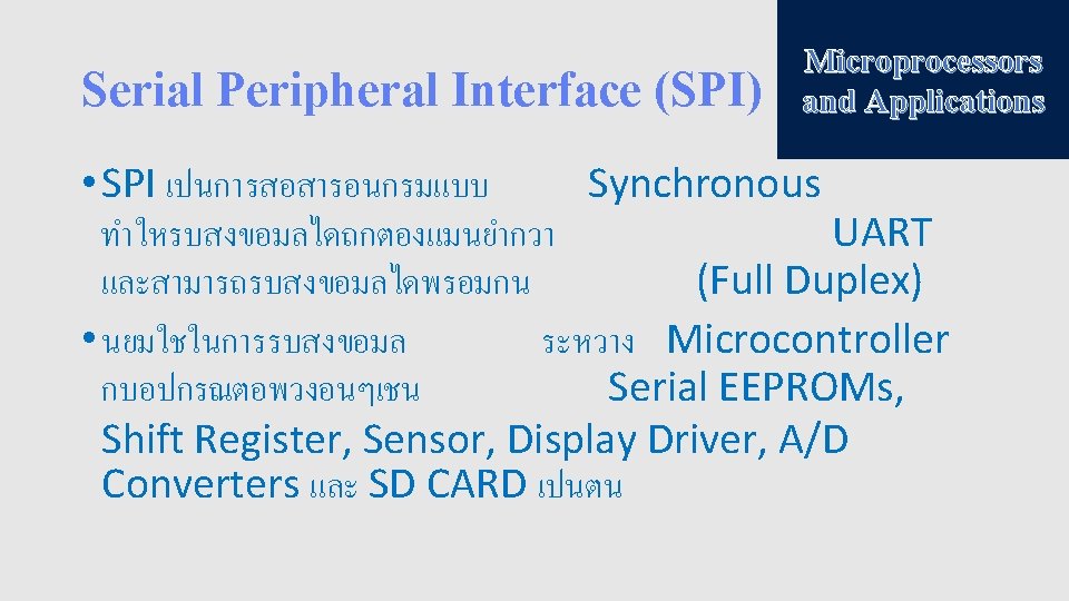
 Microprocessors and Applications")
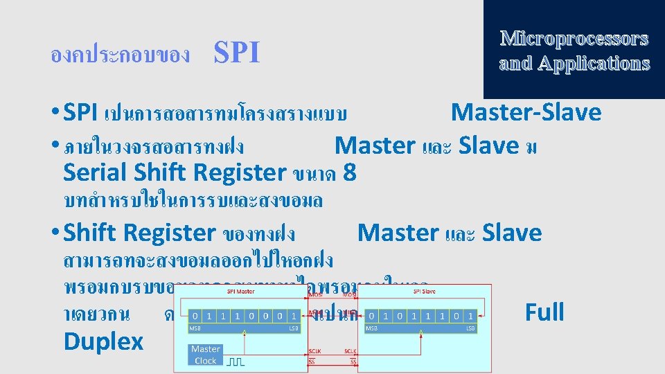
 Microprocessors and Applications")


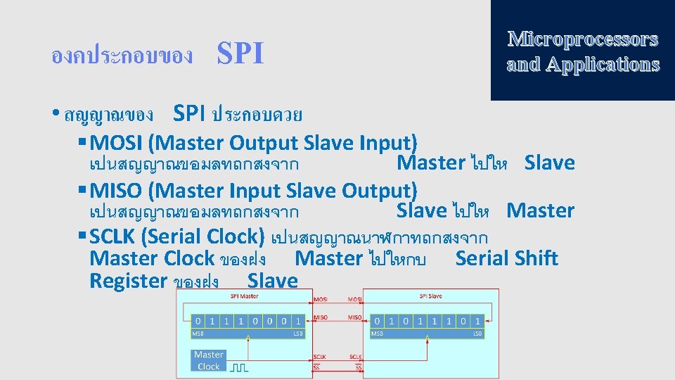
 SPI unsigned char SPI_Read(unsigned char addr)")
 { SPI SSPSTAT = 0 x 40; // Set SMP=0 and")
 { // Button")
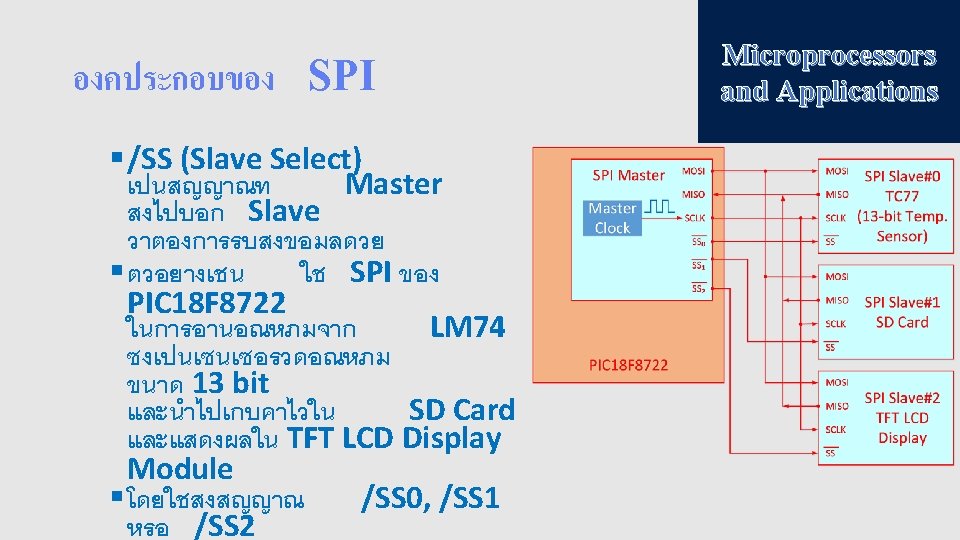
- Slides: 23
Microprocessors and Applications SPI
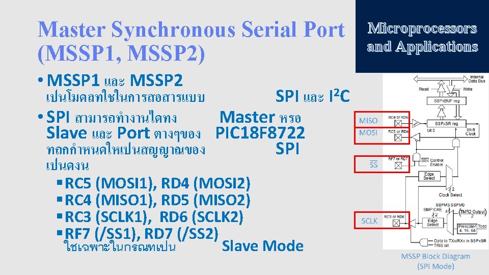
Master Synchronous Serial Port (MSSP 1, MSSP 2) • จากบลอคไดอะแกรมจะเหนวา § สญญาณนาฬกาของ วธคอ SPI สามารถสรางได q. Timer 2 Output/2 (SSPM 3: SSPM 0 = 0011) qวงจร Oscillator ของ PIC 18 F 8722 โดยสามารถเลอกไดวาจะใหมความถเทากบ o Fosc/4 (SSPM 3: SSPM 0 = 0000) o Fosc/16 (SSPM 3: SSPM 0 = 0001) o Fosc/64 (SSPM 3: SSPM 0 = 0010) 2 Microprocessors and Applications
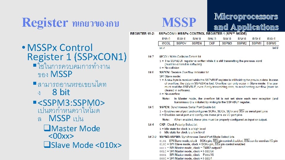
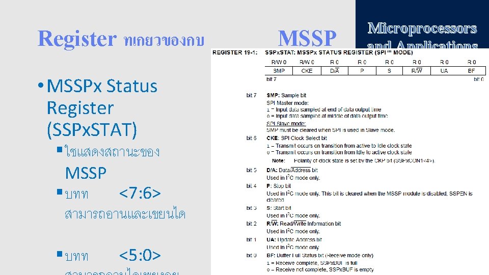
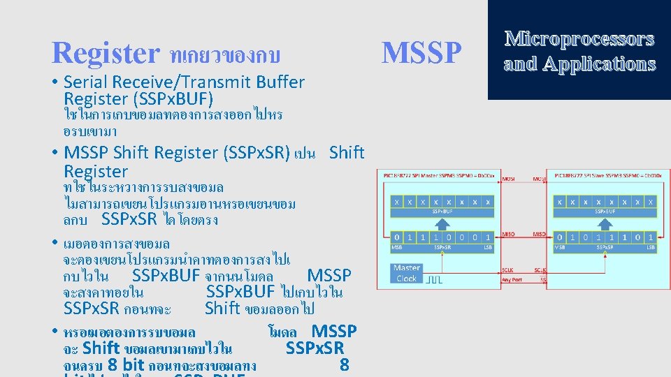
Register ทเกยวของกบ MSSP Microprocessors and Applications
Slave Synchronization Waveform Microprocessors and Applications
SPI Mode Waveform (Slave Mode with CKE = 0) Microprocessors and Applications
SPI Mode Waveform (Slave Mode with CKE = 1) Microprocessors and Applications
16 -Bit I/O Expander with Serial Interface Microprocessors and Applications
Microprocessors and Applications
ตวอยางโปรแกรมสอสาร Microprocessors and Applications SPI #include <p 18 f 8722. h> static rom unsigned char led_patern[32] = #include <delays. h> {0 b 00000001, 0 b 00000011, 0 b 00000110, 0 b 00001100, 0 b 00011001, 0 b 0011, 0 b 0110, 0 b 1100, 0 b 10011000, 0 b 00110000, 0 b 01100000, 0 b 11000000, 0 b 10000000, 0 b 00000000, 0 b 0000, 0 b 10000000, 0 b 11000000, 0 b 01100000, 0 b 00110000, 0 b 10011000, 0 b 1100, 0 b 0110, 0 b 0011, 0 b 00011001, 0 b 00001100, 0 b 00000110, 0 b 00000011, 0 b 00000000, // MCP 23 S 17 SPI Slave Device #define SPI_SLAVE_ID 0 x 40 #define SPI_SLAVE_ADDR 0 x 00 // A 2=0, A 1=0, A 0=0 #define SPI_SLAVE_WRITE 0 x 00 #define SPI_SLAVE_READ 0 x 01 // MCP 23 S 17 Registers Definition for BANK=0 (default) #define IODIRA 0 x 00 #define IODIRB 0 x 01 0 b 0000, 0 b 0000}; // Delay in 1 ms (approximately) for 16 MHz Internal Clock void delay_ms(unsigned int ms) { do { #define IOCONA 0 x 0 A Delay 1 KTCYx(4); #define GPPUA 0 x 0 C #define GPPUB 0 x 0 D #define GPIOA 0 x 12 #define GPIOB 0 x 13 } while(--ms); }
ตวอยางโปรแกรมสอสาร void SPI_Write(unsigned char addr, unsigned char data) SPI unsigned char SPI_Read(unsigned char addr) { { // Activate the SS SPI Select pin PORTCbits. RC 2 = 0; // Start MCP 23 S 17 Op. Code transmission SSPBUF = SPI_SLAVE_ID | ((SPI_SLAVE_ADDR << 1) & 0 x 0 E)| SPI_SLAVE_WRITE; } Microprocessors and Applications SSPBUF = SPI_SLAVE_ID | ((SPI_SLAVE_ADDR << 1) & 0 x 0 E)| SPI_SLAVE_READ; // Wait for Data Transmit/Receipt complete while(!SSPSTATbits. BF); // Start MCP 23 S 17 Address transmission // Start MCP 23 S 17 Register Address transmission SSPBUF = addr; // Wait for Data Transmit/Receipt complete while(!SSPSTATbits. BF); // Send Dummy transmission for reading the data // Start Data transmission SSPBUF = 0 x 00; SSPBUF = data; // Wait for Data Transmit/Receipt complete while(!SSPSTATbits. BF); // CS pin is not active PORTCbits. RC 2 = 1; return(SSPBUF); }
ตวอยางโปรแกรมสอสาร void main(void) { SPI SSPSTAT = 0 x 40; // Set SMP=0 and CKE=1. Notes: The lower 6 bit is read only SSPCON 1 = 0 x 20; // Enable SPI Master with Fosc/4 unsigned char cnt, togbutton, inp; PORTCbits. RC 6 = 1; // Disable Chip Select unsigned int idelay; TRISC = 0 x 00; // Set All on PORTC as Output // Initial the MCP 23 S 17 SPI I/O Expander SPI_Write(IOCONA, 0 x 28); // I/O Control Register: BANK=0, SEQOP=1, HAEN=1 (Enable Addressing) Vss) Microprocessors and Applications SPI_Write(IODIRA, 0 x 00); // GPIOA As Output /* Init the PIC 18 F 14 K 22 ADC Peripheral */ SPI_Write(IODIRB, 0 x. FF); // GPIOB As Input ADCON 0=0 b 00001101; // ADC port channel 3 (AN 3), Enable ADC SPI_Write(GPPUB, 0 x. FF); // Enable Pull-up Resistor on GPIOB ADCON 1=0 b 0000; // Use Internal Voltage Reference (Vdd and SPI_Write(GPIOA, 0 x 00); // Reset Output on GPIOA // Initial Variable Used ADCON 2=0 b 10101011; // Right justify result, 12 TAD, Select the FRC for 16 MHz togbutton=0; // Toggle Button /* Initial the PIC 18 F 14 K 22 SPI Peripheral */ cnt=0; TRISCbits. TRISC 2 = 0; // RC 6/SS - Output (Chip Select) idelay=100; // Default Delay; TRISCbits. TRISC 5= 0; // RC 7/SDO - Output (Serial Data Out) TRISBbits. TRISB 4= 1; // RB 4/SDI - Input (Serial Data In) TRISBbits. TRISB 2= 0; // RB 6/SCK - Output (Clock) for(; ; ) { inp=SPI_Read(GPIOB); // Read from GPIOB
ตวอยางโปรแกรมสอสาร Microprocessors and Applications SPI if (inp == 0 x. FE) { // Button is pressed delay_ms(1); // Write to GPIOA SPI_Write(GPIOA, led_patern[cnt++]); if(cnt >= 32) cnt=0; inp=SPI_Read(GPIOB); // Read from GPIOB, for simple debounce } delay_ms(idelay); // Call Delay function if (inp == 0 x. FE) togbutton^=0 x 01; if (togbutton == 0 x 00) { SPI_Write(GPIOA, 0 x 00); // Write to MCP 23 S 17 GPIOA cnt=0; } } if (togbutton) { ADCON 0 bits. GO=1; while (ADCON 0 bits. GO); // Wait conversion done idelay=ADRESL; // Get the 8 bit LSB result idelay += (ADRESH << 8); // Get the 2 bit MSB result } }