DigitaltoAnalog Converter DAC AnalogtoDigital Converter ADC 1 D
 Analog-to-Digital Converter (ADC) 1")


 3 -bit string DAC: Vref and gnd 8 unit")


 for")


 – Va(C 0))/(C 1")
=INL(C 1)=0 – INL(k) before C 0")


<Va(k-1), non-monotonic at code k")


 = round( (A")


 – The straightforward approach to testing settling")


- Slides: 90
Digital-to-Analog Converter (DAC) Analog-to-Digital Converter (ADC) 1
D n D DAC D There may be a separate –VREF also. Vo Vo V 2
Transfer Curve for Ideal Unipolar 3 -bit DAC VRef FSR VLSB DAC transfer curve has only finite # of discrete points! 3
Ideal DAC 4
Offset binary code for 3 -bit DAC VRef FSR VLSB -VRef VREFP = +VRef , VREFN = –VRef 5
There may be a separate –VREF also. 6
Transfer Curve for Ideal Unipolar 3 -bit ADC VRef ADC transfer curve is a connected curve. 7
Ideal ADC 8
Offset binary code for 3 -bit ADC -VRef 9
Ideal transfer curve of high resolution converters 10
HW: DAC modeling • Every student group will create a Matlab model of a DAC • To be shared with all students • Talk among all, but select your own architecture • For static models, Vo=Vo(Din) • Model consists of a vector of Vo’s, indexed with the DAC input code Din. 11
12
Vo 4 6 3 5 1 t Din 13
HW: DAC modeling • For dynamic models, include only the previous code dependence • For each code transition, the output is not a single value, but a waveform made of a select number of samples • For the first value in Din, just get the static Vo • Beginning from the second values in Din, the waveform depends on both the previous code and the current code 15
HW: DAC modeling • For each of these transitions, we can model it with a 1 st or 2 nd order step response of an RC circuit • The R and C values corresponding to each Din can be computed with the static model • The RC parameterized step responses are used to interpolate between the static Vo to create the dynamic waveform • Details will be discussed for each DAC 16
The Kelvin Divider (String DAC) 3 -bit string DAC: Vref and gnd 8 unit resistors 8 tap voltages 3 digital input 3 to “ 1 of 8” dec analog Vout buffer V 7 V 6 V 5 V 4 V 3 V 2 + – V 1 V 0 • N-bit version consists of 2 N equal resistors in series and 2 N switches • Need N-bit binary to 1 of 2 N decoder 17 • If input code = k, analog output the kth tap voltage.
Model in Matlab • Vref can also be normalized to 1 • Unipolar V range: 0 to 1 – Alternatively can have two resistors of R/2 at Vref and gnd, shit tap voltages by 0. 5 VLSB • Bipolar V range: -1 to 1 • Resistor can also be normalized to have nominal value of 1 – Rk = Rnom*(1+ek) – ek randomly generated – Make sure Rk >= Rmin. 18
• The standard deviation of ek depends on both the process and the area • Explore how this standard deviation is related to the errors in the transfer curve • For a given DAC, once fabricated, – The Rk values are fixed – The tap voltages are fixed – The static transfer curve is fixed an array containing Vk at k-th entry 19
When DAC code goes from k 1 to k 2, DAC output does not go from Vk 1 to Vk 2 instantaneously. A simple crude model involves RC settling. k. R||(2 N-k)R Ron Rink Ronk Vk Cd Vo Co May even ignore Cd for simplicity. 20
A simple linear RC model • From k 1 to k 2: – Use target code k 2 for RC value – Ro ~= k 2*RN // (2^N – k 2)*RN + Ron – Co ~ constant if transmission gates used – Initial value is Vk 1, on Co – Final value is Vk 2, on Co – 1 st order RC settling closed form solution of waveform 21
If trimming points are included: • After fabrication trimming to make the 3 major nodes to be at approximately the correct voltages • Model as a single string but 4 voltage dividers 22
Thermometer current DACs • • • Output node at virtual ground Each resistor contributes either 0 or Vref/R If input digital code = k, k of the 2 N – 1 switches will be turned on I_out =I 1 + I 2 + … +Ik ≈ k*Vref/R Inherently monotonic 23
Use Matched Current Sources • • • Current mirrors to create identical current sources CMOS current sources are compact Cascode current mirrors to increase output impedence I_out =I 1 + I 2 + … +Ik ≈ k*I Inherently monotonic 24
Use Complementary outputs • Each current source and the two switches form a differential pair • Differential pair input Vinh and vinl are just enough to steer all tail current clearly to left or right • All tail currents in current mirror connection • The on side diff pair transistor and tail current transistor in cascode 25 • Can cascode tail current source, to achieve double cascode R_out
Voltage-Mode Binary-Weighted Resistor DAC R 26
HW for everyone • Generalize the previous page to an N-bit structure • Assume all resistors have ideal values as you specify • Let MSB be controlled by b 1, …, and LSB be controlled by b. N • Show that Vout = sum{ bi * Vref/2^i} for i=1 to N 27
Current-Mode Binary-Weighted DACs 28
4 -Bit R-2 R Ladder Network • • One of the most common DAC building-block structures Uses resistors of only two different values with ratio 2: 1 An N-bit DAC requires 2 N resistors, easily trimmable two ways in which the R-2 R ladder network may be used as a DAC 29
Voltage-Mode R-2 R Ladder • "rungs" or arms of the ladder are switched between VREF and ground • Output node has output impedance = R, may need to buffer 30
HW for everyone • Generalize the previous page to an N-bit structure • Let MSB be controlled by b 1, …, and LSB be controlled by b. N • Show that Vout = sum{ bi * Vref/2^i} for i=1 to N 31
Current-Mode R-2 R Ladder Vref/R • Series R can be used to adjust gain of DAC • R_out is code dependent, leading to DAC nonlinearity 32
HW for everyone • Generalize the previous page to an N-bit structure • Take the resistor at Vref to be 0 • Let MSB be controlled by b 1, …, and LSB be controlled by b. N • Show that Iout = Vref/R * sum{ bi /2^i} for i=1 to N 33
Equal Current Sources Switched into an R-2 R Ladder Network R R • • • DAC output impedance is constant and equal to R Used in high speed video DAC Low output impedance may be problem Can add unit cell MSBs to form segmented structure Can replace the gnd node by an identical R-2 R to form differential structure, which has much better linearity 34
Binary-Weighted Current Sources Switched into a Load • Can replace the LSB current source by this binary array 35
Capacitive Unary-Weighted DAC gnd / Vo C …… C C gnd Vref When input code is k, k of the caps are switched to Vref. 36
Capacitive Binary-Weighted DAC gnd / Vo C …… C/2^N gnd Vref The first N caps are controlled by the N bits Last cap is dummy, always connected to gnd 37
Segmented binary Cap DAC gnd / Vo LSB Cap DAC MSB Cap DAC 38
HW for one group • Create an N-bit segmented CDAC model, with in the 12 to 16 range • MSB segment having 6 bits • The LSB segment N-6 bits • Can have total areas for both segments being equal • Compute appropriate C_bridge to make the total effective cap of the LSB seg equal to the unit cap in the MSB array 39
Segmented Voltage-Output DACs MSB LSB • Coarse string has 2 M equal resistors, must be accurate to M+K bit level • Fine stage K-bit DAC must have K-bit accuracy • Fine stage could be string DAC or R-2 R DAC • Use buffers to isolate the two stages, buffers need to be accurate to 40 the M+K bit level
HW for one group • Model an R DAC, with string coarse DAC and R 2 R interpolating fine DAC • MSB string segment has 5 or 6 bits • LSB R 2 R segment has 6 to 10 bits • Include buffer errors: – Offset, at 1 m. V level random – Gain error, at 0. 1% level random 41
Unbuffered String DACs • • Fine string // R 7 R/8 Total resistance = 8 R, current = Vref/8 R Voltage across fine string = Vref/8 R * 7 R/8 = 7 Vref/64 Each resistor in fine string has voltage = Vref/64 42
Segmented Current-Output DACs • • Instead of turning on and off current, use current steering; Current steering is much faster, suited for high speed Use differential pair as steering switch Use just enough diff voltage to steer the current completely 43
HW for one group • Model thermometer plus R 2 R current DAC • Make the MSB to be 5 or 6 bits • Make the LSB to be 6 to 10 bits • That is: 5 + {6, 7, 8}; or 6+{8, 9, 10} • Add the option of a voltage DAC: – I_out ant I_out_bar goes to an I V buffer 44
HW for one group • Model a thermometer plus R 2 R voltage DAC by applying Vref and gnd at Iout and Iout_bar and taking Vout at Vref node • Make the MSB to be 5 or 6 bits • Make the LSB to be 6 to 10 bits • That is: 5 + {6, 7, 8}; or 6+{8, 9, 10} 45
Thermometer + thermometer segmentation Example use 46
HW for one group • Model the multi-segmented current steering DAC as shown on the last page’s example use • Make the output to be differential with I_out ant I_out_bar • Each unit is a PMOS current source with a differential switch • Consider two cases at the output node: – I_out ant I_out_bar goes through RL to gnd – I_out ant I_out_bar goes to an I V buffer 47
DAC standard test Chapter 6 of book • • Offset, gain error INL, DNL AC test Settling 48
Offset and Gain Error
Offset and Gain Error • Both are absolute errors, measured wrt ideal LSB • LSBi = ideal range / 2^N • Offset = (Va(C 0) – Vi(C 0))/LSBi – C 0 could be 0… 0, or first code whose output is not at the lower rail • GE = (Va(C 1) – Va(C 0))/LSBi – (C 1 – C 0) – C 1 could be 1… 1, or last code whose output is not at the upper rail 50
Offset and Gain Error • The previous slide is end-point fit line based offset and gain error • Re-write GE equation: Va(C 1) = Va(C 0) + (C 1 – C 0 + GE)*LSBi • Fit line connect (C 0, Va(C 0)) and (C 1, Va(C 1)) is: Vfit(C) = Va(C 0) + (C 1 – C 0 + GE)*LSBi *(C – C 0)/(C 1 – C 0) = (C – C 0)*LSBi + Va(C 0) + GE*LSBi *(C – C 0)/(C 1 – C 0) ideal offset gain error 51
Offset and Gain Error • Alternative: gain adjusted mean Vos – Adjust Va(C) for gain error: Vadj(C) = Va(C) – GE*(C – C 0)/(C 1 – C 0)*LSBi – Note: Vadj(C 0) = Va(C 0), Vadj(C 1) = Va(C 0) + (C 1 – C 0)*LSBi – Vos, avg=mean{Vadj(C) – (C 1 -C 0)*LSBi}, over C 0 to C 1 52
Offset and Gain Error • Another Alternative: find best fit line through I/O curve Vfit(C) = Vos + Gain*LSBi *(C – Cos)/(code range) • Define a formula to find offset and gain error 53
Linearity errors • Errors that measure the deviation from a “linear” converter • These are all relative errors • Static linearity errors: – Integral non-linearity errors – Measure deviation of the transfer curve from a straight fit line – Differential non-linearity errors – Measure non-uniformity of how the tap voltages are distributed 54
Methods of Measuring INL
Measuring INL/DNL: end point • Actual LSB = (Va(C 1) – Va(C 0))/(C 1 – C 0) = average step size • End point fit line: –Vepfl is Va(C 0) when input is C 0 –Vepfl is Va(C 1) when input is C 1 –Vepfl(k) = Va(C 0) + (k – C 0)*LSB • INL(k) = (Va(k) – Vepfl(k))/LSB • Overall INL = max (abs(INL(k)) • DNL(k) = (Va(k) – Va(k-1))/LSB – 1 = step size error • Overall DNL = max (abs(DNL(k)) 56
Measuring INL/DNL: end point • Note: INL(C 0)=INL(C 1)=0 – INL(k) before C 0 and after C 1 not defined • DNL(k) not defined for C 0, before C 0, and after C 1 • DNL(k) = INL(k) – INL(k-1) • INL(k) = sum DNL(j), j=C 0+1 to k • To make DNL(k) to have the same k range as INL(k), can let DNL(C 0)=0 57
HW • Prove the properties listed on the previous page. • Use least square error sum as criteria, define the fit line for the best straight line method, and the corresponding INL(k) and DNL(k). What happens to the properties listed on the previous page? 58
Measuring INL/DNL: in computer • Suppose tap voltages are in vector V, and the corresponding codes 0. to 1… 1 are sequentially contained in C • Throw away some initial and last points in V and correspondingly in C • Vdiff = diff(V); • LSB = mean(Vdiff); • DNLk = Vdiff/LSB – 1; DNLk=[0; DNLk]; • INLk = cumsum(DNLk); • DNL = max(|DNLk|); INL = max(|INLk|); 59
HW • Show that the last page corresponds to the end point fit line INL(k), DNL(k) • Show that the following modification produces the LS best fit line INL(k). – A = ones(size(INLk)); – A = [A cumsum(A)]; – X = AINLk; – INLk 1 = INLk – A*X; • How do you obtain best fit line DNLk? 60
Non-monotonic DAC If Va(k)<Va(k-1), non-monotonic at code k
HW • Show that a converter is non-monotonic at code k if and only if DNL(k) < – 1. 62
• Example: • A 4 -bit two’s complement DAC produces the following set of voltage levels, starting from code – 8 and progressing through code +7: -780 m. V, -705 m. V, -530 m. V, -455 m. V, -400 m. V, -325 m. V, -150 m. V, -75 m. V, 120 m. V, 195 m. V, 370 m. V, 445 m. V, 500 m. V, 575 m. V, 750 m. V, 825 m. V.
• The first derivative values are: 75 m. V, 175 m. V, 55 m. V, 75 m. V, 175 m. V, 195 m. V, 75 m. V, 175 m. V, 55 m. V, 75 m. V, 175 m. V, 75 m. V. • The average value of these gives an end-point LSB of 107 m. V. The LS best-fit line calculation gives LSB=109. 35 m. V. Dividing by the LS LSB size yields the normalized derivative curve (in LSBs): 0. 686, 1. 6, 0. 686, 0. 503, 0. 686, 1. 6, 0. 686, 1. 783, 0. 686, 1. 6, 0. 686, 0. 503, 0. 686, 1. 6, 0. 686. • Subtracting one from each of these values gives us the LS best line DNL curve for this DAC: -0. 314, 0. 6, -0. 314, 0. 497, -0. 314, 0. 6, -0. 314, 0. 783, -0. 314, 0. 6, -0. 314, 0. 497, -0. 314, 0. 6, -0. 314.
shows the DNL curve for this DAC. The maximum DNL value is +0. 783 LSB, while the minimum DNL value is – 0. 314. The minimum value is greater than – ½ LSB, but the maximum DNL value is greater than ½ LSB. Therefore, this DAC fails the DNL specification of +/- ½ LSB.
• Using an endpoint calculation method, the INL curve for the 4 -bit DAC of the previous examples is calculated by subtracting a straight line between the – FS voltage and the +FS voltage from the DAC output curve. The difference at each point in the DAC curve is divided by the average LSB size, which in this case is calculated using an endpoint method. As in the endpoint DNL example, the average LSB size is equal to 107 m. V. • The results of the INL calculations are listed below. Again, these values are expressed in LSBs. 0, -0. 299, 0. 336, 0. 037, -0. 449, -0. 748, -0. 112, -0. 411, 0. 112, 0. 748, 0. 449, -0. 37, -0. 336, 0. 299, 0
The figure shows the endpoint INL curve. The maximum INL value is +0. 748 LSB, and the minimum INL value is – 0. 748. This DAC does not pass an INL specification of +/- ½ LSB
• Best Fit Solution – Using a best-fit calculation method, the INL curve for the 4 bit DAC of the previous examples is calculated by subtracting the best-fit line from the DAC output curve. – Each point in the difference curve is divided by the average LSB size, which in this case is calculated using the best-fit line method. As in the best-fit DNL example, the average LSB size is equal to 109. 35 m. V. The results of the INL calculations are listed below, expressed in LSBs. 0. 161, -0. 153, 0. 448, 0. 133, -0. 364, -0. 678, -0. 077, -0. 392, 0. 077, 0. 678, 0. 364, -0. 133, -0. 448, 0. 153, -0. 161 – The best-fit INL curve is shown for comparison with the endpoint INL curve. The maximum value is +0. 678 and the minimum value is – 0. 678.
– The best-fit INL results are better than the endpoint INL values, but still do not pass a +/- ½ LSB test limit. The two INL curves are somewhat similar in shape, but the individual INL values are quite different. – The choice of calculation technique is much more important for INL curves than for DNL curves. – A best-fit curve will usually give better INL results than an endpoint INL calculation
HW • In general, how does the end point INL compare to the LS best line INL? What’s the relationship among them? Can you quickly provide a reasonable guess? Can you quantitatively show or prove your guess? 70
Partial Transfer Curves – A customer or systems engineer may request that a portion of the transfer curve meet certain detailed specifications.
Major Carrier Testing • For binary weighted DACs, ideally if the weight of each bit is known, the whole transfer curve can be computed – For DAC input code, D 0, D 1, . . . Dn. The DAC’s output value is = D 0*W 0+D 1*W 1+. . . +Dn*Wn + DC Base – where: DAC code bits D 0 -Dn take on the value of 1 or 0; W 1 = 2*W 0; W 2 = 2*W 1 … Wn = 2*Wn-1 – DC Base is the DAC output value with a -FS input code
Major Carrier Testing – Measure the DC Base, with minus full scale code – Measure step size at major carrier transitions » V 0 = W 0 » V 1 = W 1 – W 0 » V 2 = W 2 – (W 1+W 0) » V 3 = W 3 – (W 2+W 1+W 0) » . . . » Vn = Wn – (Wn-1+Wn-2+Wn-3. . . W 0) – Solve these equations for the weights
Other Selected-Code Techniques – Besides the major carrier method, other selectedcodes techniques have been developed to reduce the test time associated with all-codes testing. – The simplest of these is the segmented method. This method only works for certain types of DAC and ADC architectures. – Alternatively, “trouble codes” can be identified during characterization. These codes together with certain segments are to be tested in production.
DAC AC test • DAC input: digital sine wave – D(k) = round( (A sin(2 pi J k / M) + 1)/2 * 2^N) – where A is amp, Vref or slightly less – M is the number of DAC output samples to generate – J is the number of sine periods in M points – k is time index ranging 0, 1, 2, to M-1 • DAC output: treat as analog – Use an “ideal” ADC to capture DAC output – Or an ADC with >10 X speed, and >3 extra bits 75
• If ADC is sampling at integer H times DAC clock rate – Samples per DAC clock period is H – Total ADC samples to capture is H*M – Captured data will be coherent • If H is not an integer – You still have H*M points in captured data – But coherent sampling may be lost – Non-coherent sampling FFT may be needed 76
HW • In your DAC model, make sure output switches and capacitors are included. • For simplicity, only model first order RC effects • Assume ADC with infinite resolution and a sampling rate that is an integer times the DAC rate • Select M to be an power of 2, and select J to be odd and J/M in the range of 5 -10%. • Plot the ADC output spectrum. 77
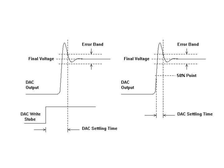
DAC transient test Conversion Time (Settling Time) – The straightforward approach to testing settling time is to digitize the DAC’s output as it transitions from one code to another and then use the known time period between digitizer samples to calculate the settling time. – We measure the final settled voltage, calculate the settled voltage limits (i. e. +/- 1/2 LSB) and then calculate the time between the digital signal transition that initiates a DAC code change and the point at which the DAC first stays within the error band limits
Overshoot, Undershoot • Overshoot and undershoot can also be calculated from the samples collected during the DAC settling time test. These are defined as a percentage of the voltage swing or as an absolute voltage. Below is a DAC output with 50% overshoot and 10% undershoot on a –FS to +FS transition
Rise/Fall Time • Rise and fall time can also be measured from the digitized waveform collected during a settling time test. Rise and fall times are typically defined as the time between two markers, one of which is 10% of the way between the initial value and the final value and the other of which is 90% of the way between these values.
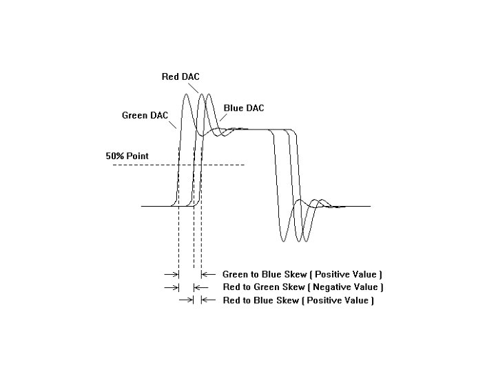
DAC to DAC Skew • Some types of DACs are designed for use in matched groups. – For example, a color palette RAM DAC is a device that is used to produce colors on video monitors. A RAM DAC uses a random access memory (RAM) lookup table to turn a single color value into a set of three DAC output values, representing the red, green, and blue intensity of each pixel. These DAC outputs must change almost simultaneously to produce a clean change from one pixel color to the next. • The degree of mismatch between the three DAC outputs is called DAC-to-DAC skew. It is measured by digitizing each DAC output and comparing the timing of the 50% point of each output to the 50% point of the other outputs. There are three skew values (R-G, G-B, and B-R) as illustrated in the next slide.
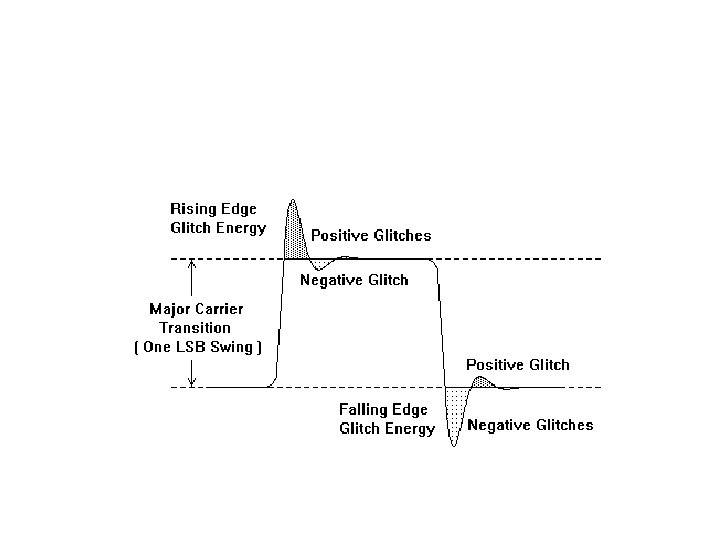
Glitch Energy • Glitch energy is another specification common to high frequency DACs, especially video DACs. It is defined as the total area of the glitches in a DAC’s output as it transitions across the largest major transition (i. e. 01111111 to 10000000 in an 8 -bit DAC) and back again. • The parameter is expressed in picosecond-volts (ps. V). • One area of ambiguity in this specification: is area under the negative-going spike considered negative area, to be subtracted from the area under the positive spike, or is it positive area to be added?
HW • Suppose a DAC is tested and the vectors of input C and output V are available. Vrefb and Vreft are also given for the bottom and top of the reference range. Write a Matlab function to generate the offset, gain error, INLk/DNLk, and INL/DNL, and plot INLk~k, DNLk~k plots. • Suppose the waveform of the DAC output transient (as on the previous page) for two conversions is captured and recorded in V and t vectors. Write a Matlab function to compute the settling time, rise time, overshoot, and glitch energy. 86
Food for thought • Typically in a given technology, available DAC performance is better than available ADC performance (could be quite bit better). • How do you use an ADC to capture the DAC transient waveform? 87
Possibilities • Pedestal DACs • Under-sampling 88
HW Vref=1 V, P=1 m. W, T=27 C, BW=1 MHz. 1. Determine R values. 2. Determine s for 18 bit matching. 3. Generate a 18 bit DAC and fix it. 4. Add a noise V-source for each R. 5. Use a 20 bit linear ADC to measure Vout. ADC has input additive noise s=1 LSB. 6. Sequentially sweep DAC input code from 0 to 2^18 – 1. 7. For each code, take H samples of Vout. Start with H=10, for example. 8. Create a big matrix, with the following columns 1) 2) 3) 4) 5) 6) Sample index DAC input code Ideal DAC output Expected DAC output (output if noise-free and infinite resolution ADC) Actual measured DAC output (20 bit ADC output code in the presence of noise, interpreted in V) TUE (total unadjusted error, = 5) – 3) ) in ideal LSB’s 9. Plot 3)~6) vs 1), or vs 2). zoom in to see details. 10. Use 5) to compute end-point fit line, and LS best fit line. Note: line is Vout vs Din 11. Compute INL and DNL. (both epfl and LSbfl) 12. Compute gain error. (either epfl or LSbfl) 13. Compute Vos: from code C 0, or from gain adjusted average error 89 14. Repeat for 10 H, and/or 10 P, 0. 1 P, and/or 10 BW, 0. 1 BW; and conclude
HW • Show that, regardless how a net work of resistor are connected, the total noise contribution from all resistor to the output node is equal to the noise of an equivalent resistor looking into the output node. • Show that, if we replace all resistors by their nominal values, the noise rms will only change by a negligible amount. • With the above two, a single voltage noise source with psd = 4 k. TR in series with Vout is sufficient. 90