Chapter 8 SPI Protocol and DAC Interfacing 1
![GPIOx_MODER Bits 2 y: 2 y+1 MODERy[1: 0]: Port x configuration bits (y = GPIOx_MODER Bits 2 y: 2 y+1 MODERy[1: 0]: Port x configuration bits (y =](https://slidetodoc.com/presentation_image_h/1112dc02f099fc047f0769099cd878e9/image-21.jpg)
- Slides: 29

Chapter 8 SPI Protocol and DAC Interfacing 1

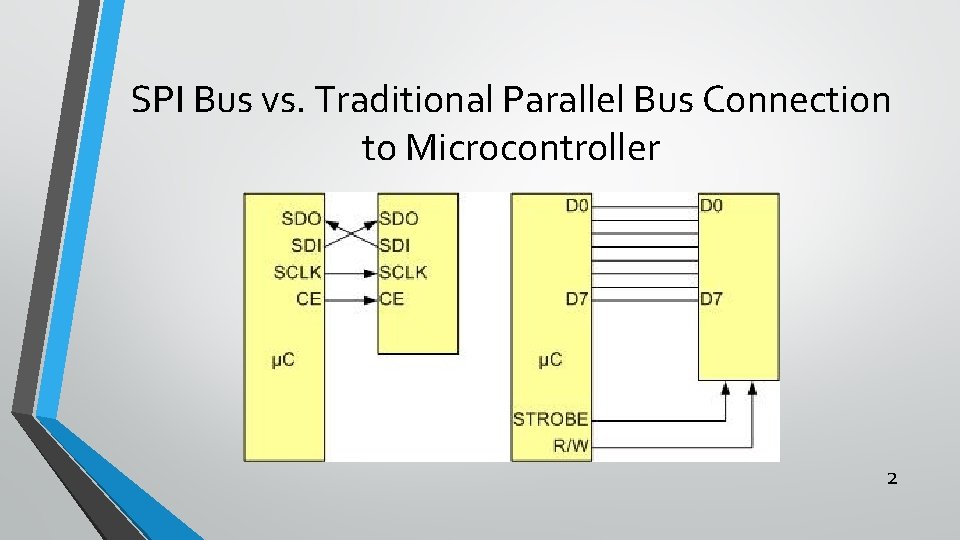
SPI Bus vs. Traditional Parallel Bus Connection to Microcontroller 2

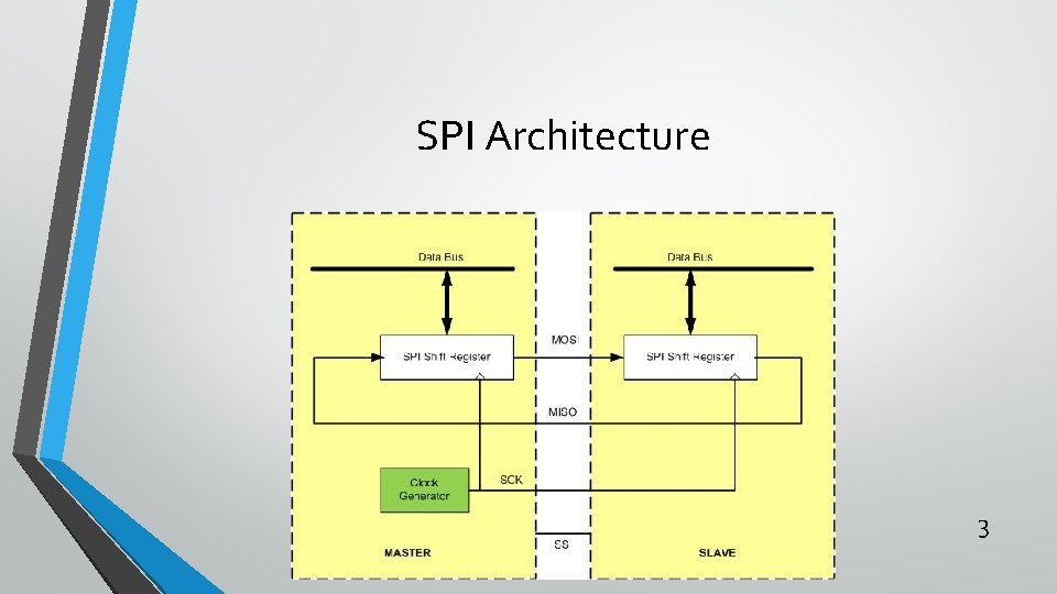
SPI Architecture 3

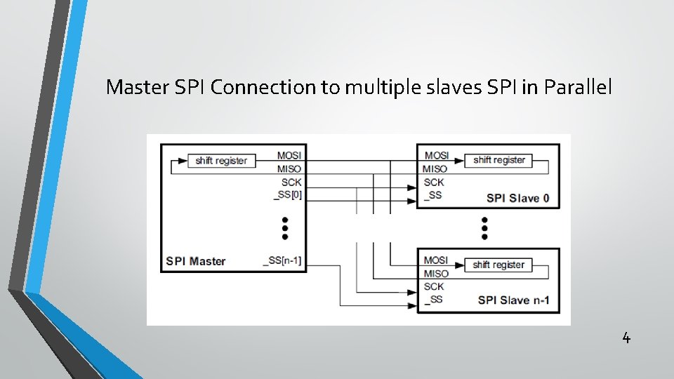
Master SPI Connection to multiple slaves SPI in Parallel 4

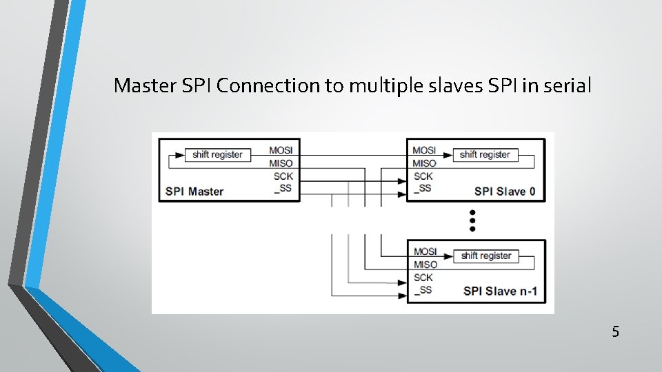
Master SPI Connection to multiple slaves SPI in serial 5

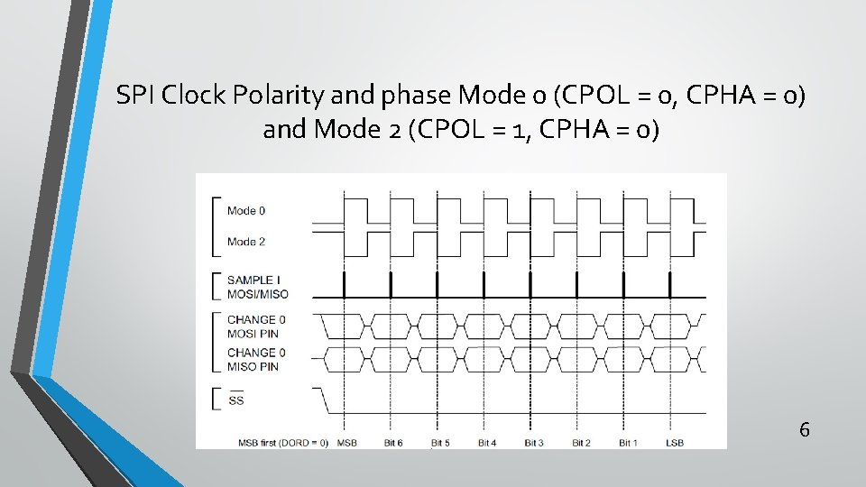
SPI Clock Polarity and phase Mode 0 (CPOL = 0, CPHA = 0) and Mode 2 (CPOL = 1, CPHA = 0) 6

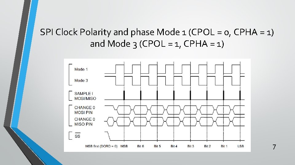
SPI Clock Polarity and phase Mode 1 (CPOL = 0, CPHA = 1) and Mode 3 (CPOL = 1, CPHA = 1) 7

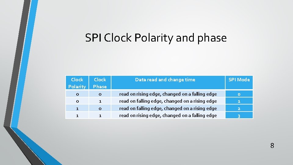
SPI Clock Polarity and phase Clock Polarity 0 0 1 1 Clock Phase 0 1 Data read and change time read on rising edge, changed on a falling edge read on falling edge, changed on a rising edge read on rising edge, changed on a falling edge SPI Mode 0 1 2 3 8

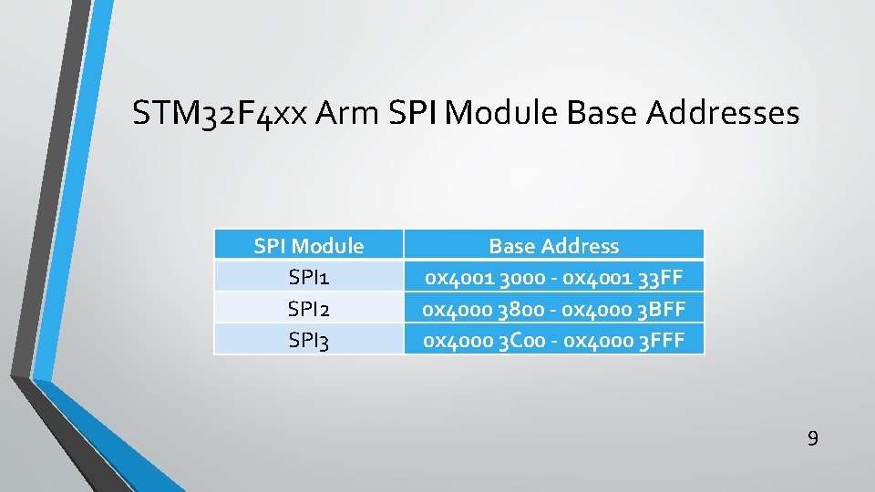
STM 32 F 4 xx Arm SPI Module Base Addresses SPI Module SPI 1 SPI 2 SPI 3 Base Address 0 x 4001 3000 - 0 x 4001 33 FF 0 x 4000 3800 - 0 x 4000 3 BFF 0 x 4000 3 C 00 - 0 x 4000 3 FFF 9

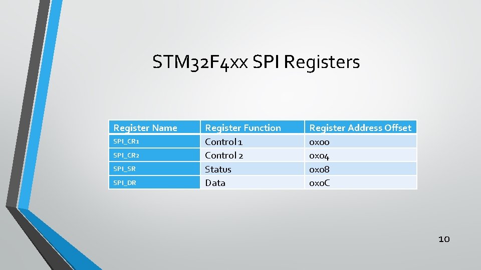
STM 32 F 4 xx SPI Registers Register Name SPI_CR 1 SPI_CR 2 SPI_SR SPI_DR Register Function Control 1 Control 2 Status Data Register Address Offset 0 x 00 0 x 04 0 x 08 0 x 0 C 10

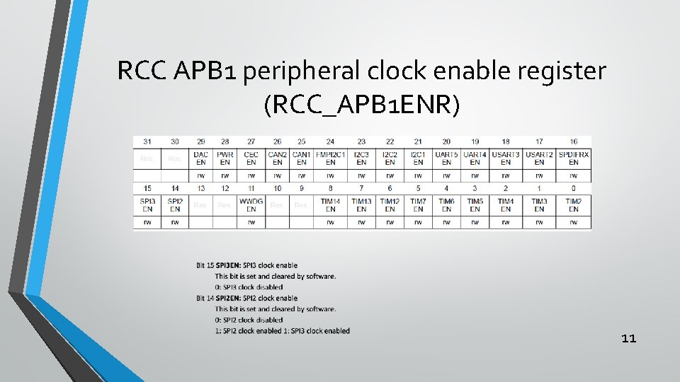
RCC APB 1 peripheral clock enable register (RCC_APB 1 ENR) 11

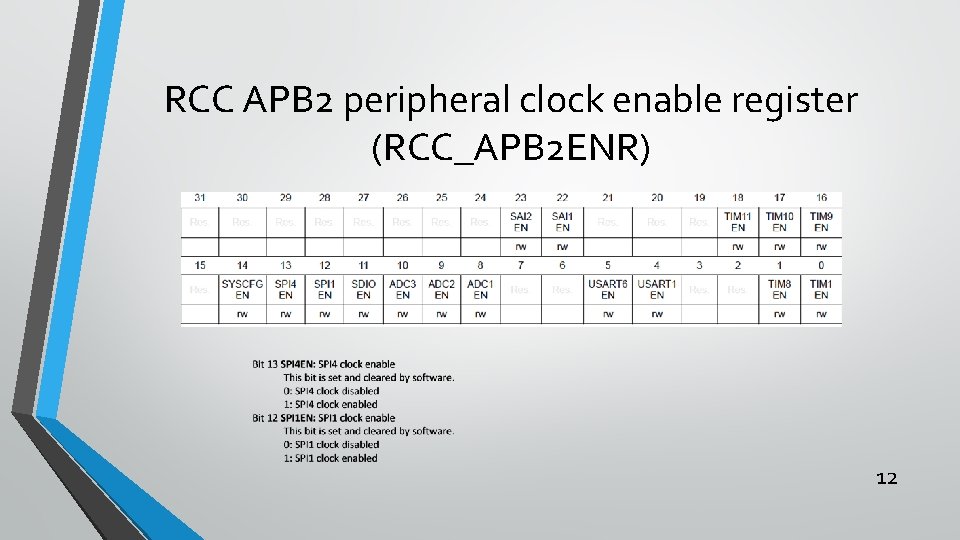
RCC APB 2 peripheral clock enable register (RCC_APB 2 ENR) 12

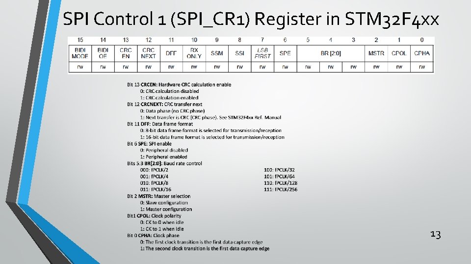
SPI Control 1 (SPI_CR 1) Register in STM 32 F 4 xx 13

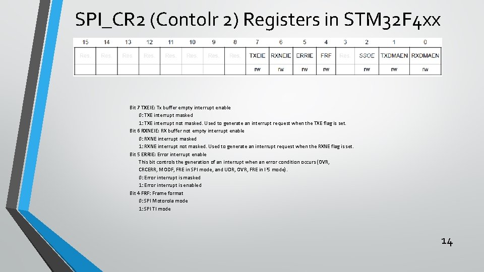
SPI_CR 2 (Contolr 2) Registers in STM 32 F 4 xx Bit 7 TXEIE: Tx buffer empty interrupt enable 0: TXE interrupt masked 1: TXE interrupt not masked. Used to generate an interrupt request when the TXE flag is set. Bit 6 RXNEIE: RX buffer not empty interrupt enable 0: RXNE interrupt masked 1: RXNE interrupt not masked. Used to generate an interrupt request when the RXNE flag is set. Bit 5 ERRIE: Error interrupt enable This bit controls the generation of an interrupt when an error condition occurs (OVR, CRCERR, MODF, FRE in SPI mode, and UDR, OVR, FRE in I 2 S mode). 0: Error interrupt is masked 1: Error interrupt is enabled Bit 4 FRF: Frame format 0: SPI Motorola mode 1: SPI TI mode 14

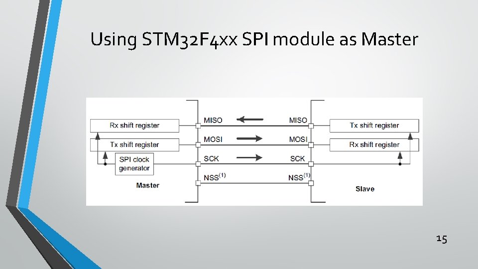
Using STM 32 F 4 xx SPI module as Master 15

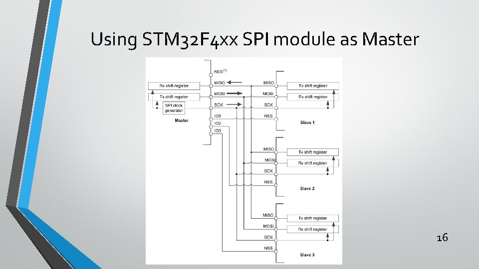
Using STM 32 F 4 xx SPI module as Master 16

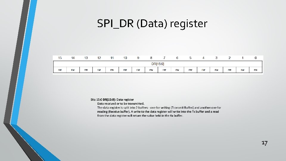
SPI_DR (Data) register 17

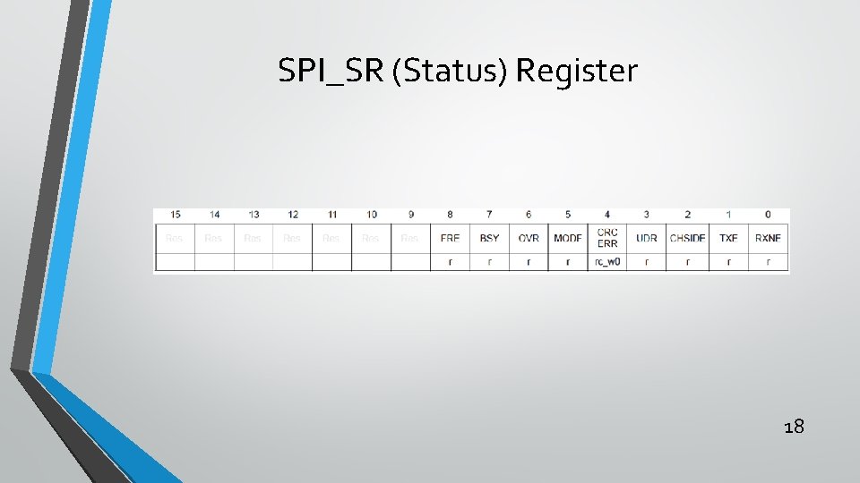
SPI_SR (Status) Register 18

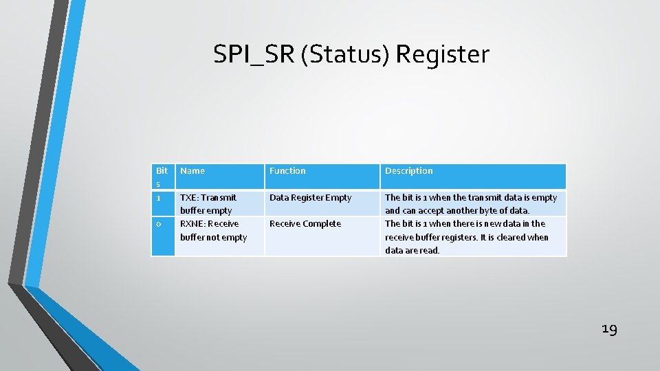
SPI_SR (Status) Register Bit s 1 0 Name Function Description TXE: Transmit buffer empty RXNE: Receive buffer not empty Data Register Empty The bit is 1 when the transmit data is empty and can accept another byte of data. The bit is 1 when there is new data in the receive buffer registers. It is cleared when data are read. Receive Complete 19

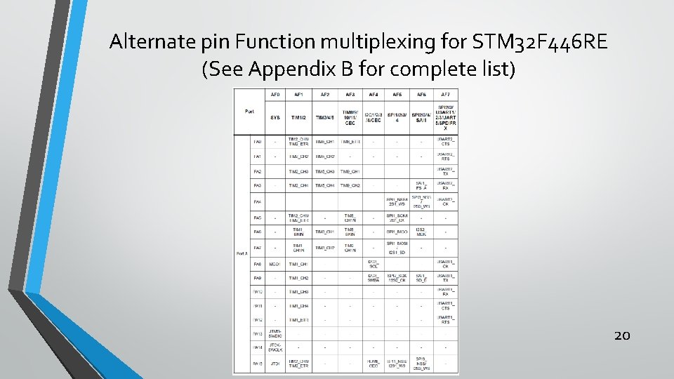
Alternate pin Function multiplexing for STM 32 F 446 RE (See Appendix B for complete list) 20
![GPIOxMODER Bits 2 y 2 y1 MODERy1 0 Port x configuration bits y GPIOx_MODER Bits 2 y: 2 y+1 MODERy[1: 0]: Port x configuration bits (y =](https://slidetodoc.com/presentation_image_h/1112dc02f099fc047f0769099cd878e9/image-21.jpg)
GPIOx_MODER Bits 2 y: 2 y+1 MODERy[1: 0]: Port x configuration bits (y = 0. . 15) These bits are written by software to configure the I/O direction mode. 00: Input (reset state) 01: General purpose output mode 10: Alternate function mode 11: Analog mode 21

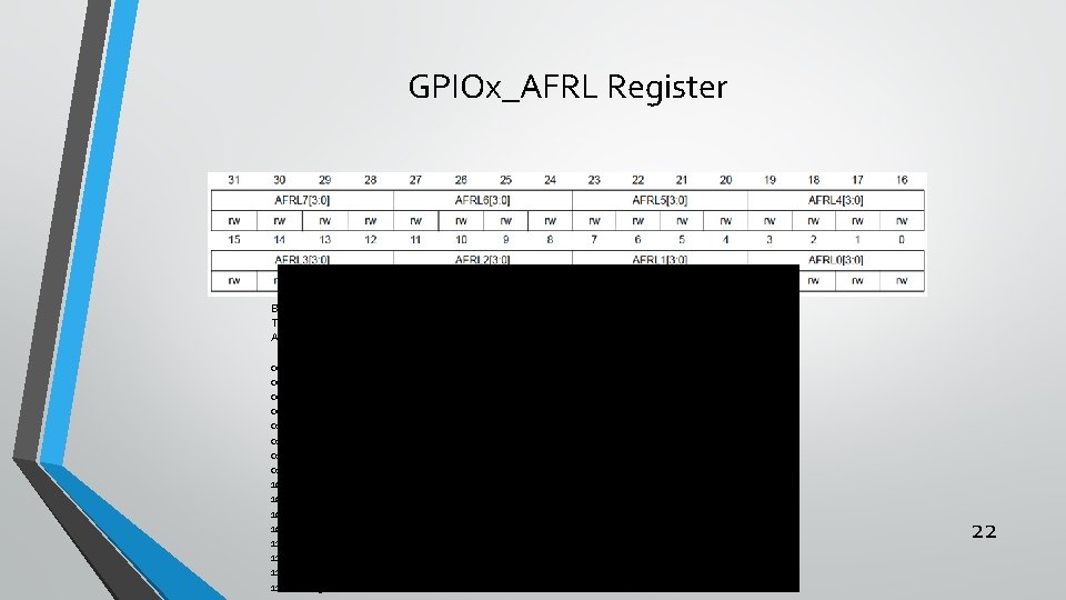
GPIOx_AFRL Register Bits 31: 0 AFRLy: Alternate function selection for port x bit y (y = 0. . 7) These bits are written by software to configure alternate function I/Os AFRLy selection: 0000: AF 0 0001: AF 1 0010: AF 2 0011: AF 3 0100: AF 4 0101: AF 5 0110: AF 6 0111: AF 7 1000: AF 8 1001: AF 9 1010: AF 10 1011: AF 11 1100: AF 12 1101: AF 13 1110: AF 14 1111: AF 15 22

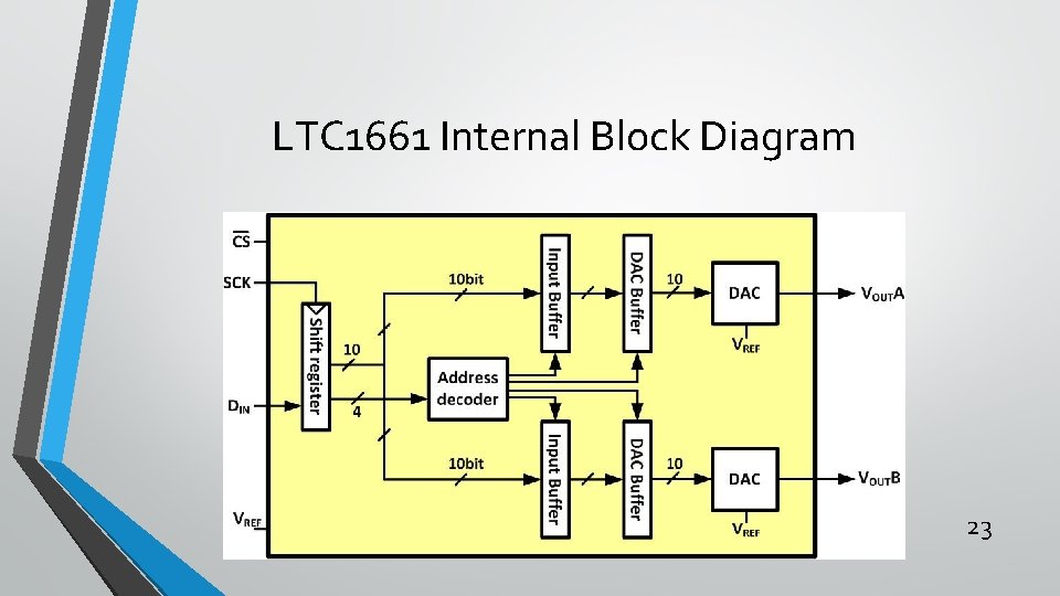
LTC 1661 Internal Block Diagram 23

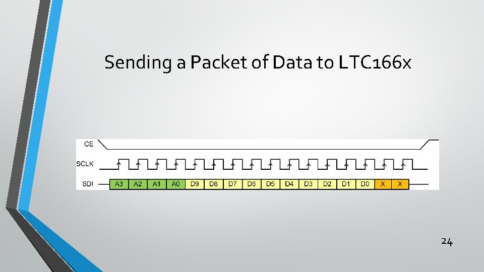
Sending a Packet of Data to LTC 166 x 24

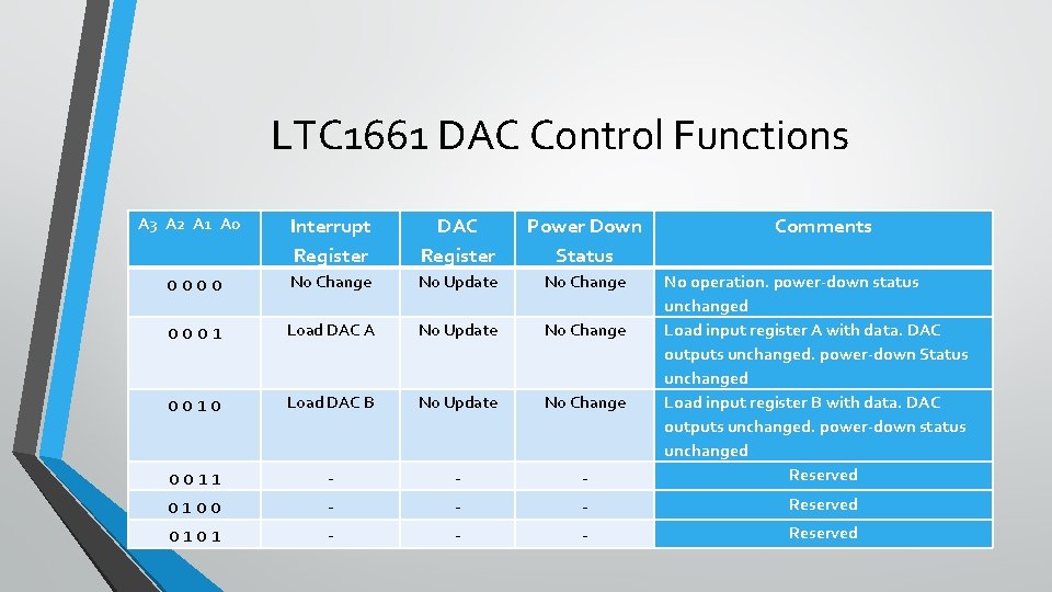
LTC 1661 DAC Control Functions A 3 A 2 A 1 A 0 Interrupt Register DAC Register Power Down Status 0000 No Change No Update No Change 0001 Load DAC A No Update No Change 0010 Load DAC B No Update No Change 0011 0100 0101 - - - Comments No operation. power-down status unchanged Load input register A with data. DAC outputs unchanged. power-down Status unchanged Load input register B with data. DAC outputs unchanged. power-down status unchanged Reserved 25

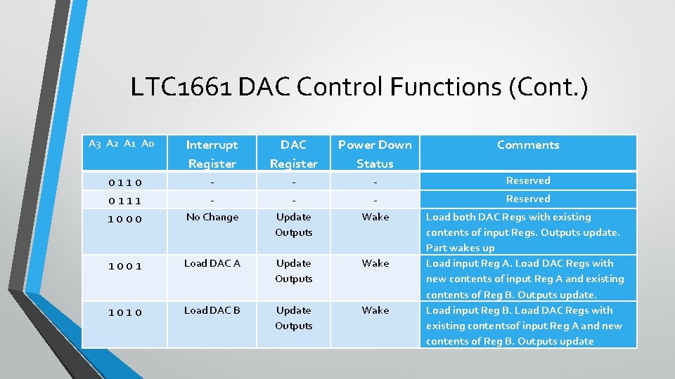
LTC 1661 DAC Control Functions (Cont. ) A 3 A 2 A 1 A 0 Interrupt Register - DAC Register - Power Down Status - Comments No Change Update Outputs Wake 1001 Load DAC A Update Outputs Wake 1010 Load DAC B Update Outputs Wake Load both DAC Regs with existing contents of input Regs. Outputs update. Part wakes up Load input Reg A. Load DAC Regs with new contents of input Reg A and existing contents of Reg B. Outputs update. Load input Reg B. Load DAC Regs with existing contentsof input Reg A and new 26 contents of Reg B. Outputs update 0110 0111 1000 Reserved

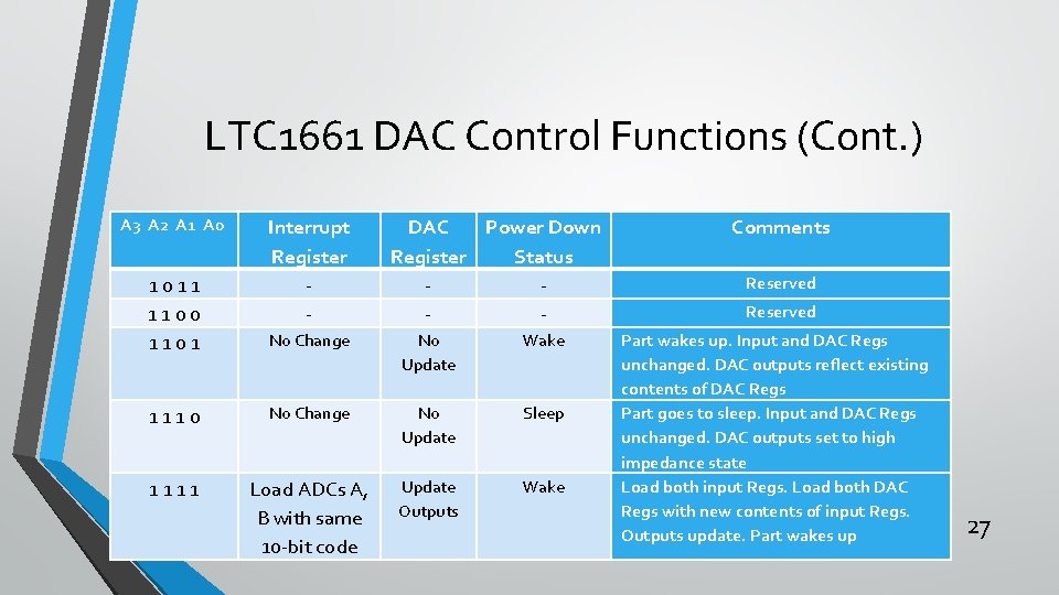
LTC 1661 DAC Control Functions (Cont. ) A 3 A 2 A 1 A 0 1011 1100 1101 Interrupt Register - DAC Power Down Register Status - No Change No Update Wake 1110 No Change No Update Sleep 1111 Load ADCs A, B with same 10 -bit code Update Outputs Wake Comments Reserved Part wakes up. Input and DAC Regs unchanged. DAC outputs reflect existing contents of DAC Regs Part goes to sleep. Input and DAC Regs unchanged. DAC outputs set to high impedance state Load both input Regs. Load both DAC Regs with new contents of input Regs. Outputs update. Part wakes up 27

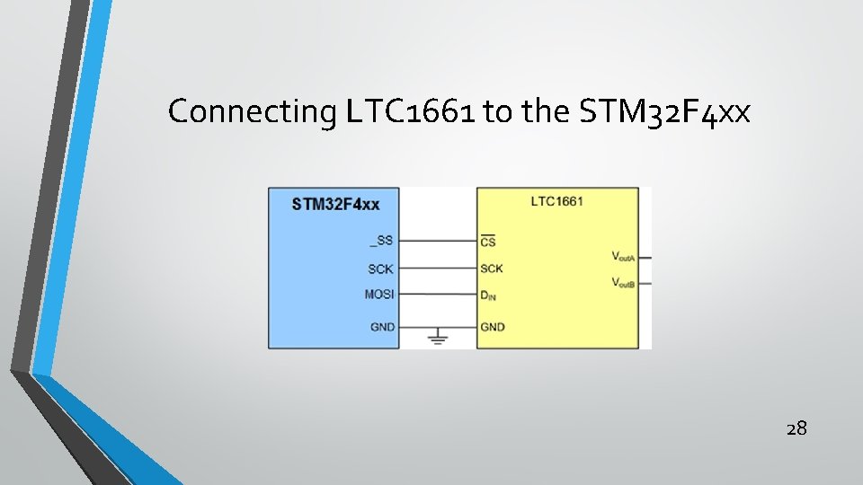
Connecting LTC 1661 to the STM 32 F 4 xx 28

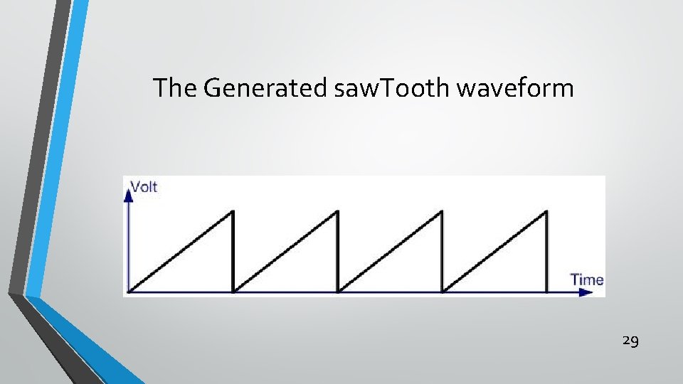
The Generated saw. Tooth waveform 29