Chapter 7 ADC DAC and Sensor Interfacing 1
- Slides: 43

Chapter 7 ADC, DAC, and Sensor Interfacing 1

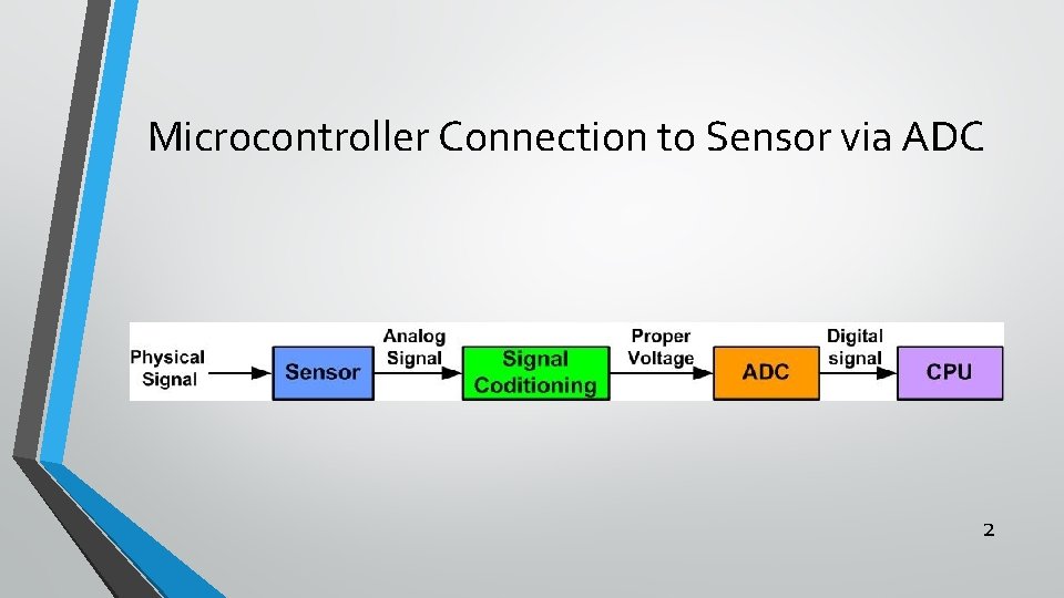
Microcontroller Connection to Sensor via ADC 2

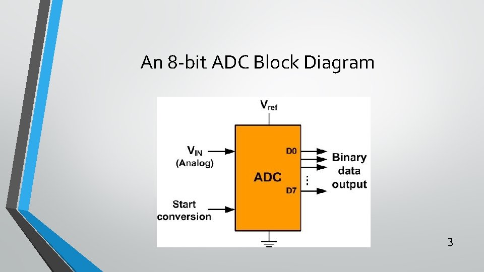
An 8 -bit ADC Block Diagram 3

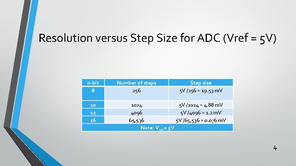
Resolution versus Step Size for ADC (Vref = 5 V) n-bit 8 10 12 16 Number of steps 256 Step size 5 V /256 = 19. 53 m. V 1024 5 V /1024 = 4. 88 m. V 4096 5 V /4096 = 1. 2 m. V 65, 536 5 V /65, 536 = 0. 076 m. V Note: Vref = 5 V 4

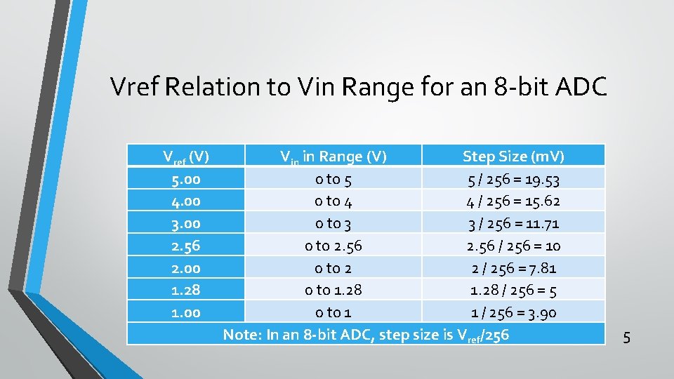
Vref Relation to Vin Range for an 8 -bit ADC Vref (V) 5. 00 4. 00 3. 00 2. 56 2. 00 1. 28 1. 00 Vin in Range (V) Step Size (m. V) 0 to 5 5 / 256 = 19. 53 0 to 4 4 / 256 = 15. 62 0 to 3 3 / 256 = 11. 71 0 to 2. 56 / 256 = 10 0 to 2 2 / 256 = 7. 81 0 to 1. 28 / 256 = 5 0 to 1 1 / 256 = 3. 90 Note: In an 8 -bit ADC, step size is Vref/256 5

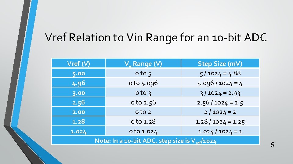
Vref Relation to Vin Range for an 10 -bit ADC Vref (V) 5. 00 4. 96 3. 00 2. 56 2. 00 1. 28 1. 024 Vin. Range (V) Step Size (m. V) 0 to 5 5 / 1024 = 4. 88 0 to 4. 096 / 1024 = 4 0 to 3 3 / 1024 = 2. 93 0 to 2. 56 / 1024 = 2. 5 0 to 2 2 / 1024 = 2 0 to 1. 28 / 1024 = 1. 25 0 to 1. 024 / 1024 = 1 Note: In a 10 -bit ADC, step size is Vref/1024 6

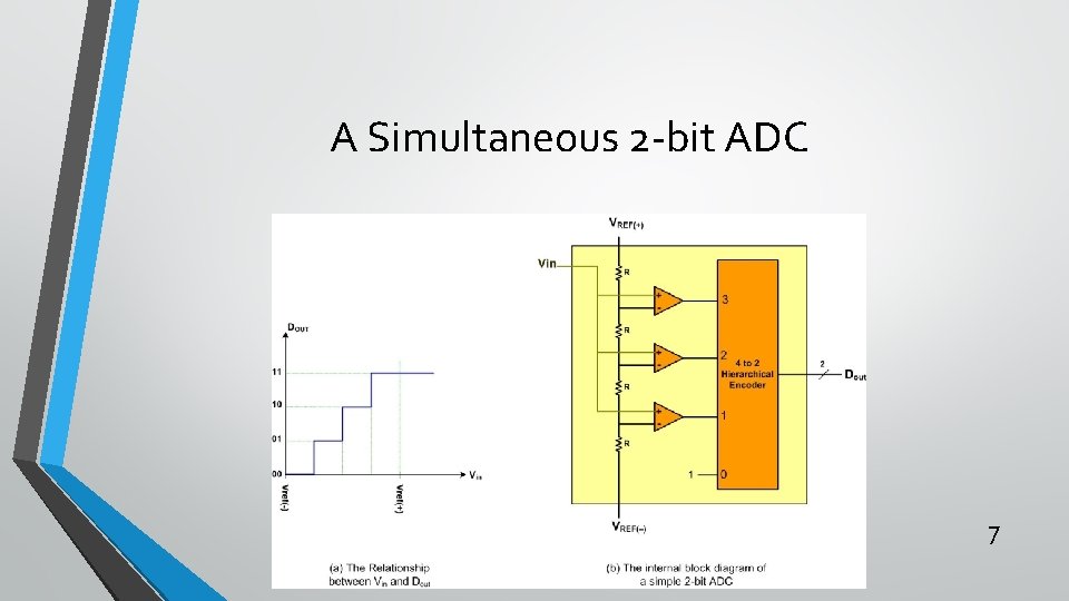
A Simultaneous 2 -bit ADC 7

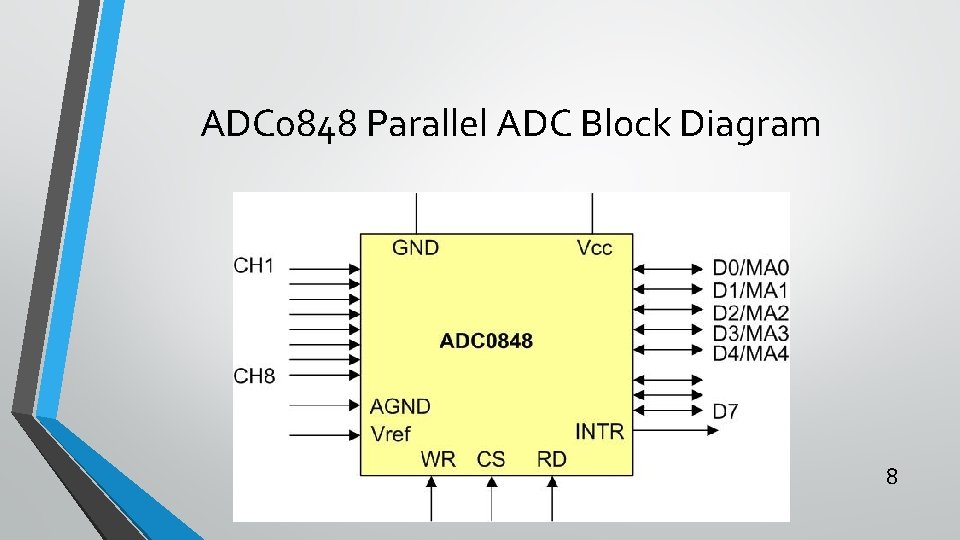
ADC 0848 Parallel ADC Block Diagram 8

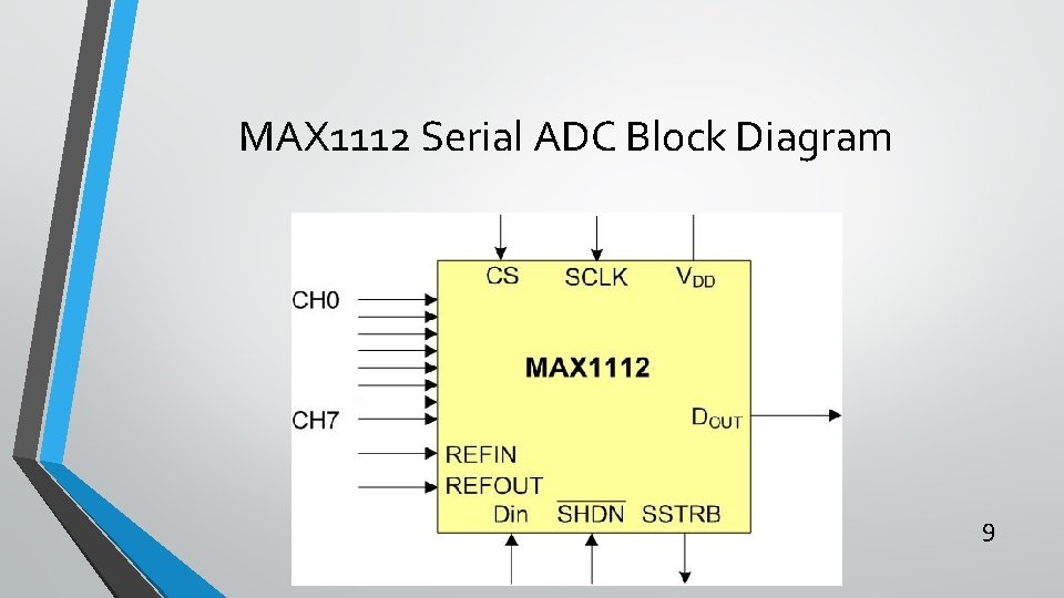
MAX 1112 Serial ADC Block Diagram 9

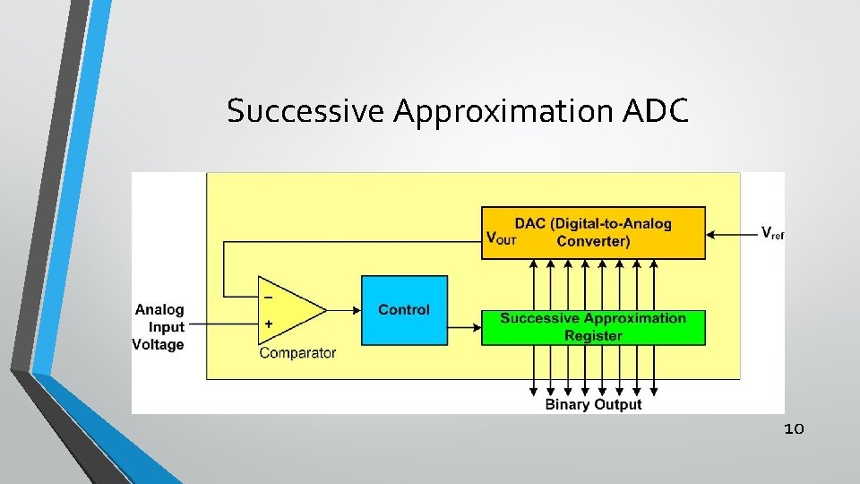
Successive Approximation ADC 10

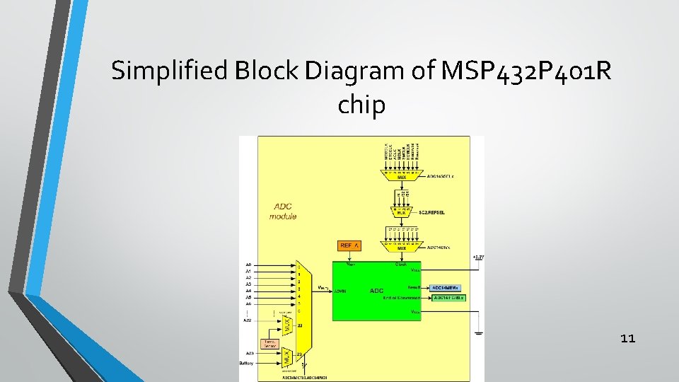
Simplified Block Diagram of MSP 432 P 401 R chip 11

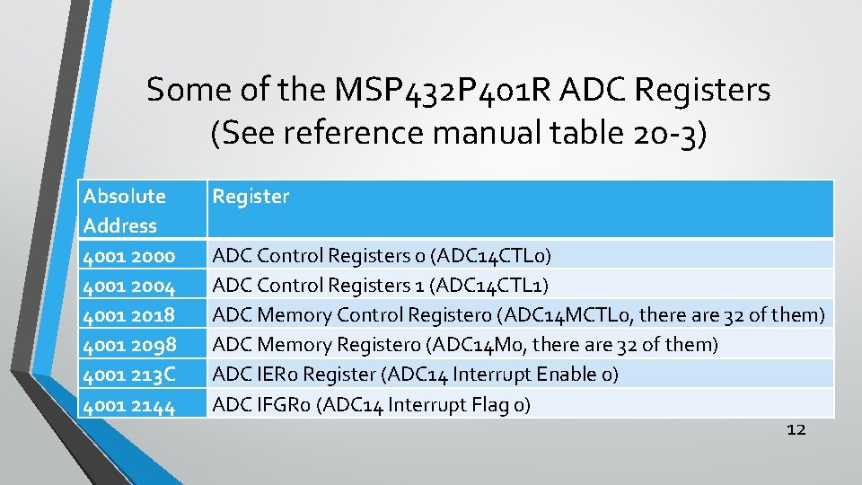
Some of the MSP 432 P 401 R ADC Registers (See reference manual table 20 -3) Absolute Address 4001 2000 4001 2004 4001 2018 4001 2098 4001 213 C 4001 2144 Register ADC Control Registers 0 (ADC 14 CTL 0) ADC Control Registers 1 (ADC 14 CTL 1) ADC Memory Control Register 0 (ADC 14 MCTL 0, there are 32 of them) ADC Memory Register 0 (ADC 14 M 0, there are 32 of them) ADC IER 0 Register (ADC 14 Interrupt Enable 0) ADC IFGR 0 (ADC 14 Interrupt Flag 0) 12

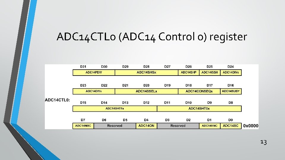
ADC 14 CTL 0 (ADC 14 Control 0) register 13

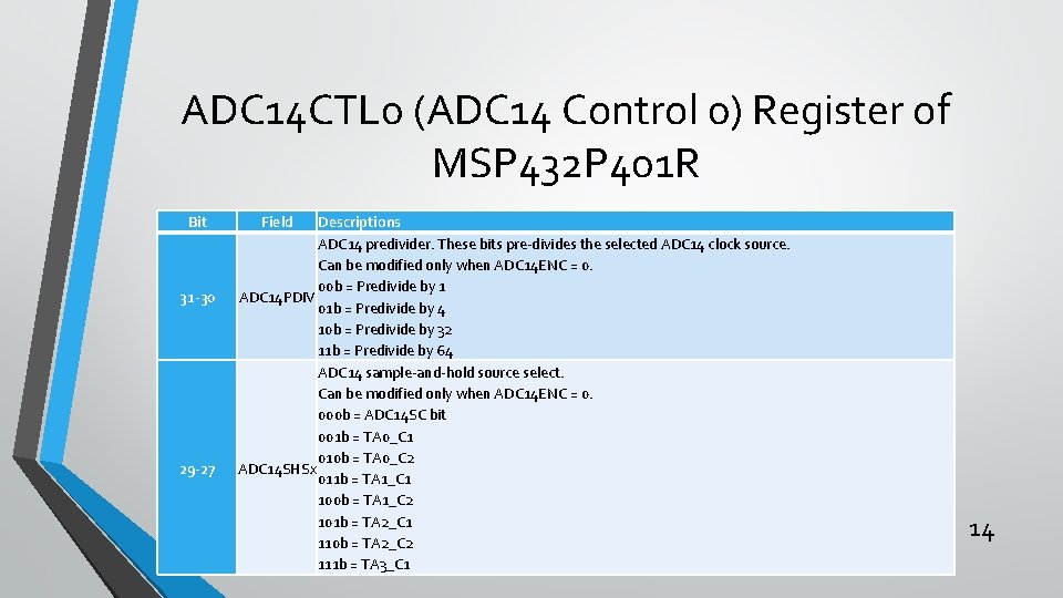
ADC 14 CTL 0 (ADC 14 Control 0) Register of MSP 432 P 401 R Bit 31 -30 29 -27 Field Descriptions ADC 14 predivider. These bits pre-divides the selected ADC 14 clock source. Can be modified only when ADC 14 ENC = 0. 00 b = Predivide by 1 ADC 14 PDIV 01 b = Predivide by 4 10 b = Predivide by 32 11 b = Predivide by 64 ADC 14 sample-and-hold source select. Can be modified only when ADC 14 ENC = 0. 000 b = ADC 14 SC bit 001 b = TA 0_C 1 010 b = TA 0_C 2 ADC 14 SHSx 011 b = TA 1_C 1 100 b = TA 1_C 2 101 b = TA 2_C 1 110 b = TA 2_C 2 111 b = TA 3_C 1 14

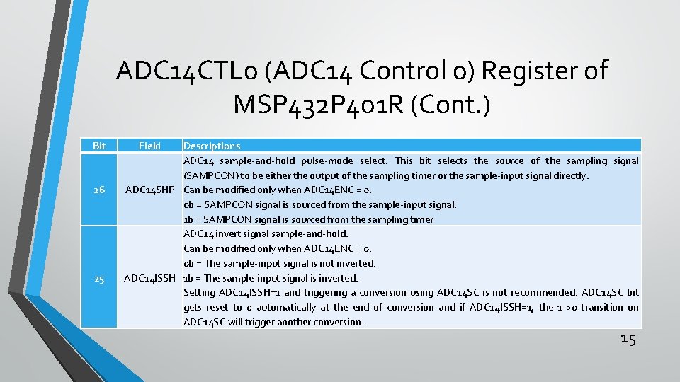
ADC 14 CTL 0 (ADC 14 Control 0) Register of MSP 432 P 401 R (Cont. ) Bit 26 25 Field Descriptions ADC 14 sample-and-hold pulse-mode select. This bit selects the source of the sampling signal (SAMPCON) to be either the output of the sampling timer or the sample-input signal directly. ADC 14 SHP Can be modified only when ADC 14 ENC = 0. 0 b = SAMPCON signal is sourced from the sample-input signal. 1 b = SAMPCON signal is sourced from the sampling timer ADC 14 invert signal sample-and-hold. Can be modified only when ADC 14 ENC = 0. 0 b = The sample-input signal is not inverted. ADC 14 ISSH 1 b = The sample-input signal is inverted. Setting ADC 14 ISSH=1 and triggering a conversion using ADC 14 SC is not recommended. ADC 14 SC bit gets reset to 0 automatically at the end of conversion and if ADC 14 ISSH=1, the 1 ->0 transition on ADC 14 SC will trigger another conversion. 15

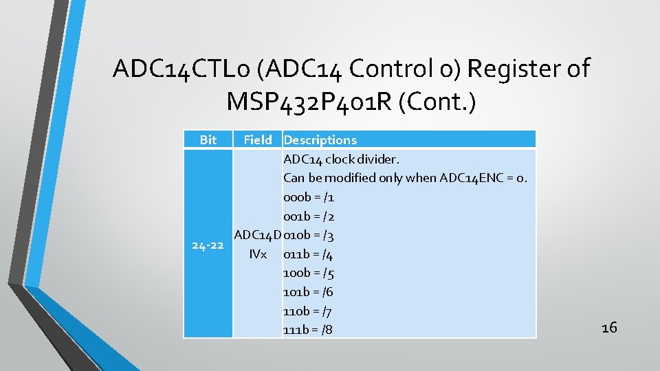
ADC 14 CTL 0 (ADC 14 Control 0) Register of MSP 432 P 401 R (Cont. ) Bit Field Descriptions ADC 14 clock divider. Can be modified only when ADC 14 ENC = 0. 000 b = /1 001 b = /2 ADC 14 D 010 b = /3 24 -22 IVx 011 b = /4 100 b = /5 101 b = /6 110 b = /7 111 b = /8 16

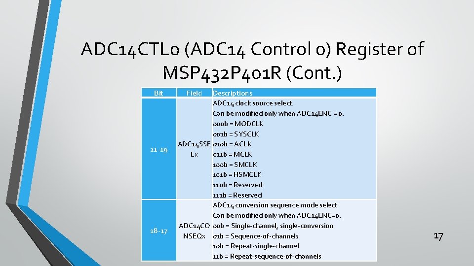
ADC 14 CTL 0 (ADC 14 Control 0) Register of MSP 432 P 401 R (Cont. ) Bit 21 -19 18 -17 Field Descriptions ADC 14 clock source select. Can be modified only when ADC 14 ENC = 0. 000 b = MODCLK 001 b = SYSCLK ADC 14 SSE 010 b = ACLK Lx 011 b = MCLK 100 b = SMCLK 101 b = HSMCLK 110 b = Reserved 111 b = Reserved ADC 14 conversion sequence mode select Can be modified only when ADC 14 ENC=0. ADC 14 CO 00 b = Single-channel, single-conversion NSEQx 01 b = Sequence-of-channels 10 b = Repeat-single-channel 11 b = Repeat-sequence-of-channels 17

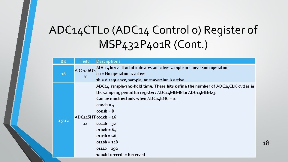
ADC 14 CTL 0 (ADC 14 Control 0) Register of MSP 432 P 401 R (Cont. ) Bit 16 15 -12 Field Descriptions ADC 14 busy. This bit indicates an active sample or conversion operation. ADC 14 BUS 0 b = No operation is active. Y 1 b = A sequence, sample, or conversion is active ADC 14 sample-and-hold time. These bits define the number of ADC 14 CLK cycles in the sampling period for registers ADC 14 MEM 8 to ADC 14 MEM 23. Can be modified only when ADC 14 ENC = 0. 0000 b = 4 0001 b = 8 ADC 14 SHT 0010 b = 16 1 x 0011 b = 32 0100 b = 64 0101 b = 96 0110 b = 128 0111 b = 192 1000 b to 1111 b = Reserved 18

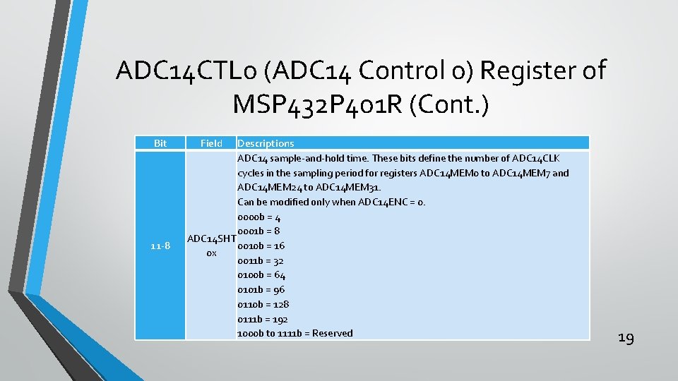
ADC 14 CTL 0 (ADC 14 Control 0) Register of MSP 432 P 401 R (Cont. ) Bit 11 -8 Field Descriptions ADC 14 sample-and-hold time. These bits define the number of ADC 14 CLK cycles in the sampling period for registers ADC 14 MEM 0 to ADC 14 MEM 7 and ADC 14 MEM 24 to ADC 14 MEM 31. Can be modified only when ADC 14 ENC = 0. 0000 b = 4 0001 b = 8 ADC 14 SHT 0010 b = 16 0 x 0011 b = 32 0100 b = 64 0101 b = 96 0110 b = 128 0111 b = 192 1000 b to 1111 b = Reserved 19

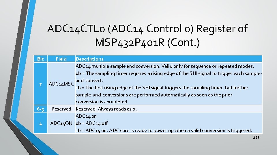
ADC 14 CTL 0 (ADC 14 Control 0) Register of MSP 432 P 401 R (Cont. ) Bit Field Descriptions ADC 14 multiple sample and conversion. Valid only for sequence or repeated modes. 0 b = The sampling timer requires a rising edge of the SHI signal to trigger each sampleand-convert. 7 ADC 14 MSC 1 b = The first rising edge of the SHI signal triggers the sampling timer, but further sample-and-conversions are performed automatically as soon as the prior conversion is completed 6 -5 Reserved. Always reads as 0. ADC 14 on 4 ADC 14 ON 0 b = ADC 14 off 1 b = ADC 14 on. ADC core is ready to power up when a valid conversion is triggered. 20

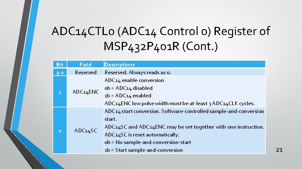
ADC 14 CTL 0 (ADC 14 Control 0) Register of MSP 432 P 401 R (Cont. ) Bit 3 -2 1 0 Field Reserved Descriptions Reserved. Always reads as 0. ADC 14 enable conversion 0 b = ADC 14 disabled ADC 14 ENC 1 b = ADC 14 enabled ADC 14 ENC low pulse width must be at-least 3 ADC 14 CLK cycles. ADC 14 start conversion. Software-controlled sample-and-conversion start. ADC 14 SC and ADC 14 ENC may be set together with one instruction. ADC 14 SC is reset automatically. 0 b = No sample-and-conversion-start 1 b = Start sample-and-conversion 21

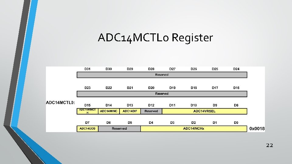
ADC 14 MCTL 0 Register 22

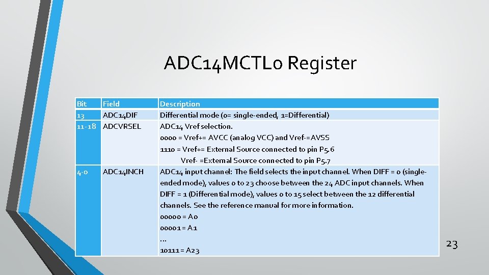
ADC 14 MCTL 0 Register Bit Field 13 ADC 14 DIF 11 -18 ADCVRSEL 4 -0 ADC 14 INCH Description Differential mode (0= single-ended, 1=Differential) ADC 14 Vref selection. 0000 = Vref+= AVCC (analog VCC) and Vref-=AVSS 1110 = Vref+= External Source connected to pin P 5. 6 Vref- =External Source connected to pin P 5. 7 ADC 14 input channel: The field selects the input channel. When DIFF = 0 (singleended mode), values 0 to 23 choose between the 24 ADC input channels. When DIFF = 1 (Differential mode), values 0 to 15 select between the 12 differential channels. See the reference manual for more information. 00000 = A 0 00001 = A 1 … 10111 = A 23 23

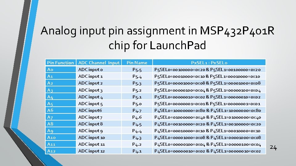
Analog input pin assignment in MSP 432 P 401 R chip for Launch. Pad Pin Function A 0 A 1 A 2 A 3 A 4 A 5 A 6 A 7 A 8 A 9 A 10 A 11 A 12 ADC Channel Input ADC input 0 ADC input 1 ADC input 2 ADC input 3 ADC input 4 ADC input 5 ADC input 6 ADC input 7 ADC input 8 ADC input 9 ADC input 10 ADC input 11 ADC input 12 Pin Name P 5. 5 P 5. 4 P 5. 3 P 5. 2 P 5. 1 P 5. 0 P 4. 7 P 4. 6 P 4. 5 P 4. 4 P 4. 3 P 4. 2 P 4. 1 Px. SEL 1 : Px. SEL 0 P 5 SEL 0=00100000=0 x 20 & P 5 SEL 1=00100000=0 x 20 P 5 SEL 0=00010000=0 x 10 & P 5 SEL 1=00010000=0 x 10 P 5 SEL 0=00001000=0 x 08 & P 5 SEL 1=00001000=0 x 08 P 5 SEL 0=00000100=0 x 04 & P 5 SEL 1=00000100=0 x 04 P 5 SEL 0=00000010=0 x 02 & P 5 SEL 1=00000010=0 x 02 P 5 SEL 0=00000001=0 x 01 & P 5 SEL 1=00000001=0 x 01 P 4 SEL 0=10000000=0 x 80 & P 4 SEL 1=10000000=0 x 80 P 4 SEL 0=01000000=0 x 40 & P 4 SEL 1=01000000=0 x 40 P 4 SEL 0=00100000=0 x 20 & P 4 SEL 1=00100000=0 x 20 P 4 SEL 0=00010000=0 x 10 & P 4 SEL 1=00010000=0 x 10 P 4 SEL 0=00001000=0 x 08 & P 4 SEL 1=00001000=0 x 08 P 4 SEL 0=00000100=0 x 04 & P 4 SEL 1=00000100=0 x 04 P 4 SEL 0=00000010=0 x 02 & P 4 SEL 1=00000010=0 x 02 24

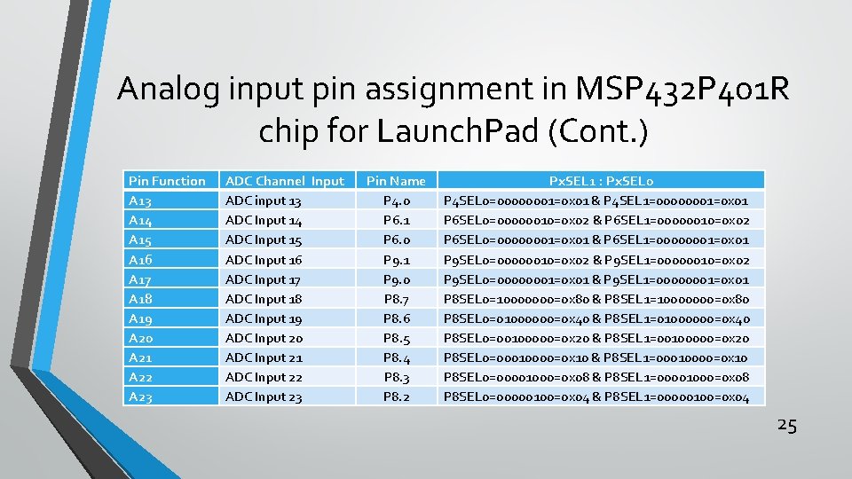
Analog input pin assignment in MSP 432 P 401 R chip for Launch. Pad (Cont. ) Pin Function A 13 A 14 A 15 A 16 A 17 A 18 A 19 A 20 A 21 A 22 A 23 ADC Channel Input ADC input 13 ADC Input 14 ADC Input 15 ADC Input 16 ADC Input 17 ADC Input 18 ADC Input 19 ADC Input 20 ADC Input 21 ADC Input 22 ADC Input 23 Pin Name P 4. 0 P 6. 1 P 6. 0 P 9. 1 P 9. 0 P 8. 7 P 8. 6 P 8. 5 P 8. 4 P 8. 3 P 8. 2 Px. SEL 1 : Px. SEL 0 P 4 SEL 0=00000001=0 x 01 & P 4 SEL 1=00000001=0 x 01 P 6 SEL 0=00000010=0 x 02 & P 6 SEL 1=00000010=0 x 02 P 6 SEL 0=00000001=0 x 01 & P 6 SEL 1=00000001=0 x 01 P 9 SEL 0=00000010=0 x 02 & P 9 SEL 1=00000010=0 x 02 P 9 SEL 0=00000001=0 x 01 & P 9 SEL 1=00000001=0 x 01 P 8 SEL 0=10000000=0 x 80 & P 8 SEL 1=10000000=0 x 80 P 8 SEL 0=01000000=0 x 40 & P 8 SEL 1=01000000=0 x 40 P 8 SEL 0=00100000=0 x 20 & P 8 SEL 1=00100000=0 x 20 P 8 SEL 0=00010000=0 x 10 & P 8 SEL 1=00010000=0 x 10 P 8 SEL 0=00001000=0 x 08 & P 8 SEL 1=00001000=0 x 08 P 8 SEL 0=00000100=0 x 04 & P 8 SEL 1=00000100=0 x 04 25

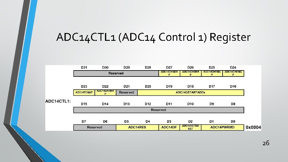
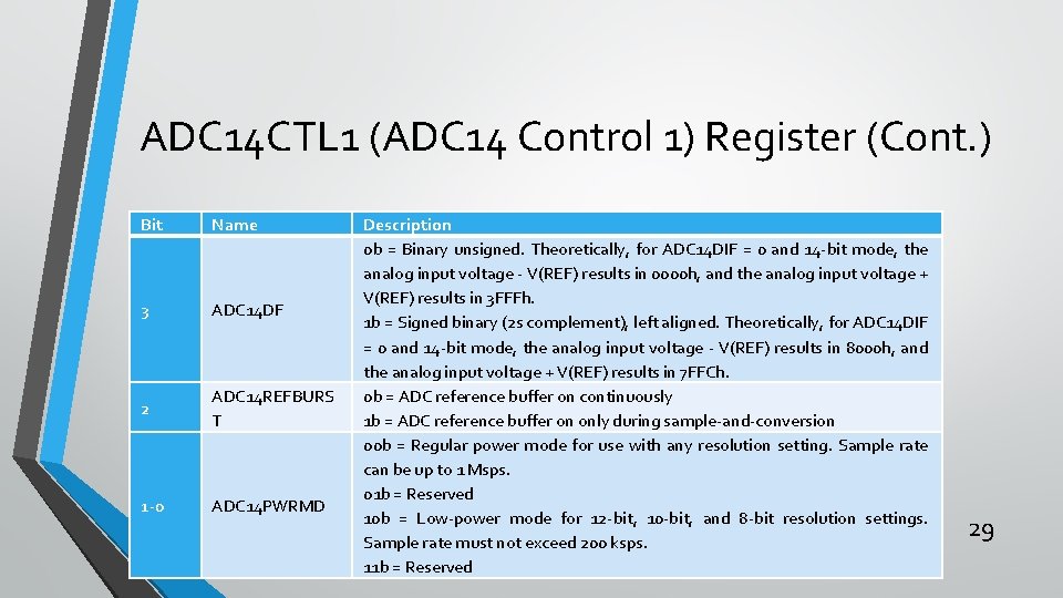
ADC 14 CTL 1 (ADC 14 Control 1) Register 26

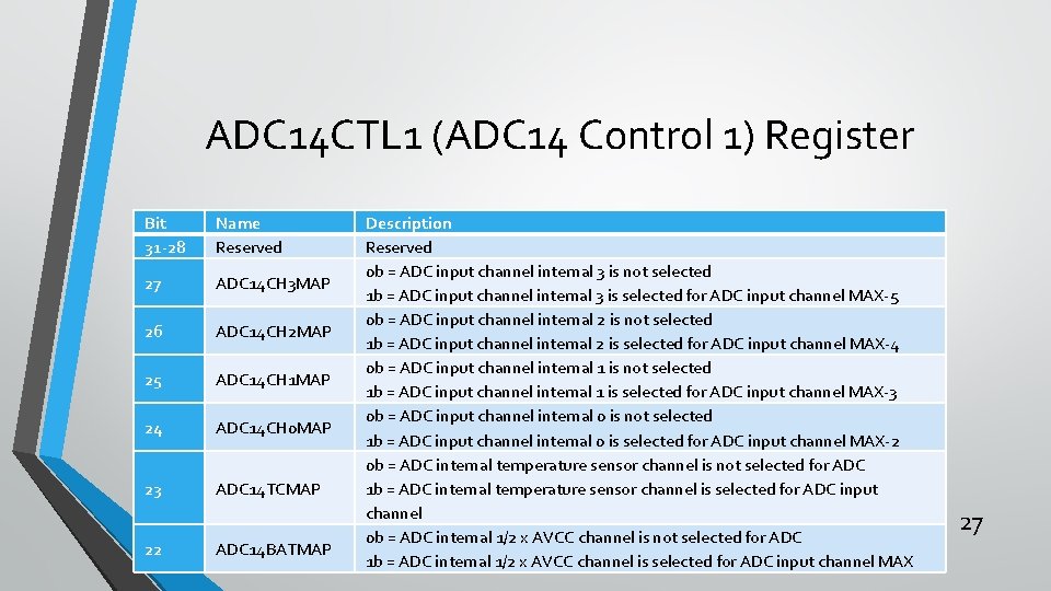
ADC 14 CTL 1 (ADC 14 Control 1) Register Bit 31 -28 Name Reserved 27 ADC 14 CH 3 MAP 26 ADC 14 CH 2 MAP 25 ADC 14 CH 1 MAP 24 ADC 14 CH 0 MAP 23 ADC 14 TCMAP 22 ADC 14 BATMAP Description Reserved 0 b = ADC input channel internal 3 is not selected 1 b = ADC input channel internal 3 is selected for ADC input channel MAX-5 0 b = ADC input channel internal 2 is not selected 1 b = ADC input channel internal 2 is selected for ADC input channel MAX-4 0 b = ADC input channel internal 1 is not selected 1 b = ADC input channel internal 1 is selected for ADC input channel MAX-3 0 b = ADC input channel internal 0 is not selected 1 b = ADC input channel internal 0 is selected for ADC input channel MAX-2 0 b = ADC internal temperature sensor channel is not selected for ADC 1 b = ADC internal temperature sensor channel is selected for ADC input channel 0 b = ADC internal 1/2 x AVCC channel is not selected for ADC 1 b = ADC internal 1/2 x AVCC channel is selected for ADC input channel MAX 27

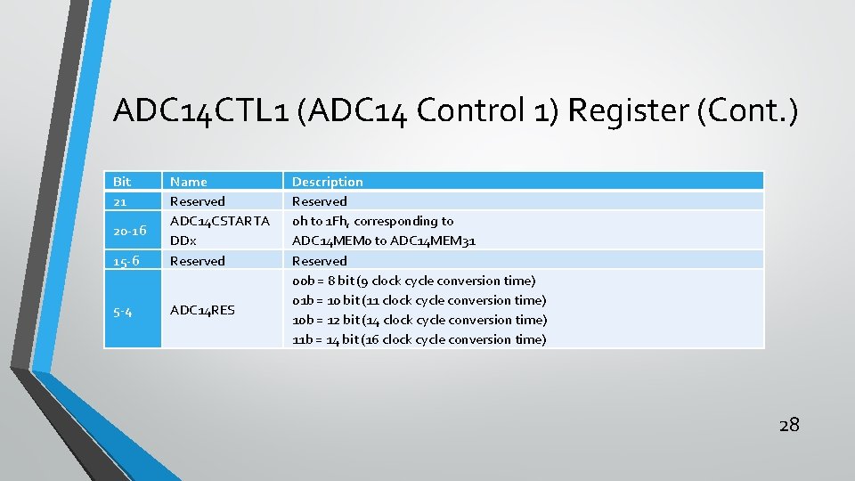
ADC 14 CTL 1 (ADC 14 Control 1) Register (Cont. ) Bit 21 15 -6 Name Reserved ADC 14 CSTARTA DDx Reserved 5 -4 ADC 14 RES 20 -16 Description Reserved 0 h to 1 Fh, corresponding to ADC 14 MEM 0 to ADC 14 MEM 31 Reserved 00 b = 8 bit (9 clock cycle conversion time) 01 b = 10 bit (11 clock cycle conversion time) 10 b = 12 bit (14 clock cycle conversion time) 11 b = 14 bit (16 clock cycle conversion time) 28

ADC 14 CTL 1 (ADC 14 Control 1) Register (Cont. ) Bit Name 3 ADC 14 DF 2 ADC 14 REFBURS T 1 -0 ADC 14 PWRMD Description 0 b = Binary unsigned. Theoretically, for ADC 14 DIF = 0 and 14 -bit mode, the analog input voltage - V(REF) results in 0000 h, and the analog input voltage + V(REF) results in 3 FFFh. 1 b = Signed binary (2 s complement), left aligned. Theoretically, for ADC 14 DIF = 0 and 14 -bit mode, the analog input voltage - V(REF) results in 8000 h, and the analog input voltage + V(REF) results in 7 FFCh. 0 b = ADC reference buffer on continuously 1 b = ADC reference buffer on only during sample-and-conversion 00 b = Regular power mode for use with any resolution setting. Sample rate can be up to 1 Msps. 01 b = Reserved 10 b = Low-power mode for 12 -bit, 10 -bit, and 8 -bit resolution settings. Sample rate must not exceed 200 ksps. 11 b = Reserved 29

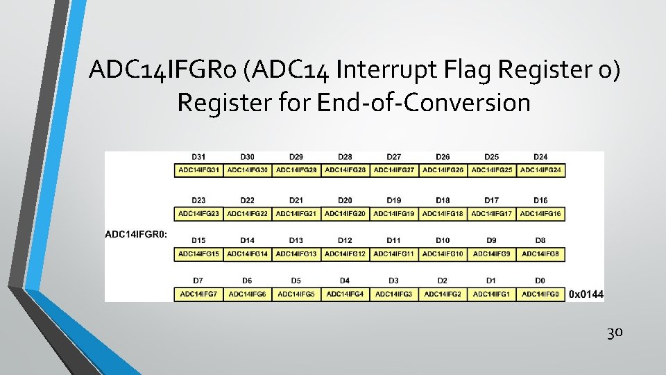
ADC 14 IFGR 0 (ADC 14 Interrupt Flag Register 0) Register for End-of-Conversion 30

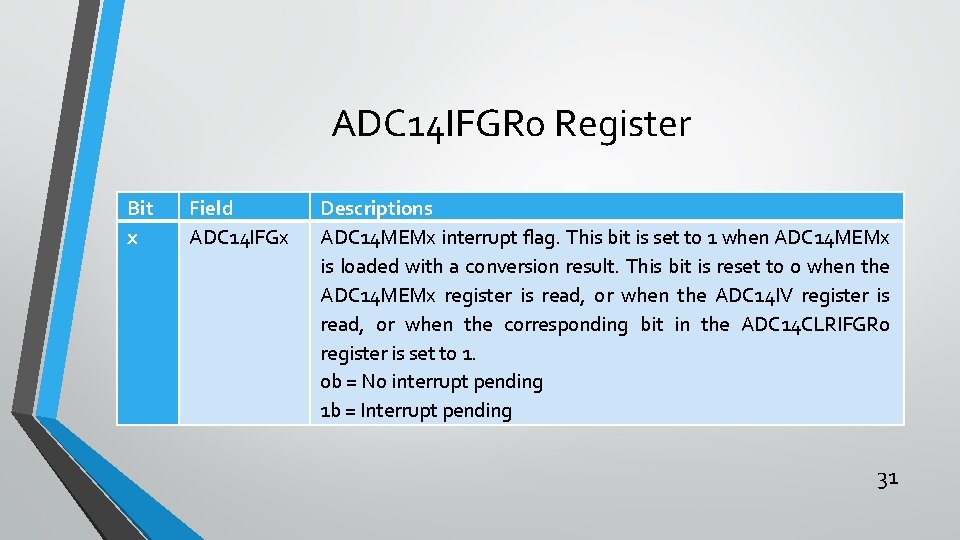
ADC 14 IFGR 0 Register Bit x Field ADC 14 IFGx Descriptions ADC 14 MEMx interrupt flag. This bit is set to 1 when ADC 14 MEMx is loaded with a conversion result. This bit is reset to 0 when the ADC 14 MEMx register is read, or when the ADC 14 IV register is read, or when the corresponding bit in the ADC 14 CLRIFGR 0 register is set to 1. 0 b = No interrupt pending 1 b = Interrupt pending 31

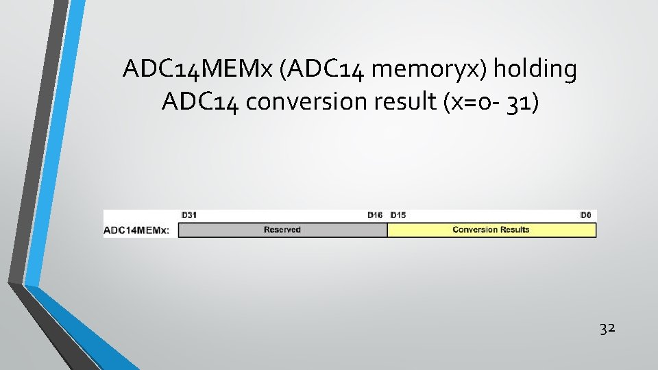
ADC 14 MEMx (ADC 14 memoryx) holding ADC 14 conversion result (x=0 - 31) 32

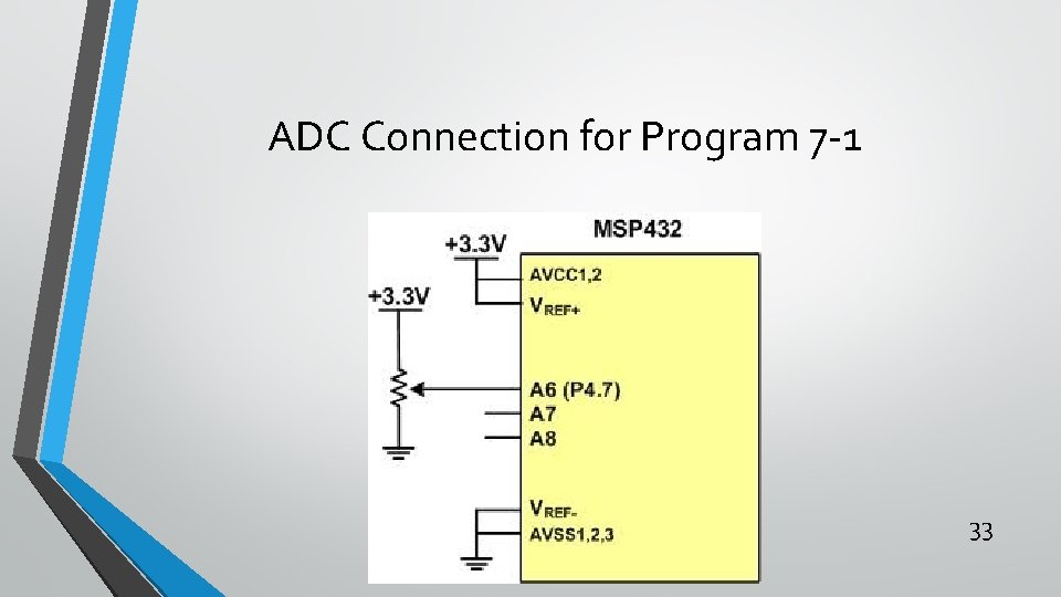
ADC Connection for Program 7 -1 33

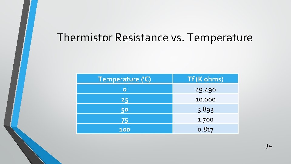
Thermistor Resistance vs. Temperature ('C) 0 25 50 75 100 Tf (K ohms) 29. 490 10. 000 3. 893 1. 700 0. 817 34

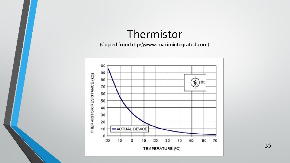
Thermistor (Copied from http: //www. maximintegrated. com) 35

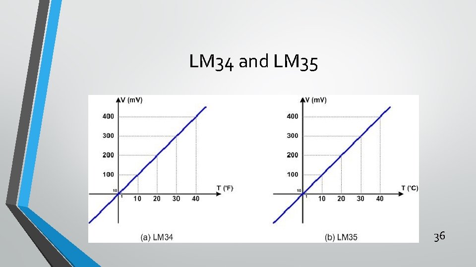
LM 34 and LM 35 36

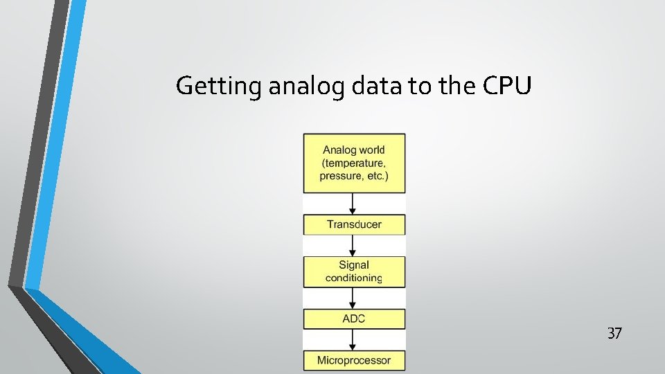
Getting analog data to the CPU 37

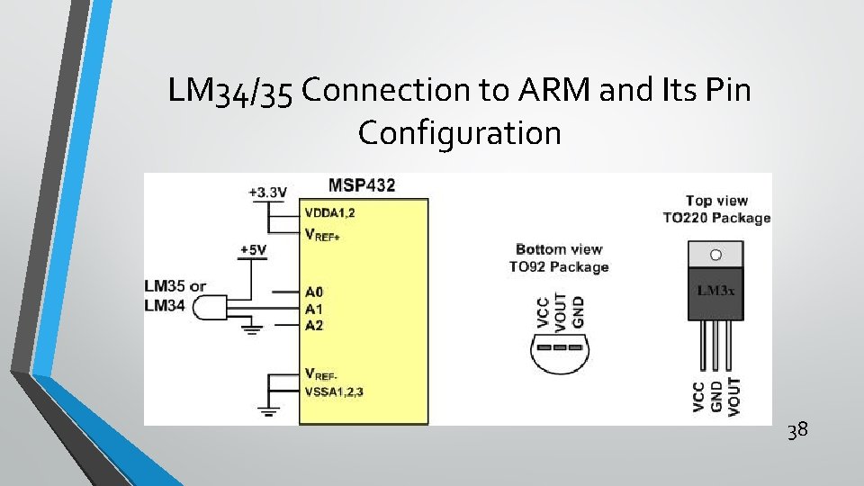
LM 34/35 Connection to ARM and Its Pin Configuration 38

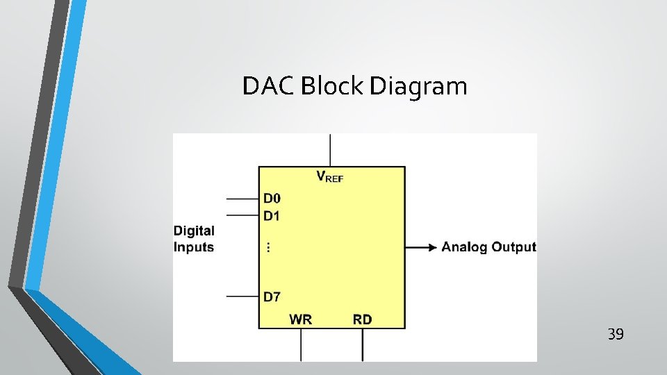
DAC Block Diagram 39

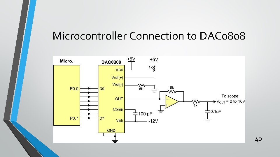
Microcontroller Connection to DAC 0808 40

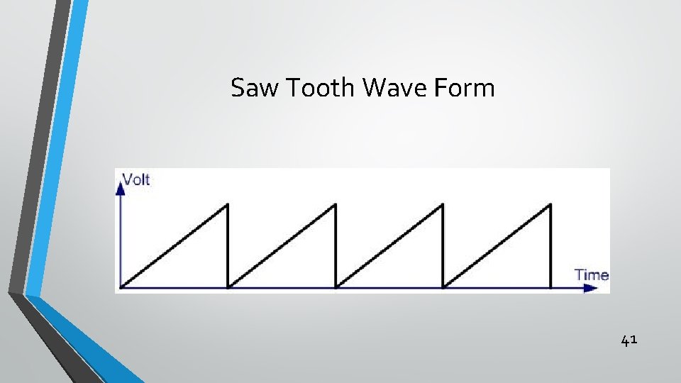
Saw Tooth Wave Form 41

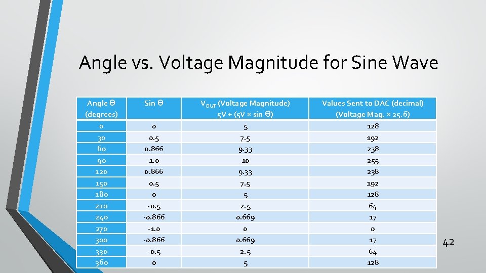
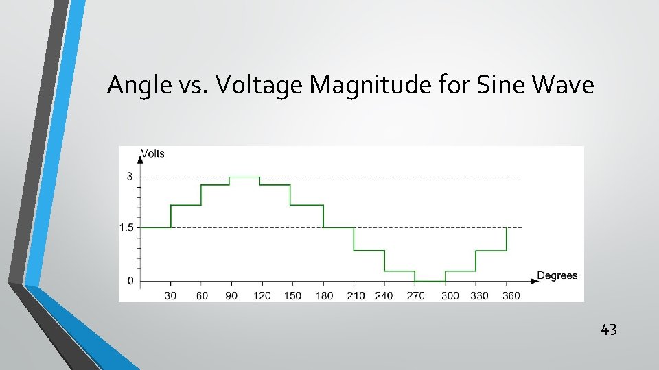
Angle vs. Voltage Magnitude for Sine Wave Angle Ɵ (degrees) 0 30 60 90 120 150 180 210 240 270 300 330 360 Sin Ɵ 0 0. 5 0. 866 1. 0 0. 866 0. 5 0 -0. 5 -0. 866 -1. 0 -0. 866 -0. 5 0 VOUT (Voltage Magnitude) 5 V + (5 V × sin Ɵ) 5 7. 5 9. 33 10 9. 33 7. 5 5 2. 5 0. 669 0 0. 669 2. 5 5 Values Sent to DAC (decimal) (Voltage Mag. × 25. 6) 128 192 238 255 238 192 128 64 17 0 17 64 128 42

Angle vs. Voltage Magnitude for Sine Wave 43