Chapter 7 ADC DAC and Sensor Interfacing STM

![Bit 4: 3 RES[1: 0]: Data resolution These bits are written by software to Bit 4: 3 RES[1: 0]: Data resolution These bits are written by software to](https://slidetodoc.com/presentation_image_h2/a79a445fd022673d48d8e71d73aa3163/image-15.jpg)
![Bit 4 -0 Description ADC Channel Input Selection AWDCH[4: 0] 0 x 00 0 Bit 4 -0 Description ADC Channel Input Selection AWDCH[4: 0] 0 x 00 0](https://slidetodoc.com/presentation_image_h2/a79a445fd022673d48d8e71d73aa3163/image-18.jpg)
![Bits 2 y: 2 y+1 MODERy[1: 0]: Port x configuration bits (y = 0. Bits 2 y: 2 y+1 MODERy[1: 0]: Port x configuration bits (y = 0.](https://slidetodoc.com/presentation_image_h2/a79a445fd022673d48d8e71d73aa3163/image-20.jpg)
- Slides: 37

Chapter 7: ADC, DAC, and Sensor Interfacing STM 32 F 0 Arm Cortex M 0 Programming for Embedded Systems Using C Language with STM 32 F 0 Nucleo Board by Mazidi, et al. www. microdigitaled. com

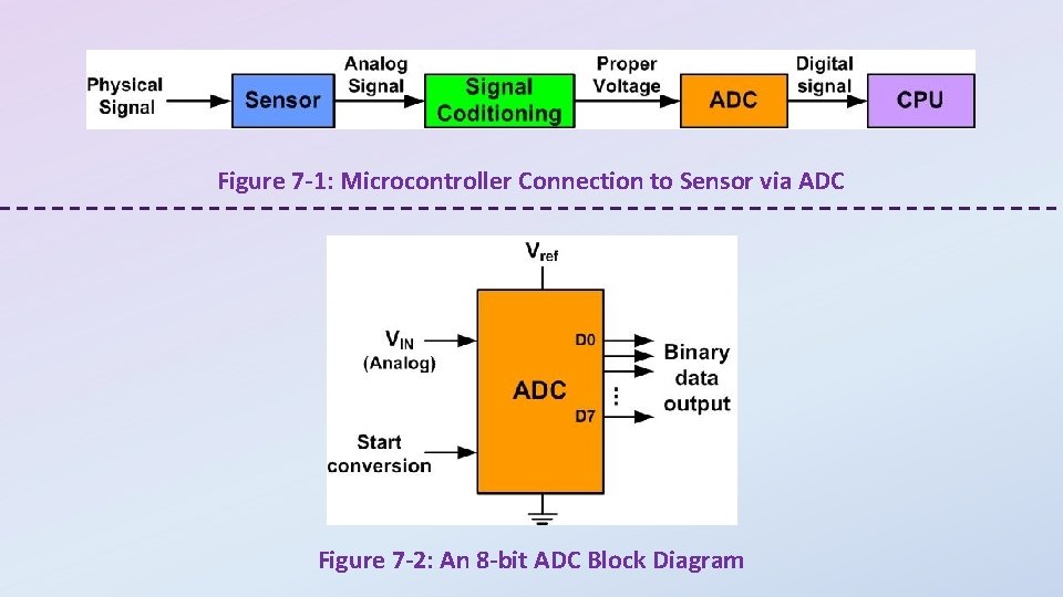
Figure 7 -1: Microcontroller Connection to Sensor via ADC Figure 7 -2: An 8 -bit ADC Block Diagram

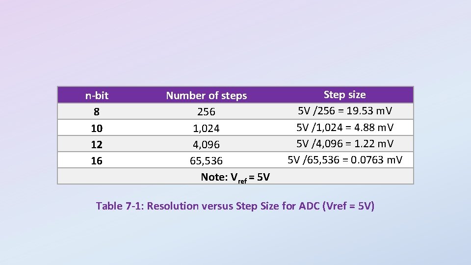
n-bit 8 10 12 16 Number of steps 256 1, 024 4, 096 65, 536 Note: Vref = 5 V Step size 5 V /256 = 19. 53 m. V 5 V /1, 024 = 4. 88 m. V 5 V /4, 096 = 1. 22 m. V 5 V /65, 536 = 0. 0763 m. V Table 7 -1: Resolution versus Step Size for ADC (Vref = 5 V)

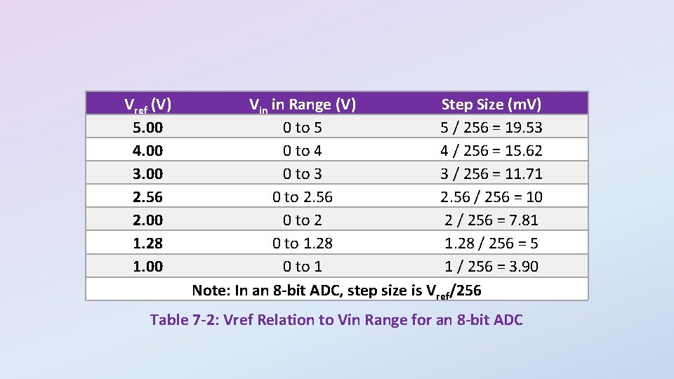
Vref (V) 5. 00 4. 00 3. 00 2. 56 2. 00 1. 28 1. 00 Vin in Range (V) Step Size (m. V) 0 to 5 5 / 256 = 19. 53 0 to 4 4 / 256 = 15. 62 0 to 3 3 / 256 = 11. 71 0 to 2. 56 / 256 = 10 0 to 2 2 / 256 = 7. 81 0 to 1. 28 / 256 = 5 0 to 1 1 / 256 = 3. 90 Note: In an 8 -bit ADC, step size is Vref/256 Table 7 -2: Vref Relation to Vin Range for an 8 -bit ADC

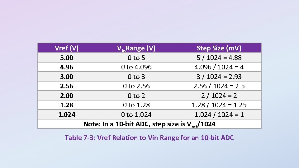
Vref (V) 5. 00 4. 96 3. 00 2. 56 2. 00 1. 28 1. 024 Vin. Range (V) Step Size (m. V) 0 to 5 5 / 1024 = 4. 88 0 to 4. 096 / 1024 = 4 0 to 3 3 / 1024 = 2. 93 0 to 2. 56 / 1024 = 2. 5 0 to 2 2 / 1024 = 2 0 to 1. 28 / 1024 = 1. 25 0 to 1. 024 / 1024 = 1 Note: In a 10 -bit ADC, step size is Vref/1024 Table 7 -3: Vref Relation to Vin Range for an 10 -bit ADC

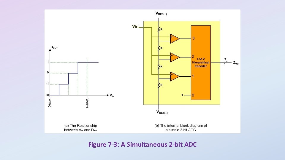
Figure 7 -3: A Simultaneous 2 -bit ADC

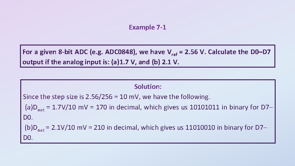
Example 7 -1 For a given 8 -bit ADC (e. g. ADC 0848), we have Vref = 2. 56 V. Calculate the D 0–D 7 output if the analog input is: (a)1. 7 V, and (b) 2. 1 V. Solution: Since the step size is 2. 56/256 = 10 m. V, we have the following. (a)Dout = 1. 7 V/10 m. V = 170 in decimal, which gives us 10101011 in binary for D 7– D 0. (b)Dout = 2. 1 V/10 m. V = 210 in decimal, which gives us 11010010 in binary for D 7– D 0.

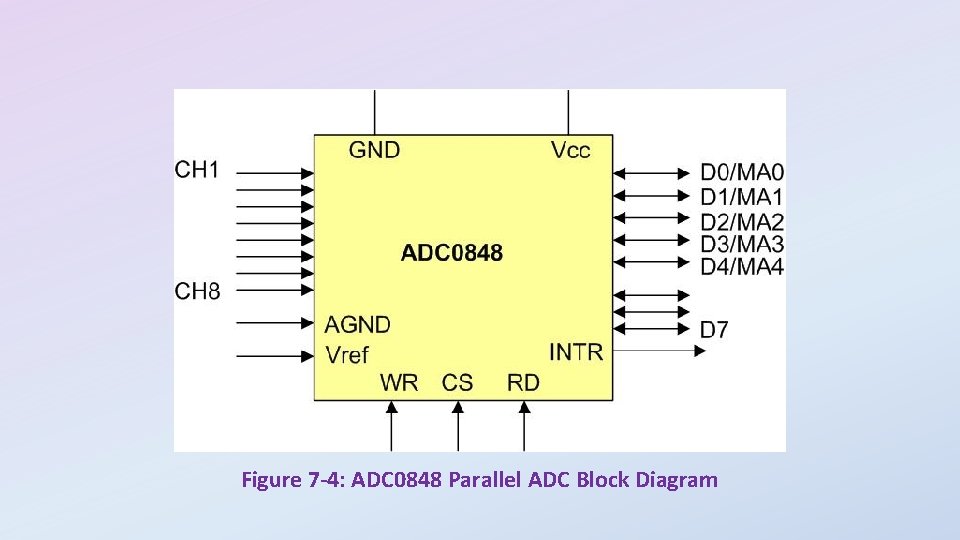
Figure 7 -4: ADC 0848 Parallel ADC Block Diagram

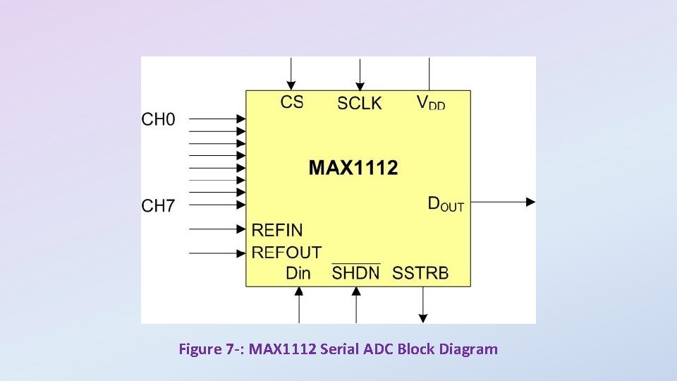
Figure 7 -: MAX 1112 Serial ADC Block Diagram

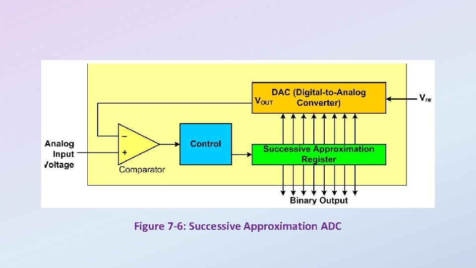
Figure 7 -6: Successive Approximation ADC

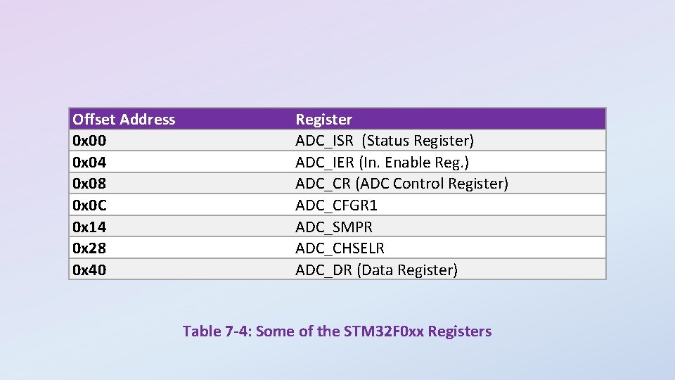
Offset Address 0 x 00 0 x 04 0 x 08 0 x 0 C 0 x 14 0 x 28 0 x 40 Register ADC_ISR (Status Register) ADC_IER (In. Enable Reg. ) ADC_CR (ADC Control Register) ADC_CFGR 1 ADC_SMPR ADC_CHSELR ADC_DR (Data Register) Table 7 -4: Some of the STM 32 F 0 xx Registers

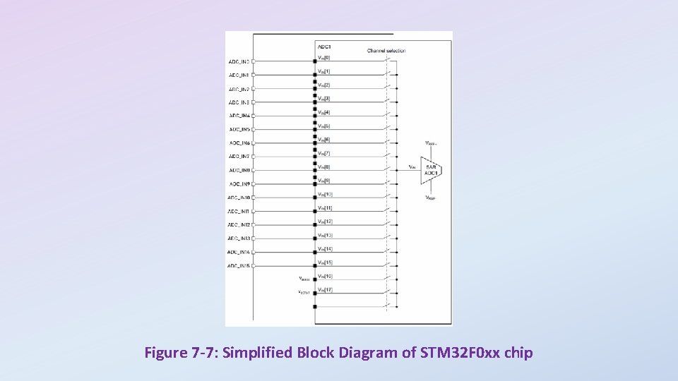
Figure 7 -7: Simplified Block Diagram of STM 32 F 0 xx chip

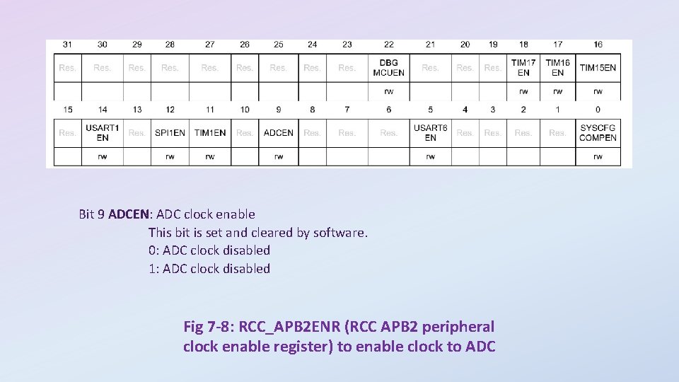
Bit 9 ADCEN: ADC clock enable This bit is set and cleared by software. 0: ADC clock disabled 1: ADC clock disabled Fig 7 -8: RCC_APB 2 ENR (RCC APB 2 peripheral clock enable register) to enable clock to ADC

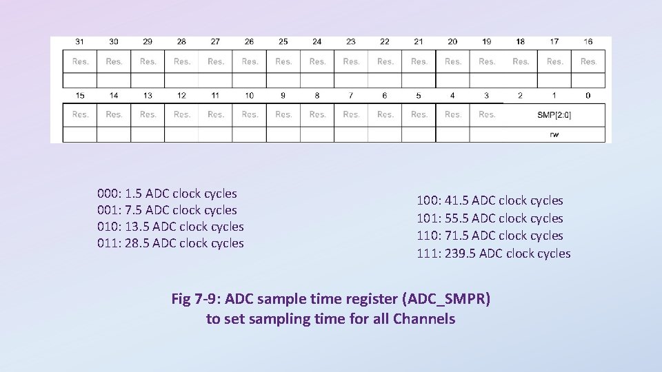
000: 1. 5 ADC clock cycles 001: 7. 5 ADC clock cycles 010: 13. 5 ADC clock cycles 011: 28. 5 ADC clock cycles 100: 41. 5 ADC clock cycles 101: 55. 5 ADC clock cycles 110: 71. 5 ADC clock cycles 111: 239. 5 ADC clock cycles Fig 7 -9: ADC sample time register (ADC_SMPR) to set sampling time for all Channels
![Bit 4 3 RES1 0 Data resolution These bits are written by software to Bit 4: 3 RES[1: 0]: Data resolution These bits are written by software to](https://slidetodoc.com/presentation_image_h2/a79a445fd022673d48d8e71d73aa3163/image-15.jpg)
Bit 4: 3 RES[1: 0]: Data resolution These bits are written by software to select the resolution of the conversion. 00: 12 bits 01: 10 bits 10: 8 bits 11: 6 bits Bit 5 ALIGN: Data alignment This bit is set and cleared by software to select right or left alignment. 0: Right alignment 1: Left alignment Bit 13 CONT: Single / continuous conversion mode This bit is set and cleared by software. If it is set, conversion takes place continuously until it is cleared. 0: Single conversion mode 1: Continuous conversion mode Note: It is not possible to have both discontinuous mode and continuous mode enabled: it is forbidden to set both bits DISCEN=1 and CONT=1. Figure 7 -10 A: ADC_CFGR 1 (ADC configuration register 1). Not all bits are shown.

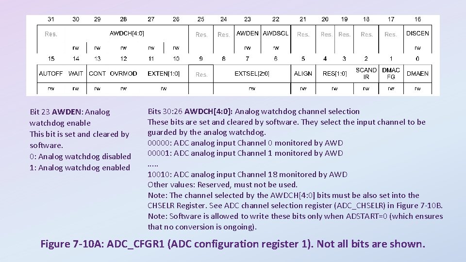
Bit 23 AWDEN: Analog watchdog enable This bit is set and cleared by software. 0: Analog watchdog disabled 1: Analog watchdog enabled Bits 30: 26 AWDCH[4: 0]: Analog watchdog channel selection These bits are set and cleared by software. They select the input channel to be guarded by the analog watchdog. 00000: ADC analog input Channel 0 monitored by AWD 00001: ADC analog input Channel 1 monitored by AWD. . . 10010: ADC analog input Channel 18 monitored by AWD Other values: Reserved, must not be used. Note: The channel selected by the AWDCH[4: 0] bits must be also set into the CHSELR Register. See ADC channel selection register (ADC_CHSELR) in Figure 7 -10 B. Note: Software is allowed to write these bits only when ADSTART=0 (which ensures that no conversion is ongoing). Figure 7 -10 A: ADC_CFGR 1 (ADC configuration register 1). Not all bits are shown.

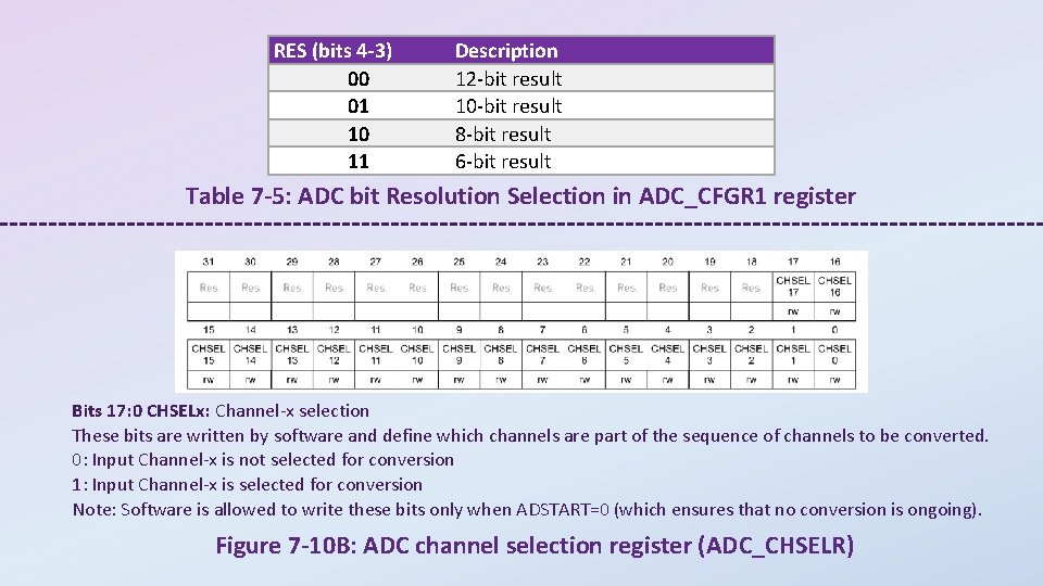
RES (bits 4 -3) 00 01 10 11 Description 12 -bit result 10 -bit result 8 -bit result 6 -bit result Table 7 -5: ADC bit Resolution Selection in ADC_CFGR 1 register Bits 17: 0 CHSELx: Channel-x selection These bits are written by software and define which channels are part of the sequence of channels to be converted. 0: Input Channel-x is not selected for conversion 1: Input Channel-x is selected for conversion Note: Software is allowed to write these bits only when ADSTART=0 (which ensures that no conversion is ongoing). Figure 7 -10 B: ADC channel selection register (ADC_CHSELR)
![Bit 4 0 Description ADC Channel Input Selection AWDCH4 0 0 x 00 0 Bit 4 -0 Description ADC Channel Input Selection AWDCH[4: 0] 0 x 00 0](https://slidetodoc.com/presentation_image_h2/a79a445fd022673d48d8e71d73aa3163/image-18.jpg)
Bit 4 -0 Description ADC Channel Input Selection AWDCH[4: 0] 0 x 00 0 x 01 0 x 02 0 x 03 0 x 04 0 x 05 0 x 06 0 x 07 0 x 08 0 x 09 0 x 0 A 0 x 0 B 0 x 0 C 0 x 0 D 0 x 0 E 0 x 0 F 0 x 10 0 x 11 Port PIN PA 0 PA 1 PA 2 PA 3 PA 4 PA 5 PA 6 PA 7 PB 0 PB 1 PC 0 PC 1 PC 2 PC 3 PC 4 PC 5 Temperature (internal) VREFINT (internal) Analog Input Channel ADC AIN 0 ADC AIN 1 ADC AIN 2 ADC AIN 3 ADC AIN 4 ADC AIN 5 ADC AIN 6 ADC AIN 7 ADC AIN 8 ADC AIN 9 ADC AIN 10 ADC AIN 11 ADC AIN 12 ADC AIN 13 ADC AIN 14 ADC AIN 15 ADC AIN 16 ADC AIN 17 Table 7 -6: ADC_CFGR 1 Register bits for ADC Channel Selection

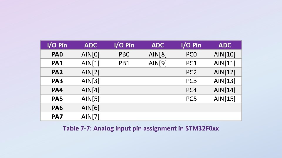
I/O Pin PA 0 PA 1 PA 2 PA 3 PA 4 PA 5 PA 6 PA 7 ADC AIN[0] AIN[1] AIN[2] AIN[3] AIN[4] AIN[5] AIN[6] AIN[7] I/O Pin PB 0 PB 1 ADC AIN[8] AIN[9] I/O Pin PC 0 PC 1 PC 2 PC 3 PC 4 PC 5 ADC AIN[10] AIN[11] AIN[12] AIN[13] AIN[14] AIN[15] Table 7 -7: Analog input pin assignment in STM 32 F 0 xx
![Bits 2 y 2 y1 MODERy1 0 Port x configuration bits y 0 Bits 2 y: 2 y+1 MODERy[1: 0]: Port x configuration bits (y = 0.](https://slidetodoc.com/presentation_image_h2/a79a445fd022673d48d8e71d73aa3163/image-20.jpg)
Bits 2 y: 2 y+1 MODERy[1: 0]: Port x configuration bits (y = 0. . 15) These bits are written by software to configure the I/O direction mode. 00: Input (reset state) 01: General purpose output mode 10: Alternate function mode 11: Analog mode Figure 7‑ 11: GPIO_MODER Register

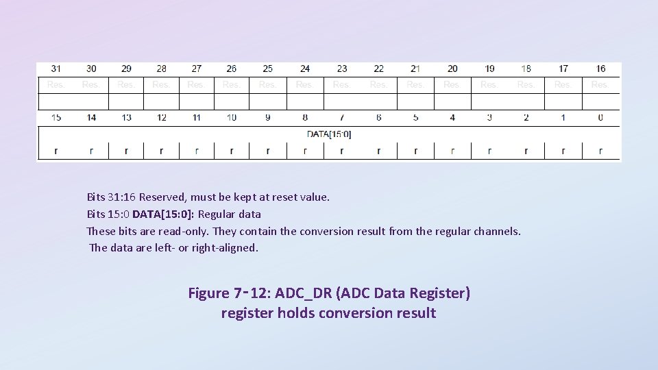
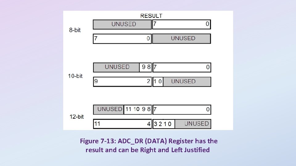
Bits 31: 16 Reserved, must be kept at reset value. Bits 15: 0 DATA[15: 0]: Regular data These bits are read-only. They contain the conversion result from the regular channels. The data are left- or right-aligned. Figure 7‑ 12: ADC_DR (ADC Data Register) register holds conversion result

Figure 7 -13: ADC_DR (DATA) Register has the result and can be Right and Left Justified

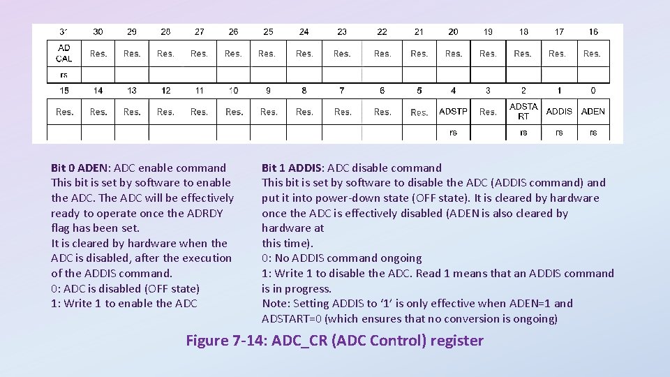
Bit 0 ADEN: ADC enable command This bit is set by software to enable the ADC. The ADC will be effectively ready to operate once the ADRDY flag has been set. It is cleared by hardware when the ADC is disabled, after the execution of the ADDIS command. 0: ADC is disabled (OFF state) 1: Write 1 to enable the ADC Bit 1 ADDIS: ADC disable command This bit is set by software to disable the ADC (ADDIS command) and put it into power-down state (OFF state). It is cleared by hardware once the ADC is effectively disabled (ADEN is also cleared by hardware at this time). 0: No ADDIS command ongoing 1: Write 1 to disable the ADC. Read 1 means that an ADDIS command is in progress. Note: Setting ADDIS to ‘ 1’ is only effective when ADEN=1 and ADSTART=0 (which ensures that no conversion is ongoing) Figure 7 -14: ADC_CR (ADC Control) register

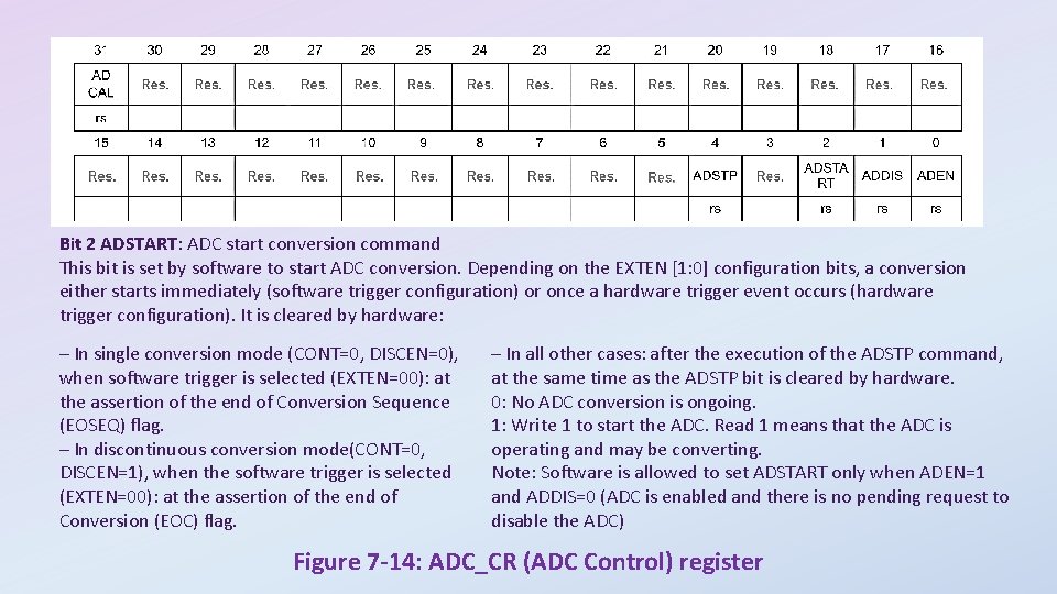
Bit 2 ADSTART: ADC start conversion command This bit is set by software to start ADC conversion. Depending on the EXTEN [1: 0] configuration bits, a conversion either starts immediately (software trigger configuration) or once a hardware trigger event occurs (hardware trigger configuration). It is cleared by hardware: – In single conversion mode (CONT=0, DISCEN=0), when software trigger is selected (EXTEN=00): at the assertion of the end of Conversion Sequence (EOSEQ) flag. – In discontinuous conversion mode(CONT=0, DISCEN=1), when the software trigger is selected (EXTEN=00): at the assertion of the end of Conversion (EOC) flag. – In all other cases: after the execution of the ADSTP command, at the same time as the ADSTP bit is cleared by hardware. 0: No ADC conversion is ongoing. 1: Write 1 to start the ADC. Read 1 means that the ADC is operating and may be converting. Note: Software is allowed to set ADSTART only when ADEN=1 and ADDIS=0 (ADC is enabled and there is no pending request to disable the ADC) Figure 7 -14: ADC_CR (ADC Control) register

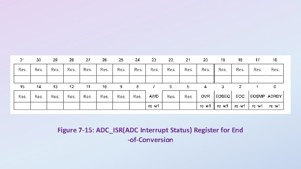
Figure 7 -15: ADC_ISR(ADC Interrupt Status) Register for End -of-Conversion

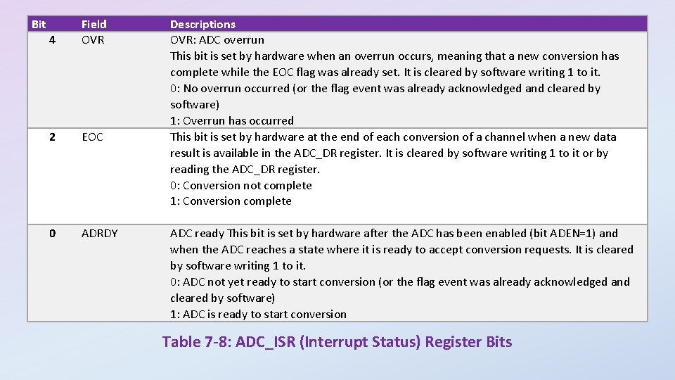
Bit 4 Field OVR 2 EOC 0 ADRDY Descriptions OVR: ADC overrun This bit is set by hardware when an overrun occurs, meaning that a new conversion has complete while the EOC flag was already set. It is cleared by software writing 1 to it. 0: No overrun occurred (or the flag event was already acknowledged and cleared by software) 1: Overrun has occurred This bit is set by hardware at the end of each conversion of a channel when a new data result is available in the ADC_DR register. It is cleared by software writing 1 to it or by reading the ADC_DR register. 0: Conversion not complete 1: Conversion complete ADC ready This bit is set by hardware after the ADC has been enabled (bit ADEN=1) and when the ADC reaches a state where it is ready to accept conversion requests. It is cleared by software writing 1 to it. 0: ADC not yet ready to start conversion (or the flag event was already acknowledged and cleared by software) 1: ADC is ready to start conversion Table 7 -8: ADC_ISR (Interrupt Status) Register Bits

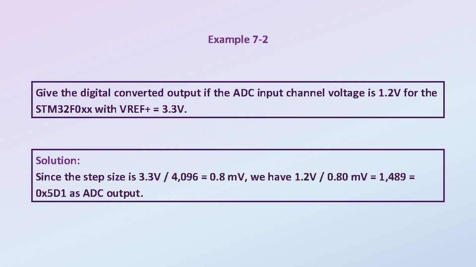
Example 7 -2 Give the digital converted output if the ADC input channel voltage is 1. 2 V for the STM 32 F 0 xx with VREF+ = 3. 3 V. Solution: Since the step size is 3. 3 V / 4, 096 = 0. 8 m. V, we have 1. 2 V / 0. 80 m. V = 1, 489 = 0 x 5 D 1 as ADC output.

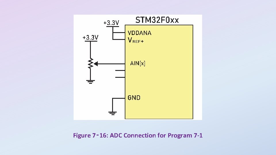
Figure 7‑ 16: ADC Connection for Program 7 -1

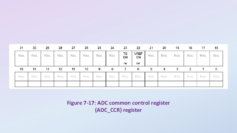
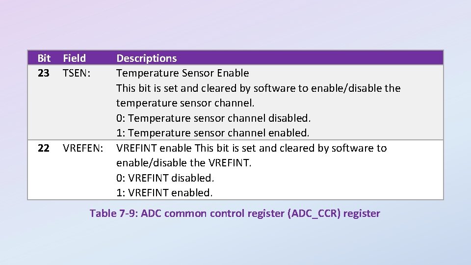
Figure 7 -17: ADC common control register (ADC_CCR) register

Bit 23 Field TSEN: 22 VREFEN: Descriptions Temperature Sensor Enable This bit is set and cleared by software to enable/disable the temperature sensor channel. 0: Temperature sensor channel disabled. 1: Temperature sensor channel enabled. VREFINT enable This bit is set and cleared by software to enable/disable the VREFINT. 0: VREFINT disabled. 1: VREFINT enabled. Table 7 -9: ADC common control register (ADC_CCR) register

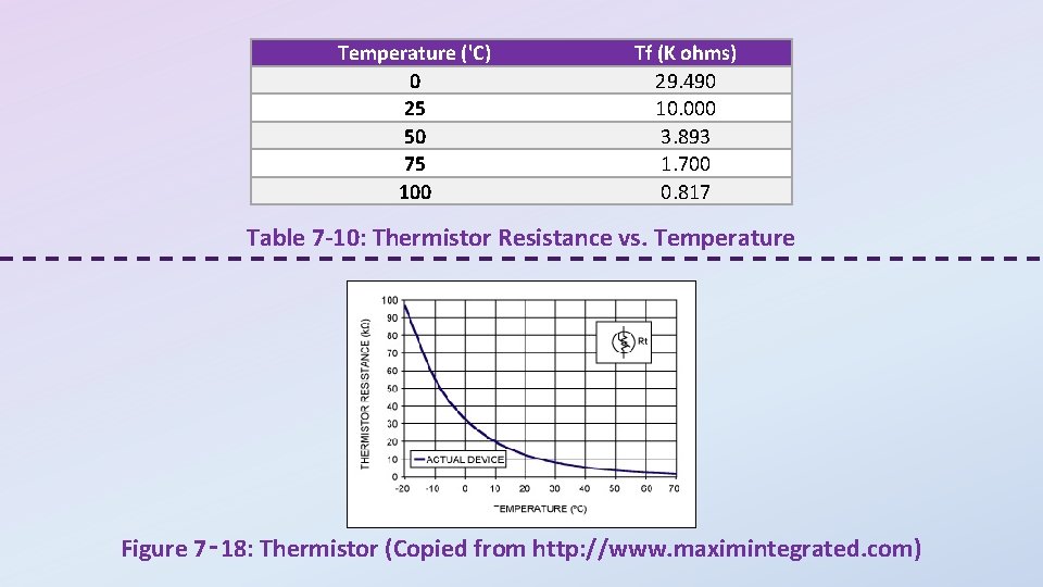
Temperature ('C) 0 25 50 75 100 Tf (K ohms) 29. 490 10. 000 3. 893 1. 700 0. 817 Table 7 -10: Thermistor Resistance vs. Temperature Figure 7‑ 18: Thermistor (Copied from http: //www. maximintegrated. com)

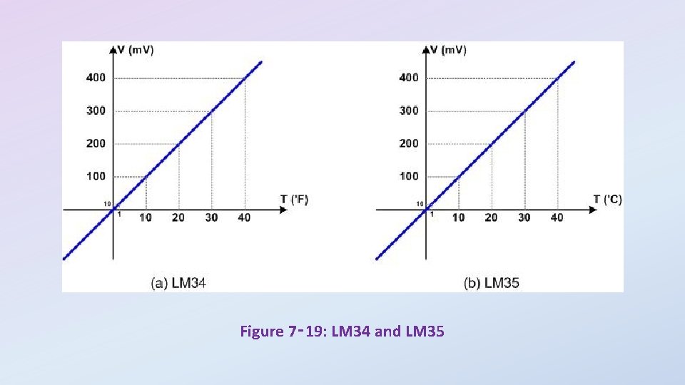
Figure 7‑ 19: LM 34 and LM 35

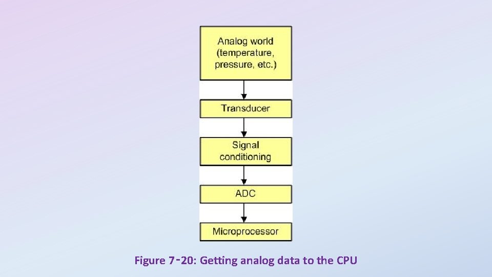
Figure 7‑ 20: Getting analog data to the CPU

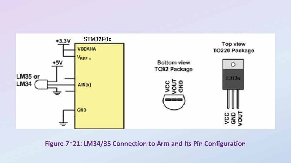
Figure 7‑ 21: LM 34/35 Connection to Arm and Its Pin Configuration

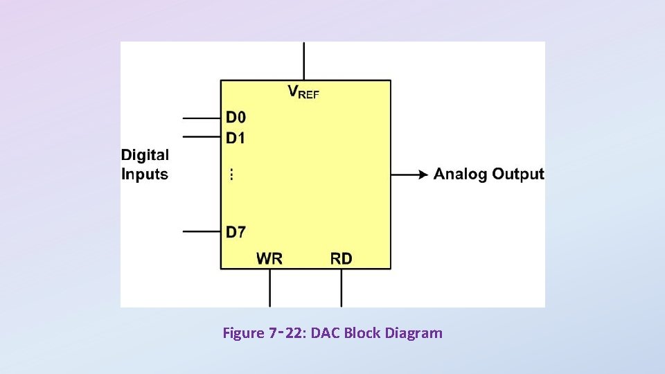
Figure 7‑ 22: DAC Block Diagram

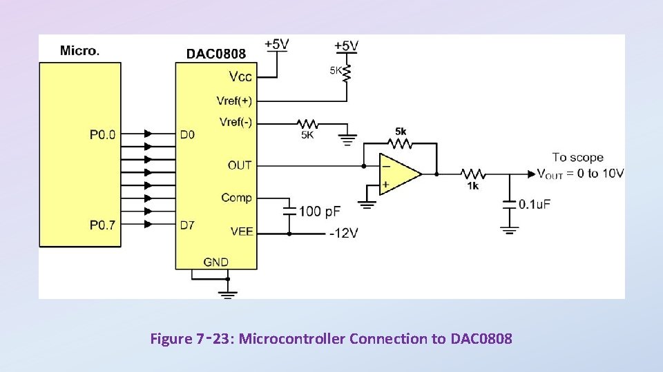
Figure 7‑ 23: Microcontroller Connection to DAC 0808

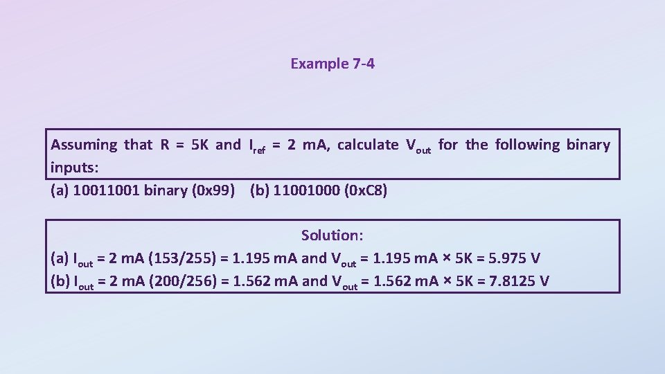
Example 7 -4 Assuming that R = 5 K and Iref = 2 m. A, calculate Vout for the following binary inputs: (a) 1001 binary (0 x 99) (b) 11001000 (0 x. C 8) Solution: (a) Iout = 2 m. A (153/255) = 1. 195 m. A and Vout = 1. 195 m. A × 5 K = 5. 975 V (b) Iout = 2 m. A (200/256) = 1. 562 m. A and Vout = 1. 562 m. A × 5 K = 7. 8125 V