Chapter 7 ADC DAC and Sensor Interfacing 1

- Slides: 49

Chapter 7 ADC, DAC, and Sensor Interfacing 1

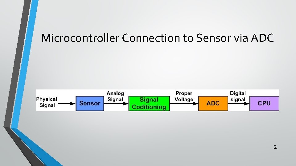
Microcontroller Connection to Sensor via ADC 2

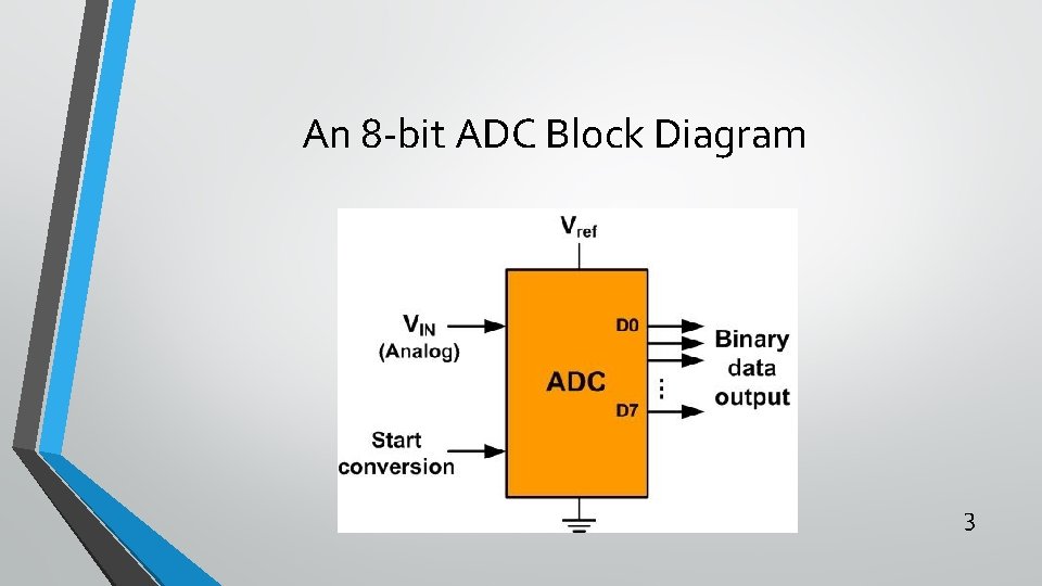
An 8 -bit ADC Block Diagram 3

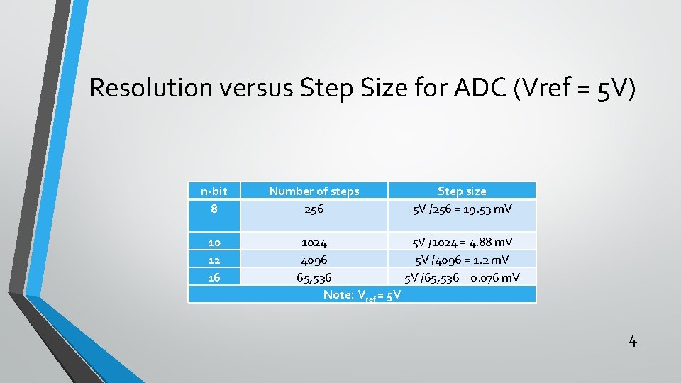
Resolution versus Step Size for ADC (Vref = 5 V) n-bit 8 10 12 16 Number of steps 256 Step size 5 V /256 = 19. 53 m. V 1024 5 V /1024 = 4. 88 m. V 4096 5 V /4096 = 1. 2 m. V 65, 536 5 V /65, 536 = 0. 076 m. V Note: Vref = 5 V 4

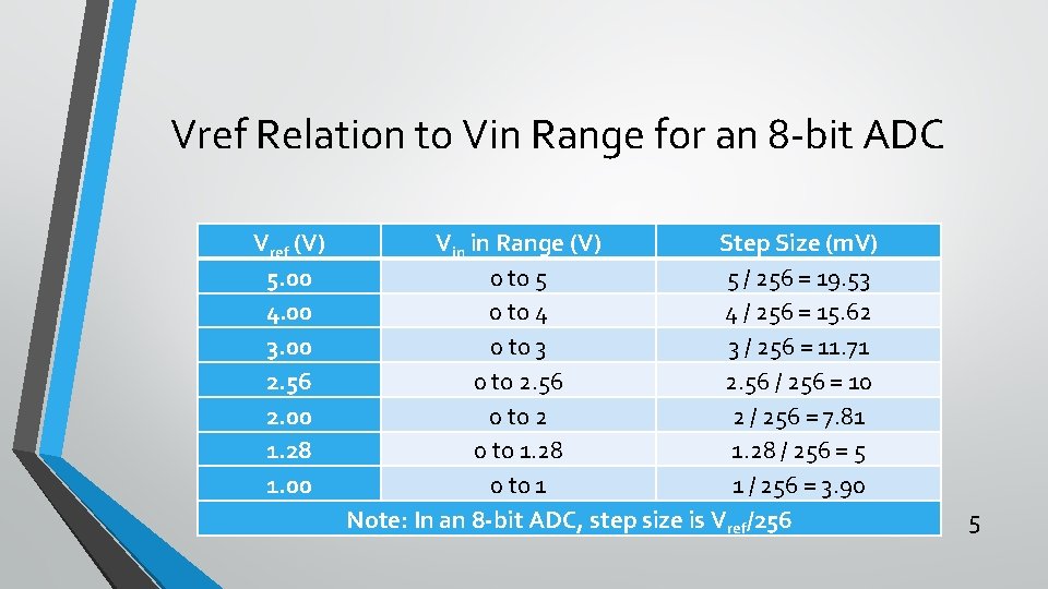
Vref Relation to Vin Range for an 8 -bit ADC Vref (V) 5. 00 4. 00 3. 00 2. 56 2. 00 1. 28 1. 00 Vin in Range (V) Step Size (m. V) 0 to 5 5 / 256 = 19. 53 0 to 4 4 / 256 = 15. 62 0 to 3 3 / 256 = 11. 71 0 to 2. 56 / 256 = 10 0 to 2 2 / 256 = 7. 81 0 to 1. 28 / 256 = 5 0 to 1 1 / 256 = 3. 90 Note: In an 8 -bit ADC, step size is Vref/256 5

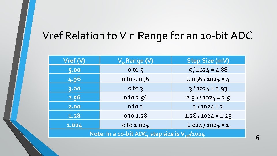
Vref Relation to Vin Range for an 10 -bit ADC Vref (V) 5. 00 4. 96 3. 00 2. 56 2. 00 1. 28 1. 024 Vin. Range (V) Step Size (m. V) 0 to 5 5 / 1024 = 4. 88 0 to 4. 096 / 1024 = 4 0 to 3 3 / 1024 = 2. 93 0 to 2. 56 / 1024 = 2. 5 0 to 2 2 / 1024 = 2 0 to 1. 28 / 1024 = 1. 25 0 to 1. 024 / 1024 = 1 Note: In a 10 -bit ADC, step size is Vref/1024 6

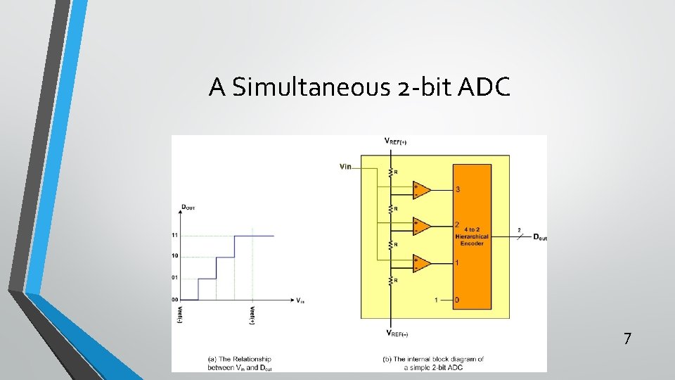
A Simultaneous 2 -bit ADC 7

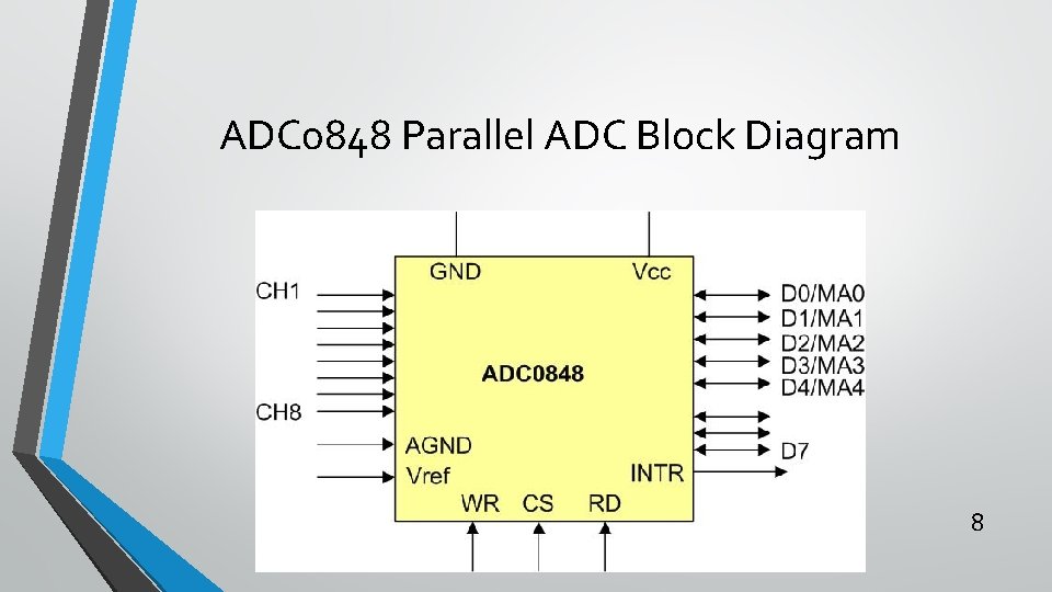
ADC 0848 Parallel ADC Block Diagram 8

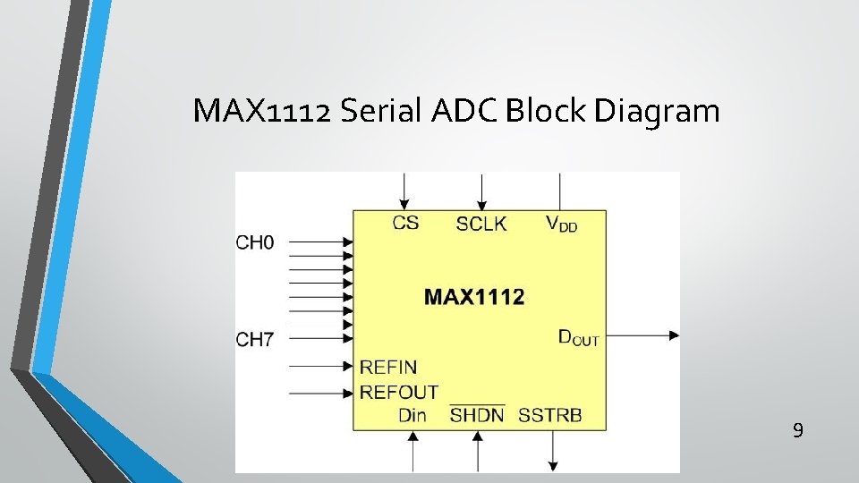
MAX 1112 Serial ADC Block Diagram 9

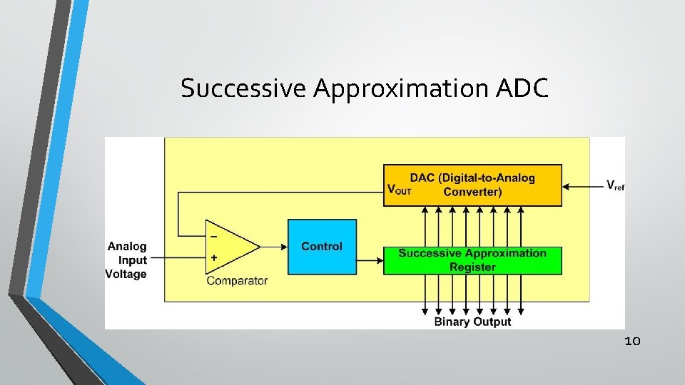
Successive Approximation ADC 10

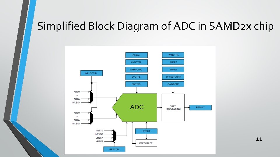
Simplified Block Diagram of ADC in SAMD 2 x chip 11

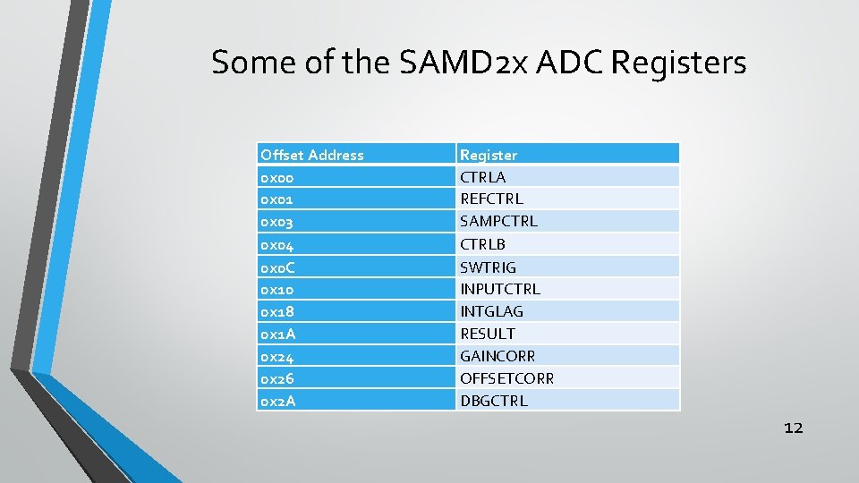
Some of the SAMD 2 x ADC Registers Offset Address 0 x 00 0 x 01 0 x 03 0 x 04 0 x 0 C 0 x 10 0 x 18 0 x 1 A 0 x 24 0 x 26 0 x 2 A Register CTRLA REFCTRL SAMPCTRLB SWTRIG INPUTCTRL INTGLAG RESULT GAINCORR OFFSETCORR DBGCTRL 12

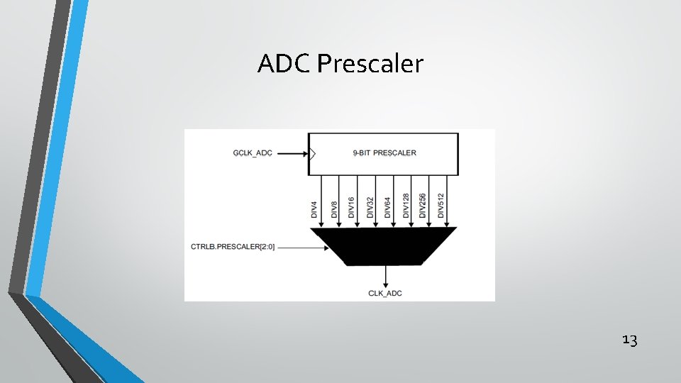
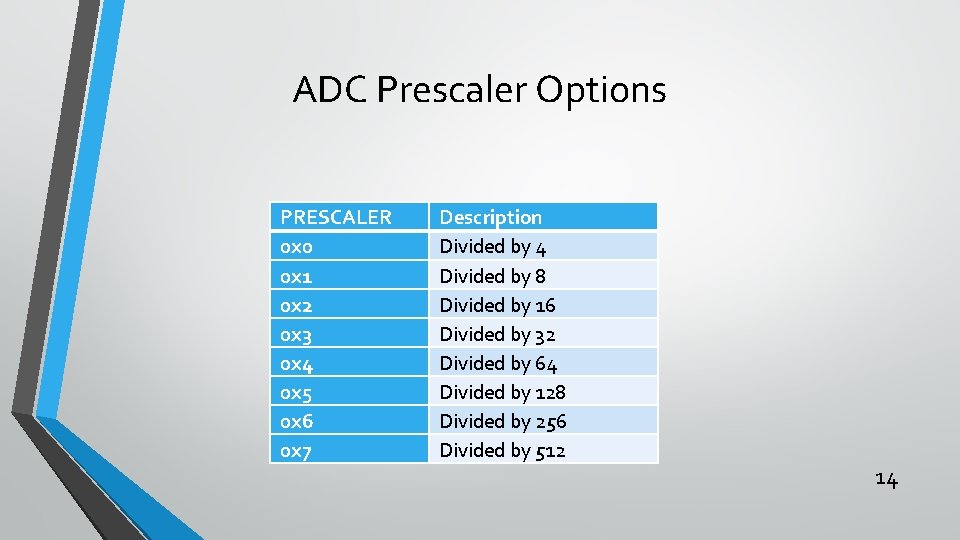
ADC Prescaler 13

ADC Prescaler Options PRESCALER 0 x 0 0 x 1 0 x 2 0 x 3 0 x 4 0 x 5 0 x 6 0 x 7 Description Divided by 4 Divided by 8 Divided by 16 Divided by 32 Divided by 64 Divided by 128 Divided by 256 Divided by 512 14

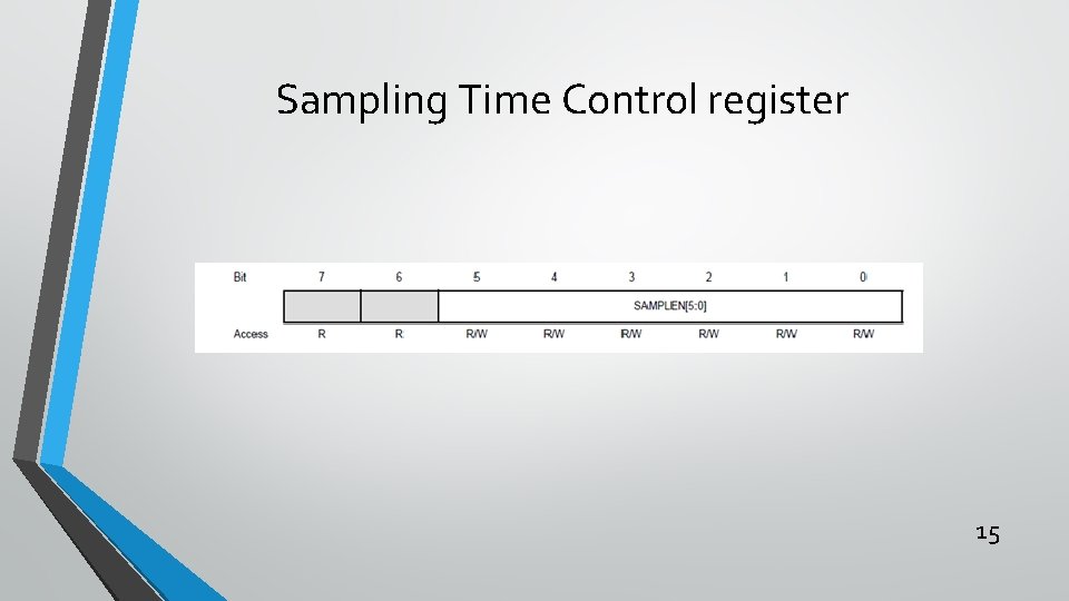
Sampling Time Control register 15

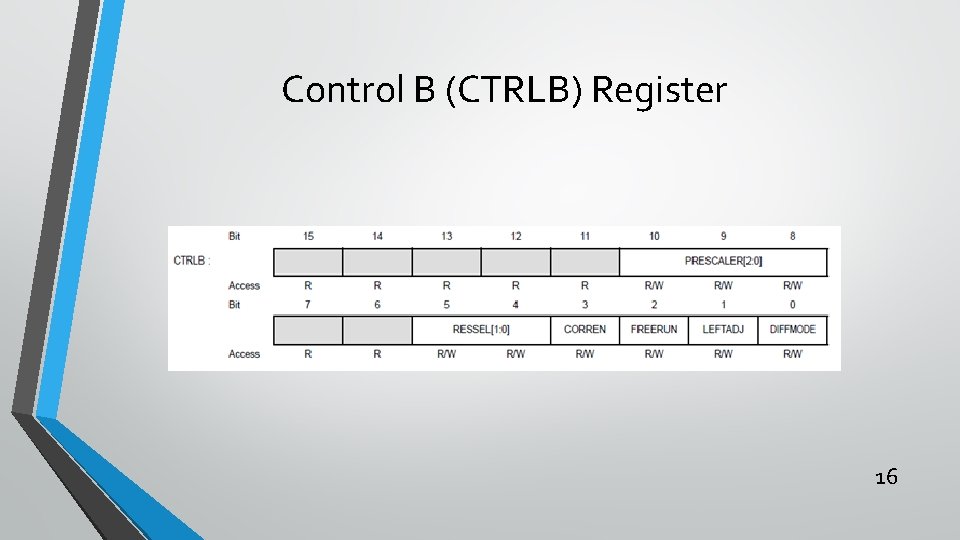
Control B (CTRLB) Register 16

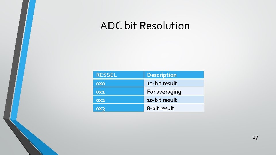
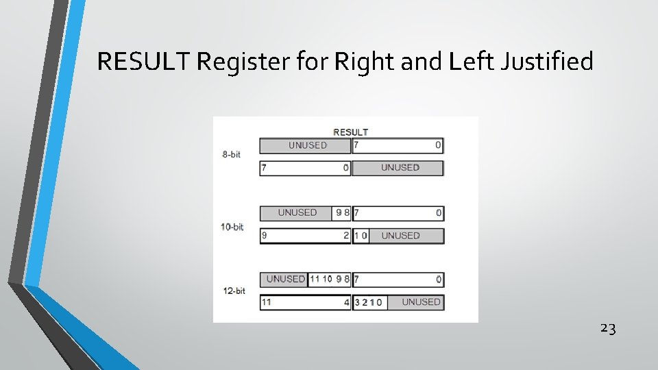
ADC bit Resolution RESSEL 0 x 0 0 x 1 0 x 2 0 x 3 Description 12 -bit result For averaging 10 -bit result 8 -bit result 17

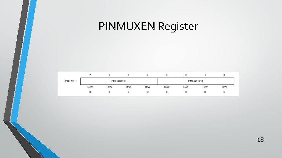
PINMUXEN Register 18

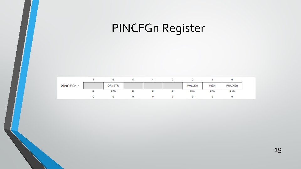
PINCFGn Register 19

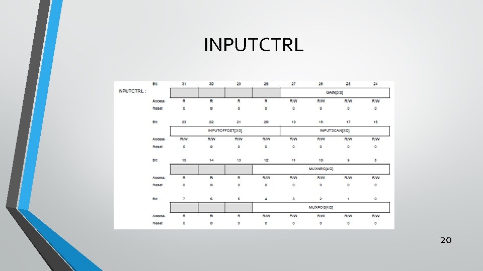
INPUTCTRL 20

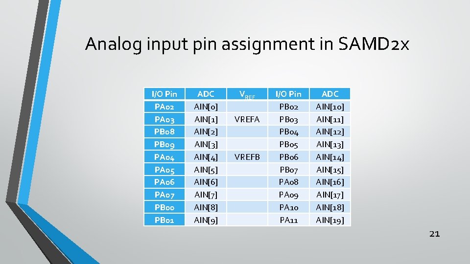
Analog input pin assignment in SAMD 2 x I/O Pin PA 02 PA 03 PB 08 PB 09 PA 04 PA 05 PA 06 PA 07 PB 00 PB 01 ADC AIN[0] AIN[1] AIN[2] AIN[3] AIN[4] AIN[5] AIN[6] AIN[7] AIN[8] AIN[9] VREFA VREFB I/O Pin PB 02 PB 03 PB 04 PB 05 PB 06 PB 07 PA 08 PA 09 PA 10 PA 11 ADC AIN[10] AIN[11] AIN[12] AIN[13] AIN[14] AIN[15] AIN[16] AIN[17] AIN[18] AIN[19] 21

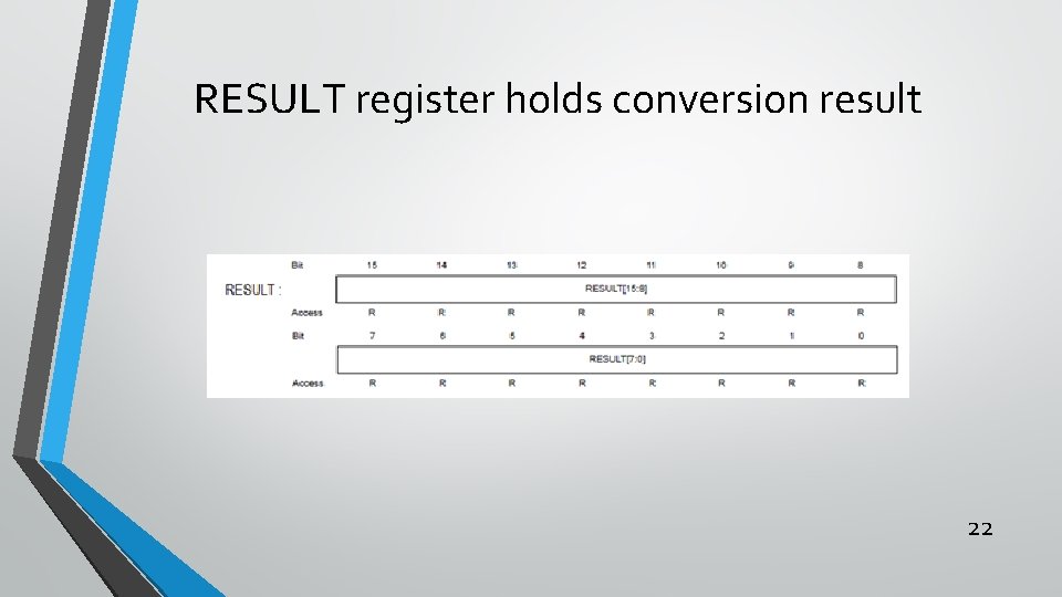
RESULT register holds conversion result 22

RESULT Register for Right and Left Justified 23

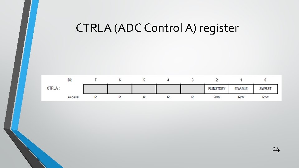
CTRLA (ADC Control A) register 24

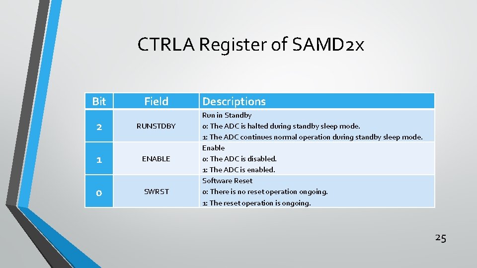
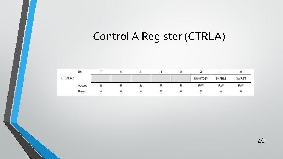
CTRLA Register of SAMD 2 x Bit Field 2 RUNSTDBY 1 ENABLE 0 SWRST Descriptions Run in Standby 0: The ADC is halted during standby sleep mode. 1: The ADC continues normal operation during standby sleep mode. Enable 0: The ADC is disabled. 1: The ADC is enabled. Software Reset 0: There is no reset operation ongoing. 1: The reset operation is ongoing. 25

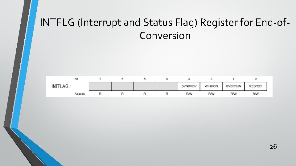
INTFLG (Interrupt and Status Flag) Register for End-of. Conversion 26

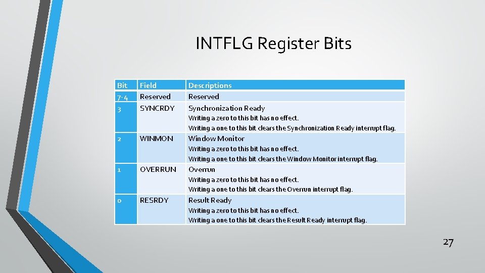
INTFLG Register Bits Bit 7 -4 3 Field Reserved SYNCRDY Descriptions Reserved Synchronization Ready Writing a zero to this bit has no effect. Writing a one to this bit clears the Synchronization Ready interrupt flag. 2 WINMON Window Monitor Writing a zero to this bit has no effect. Writing a one to this bit clears the Window Monitor interrupt flag. 1 OVERRUN Overrun Writing a zero to this bit has no effect. Writing a one to this bit clears the Overrun interrupt flag. 0 RESRDY Result Ready Writing a zero to this bit has no effect. Writing a one to this bit clears the Result Ready interrupt flag. 27

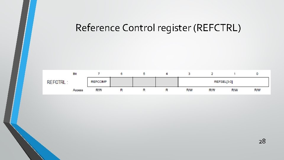
Reference Control register (REFCTRL) 28

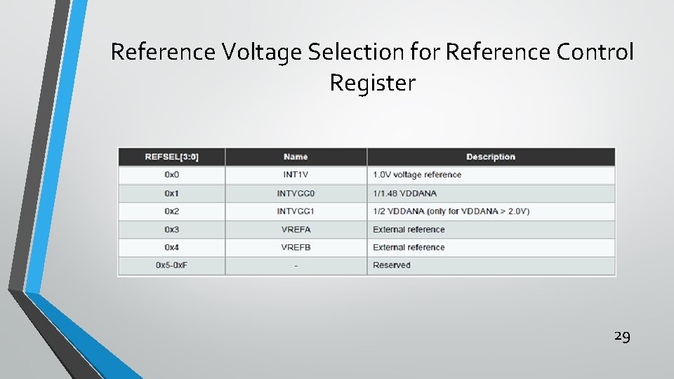
Reference Voltage Selection for Reference Control Register 29

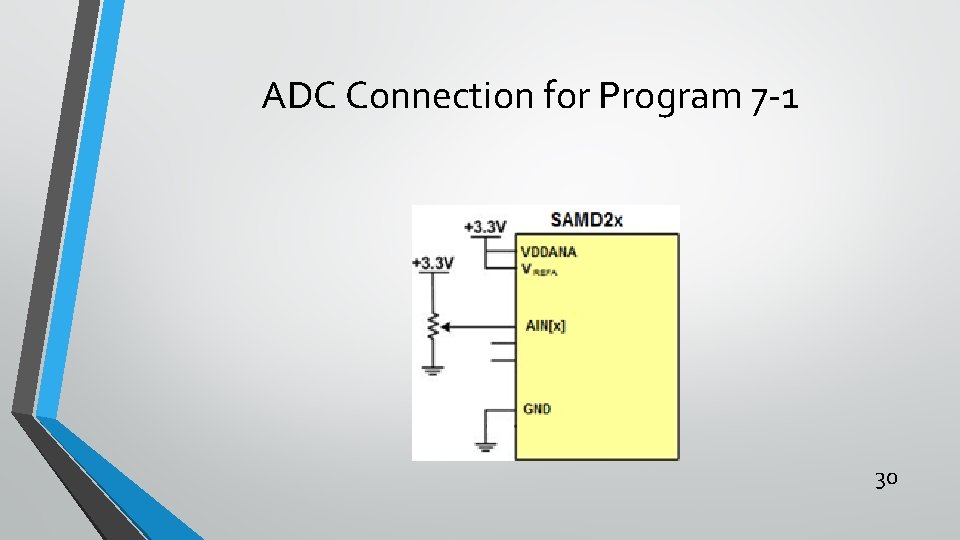
ADC Connection for Program 7 -1 30

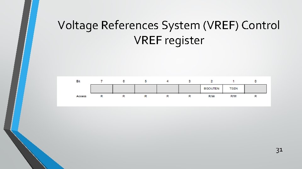
Voltage References System (VREF) Control VREF register 31

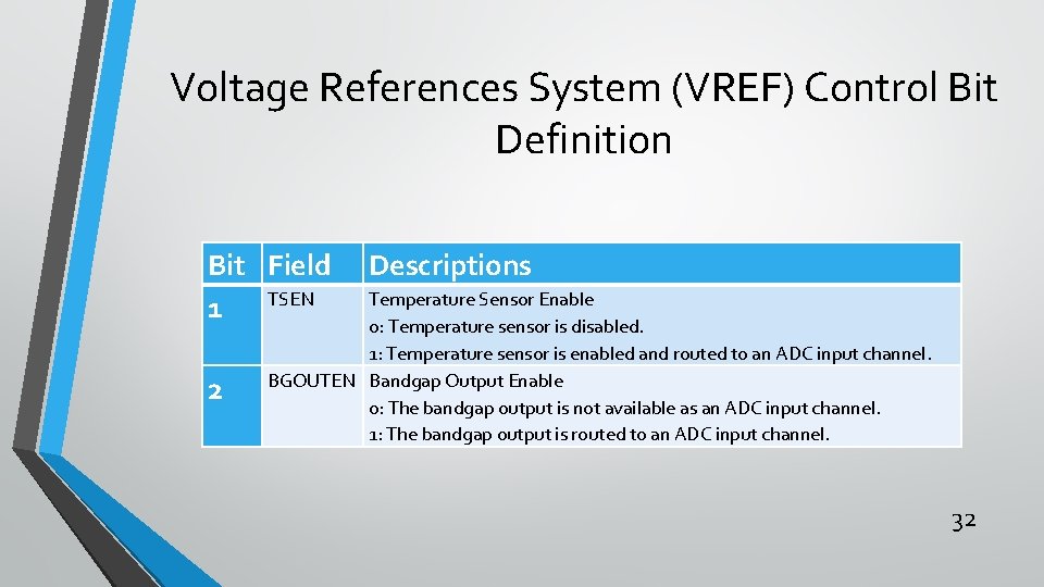
Voltage References System (VREF) Control Bit Definition Bit Field 1 TSEN 2 Descriptions Temperature Sensor Enable 0: Temperature sensor is disabled. 1: Temperature sensor is enabled and routed to an ADC input channel. BGOUTEN Bandgap Output Enable 0: The bandgap output is not available as an ADC input channel. 1: The bandgap output is routed to an ADC input channel. 32

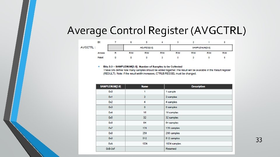
Average Control Register (AVGCTRL) 33

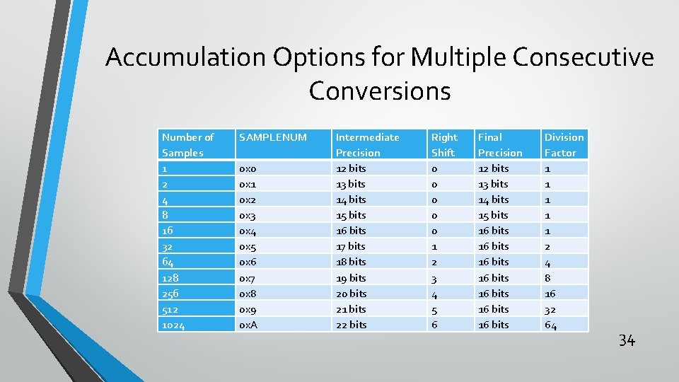
Accumulation Options for Multiple Consecutive Conversions Number of Samples 1 2 4 8 16 32 64 128 256 512 1024 SAMPLENUM 0 x 0 0 x 1 0 x 2 0 x 3 0 x 4 0 x 5 0 x 6 0 x 7 0 x 8 0 x 9 0 x. A Intermediate Precision 12 bits 13 bits 14 bits 15 bits 16 bits 17 bits 18 bits 19 bits 20 bits 21 bits 22 bits Right Shift 0 0 0 1 2 3 4 5 6 Final Precision 12 bits 13 bits 14 bits 15 bits 16 bits 16 bits Division Factor 1 1 1 2 4 8 16 32 64 34

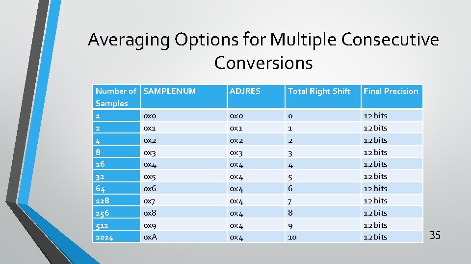
Averaging Options for Multiple Consecutive Conversions Number of Samples 1 2 4 8 16 32 64 128 256 512 1024 SAMPLENUM ADJRES Total Right Shift Final Precision 0 x 0 0 x 1 0 x 2 0 x 3 0 x 4 0 x 5 0 x 6 0 x 7 0 x 8 0 x 9 0 x. A 0 x 0 0 x 1 0 x 2 0 x 3 0 x 4 0 x 4 0 1 2 3 4 5 6 7 8 9 10 12 bits 12 bits 12 bits 35

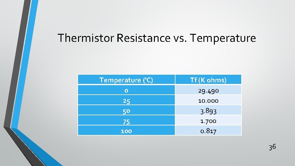
Thermistor Resistance vs. Temperature ('C) 0 25 50 75 100 Tf (K ohms) 29. 490 10. 000 3. 893 1. 700 0. 817 36

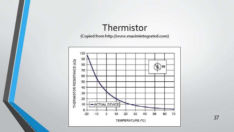
Thermistor (Copied from http: //www. maximintegrated. com) 37

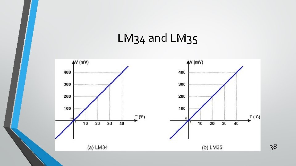
LM 34 and LM 35 38

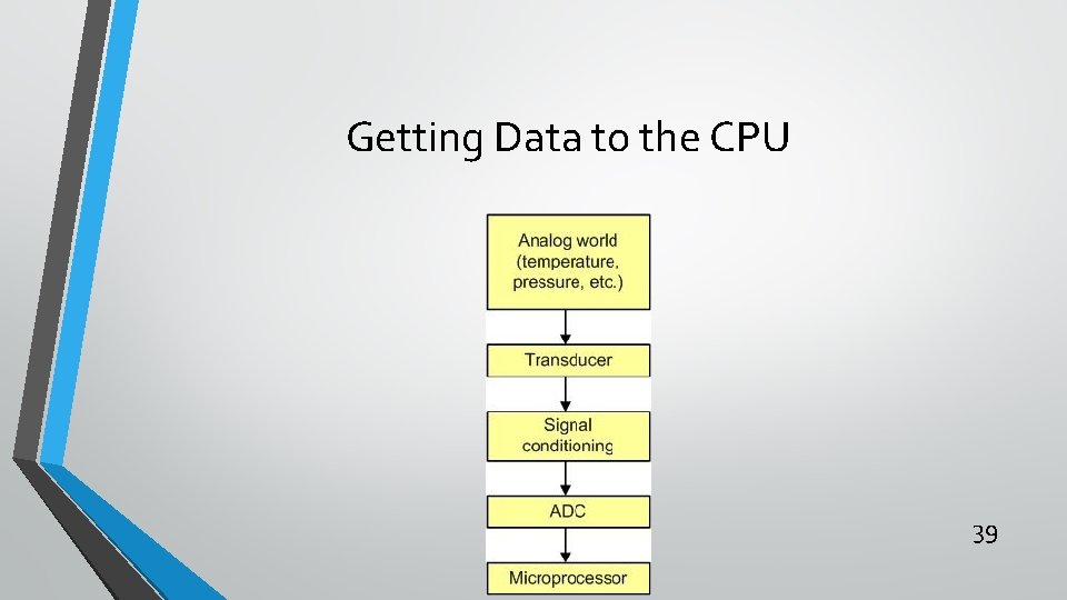
Getting Data to the CPU 39

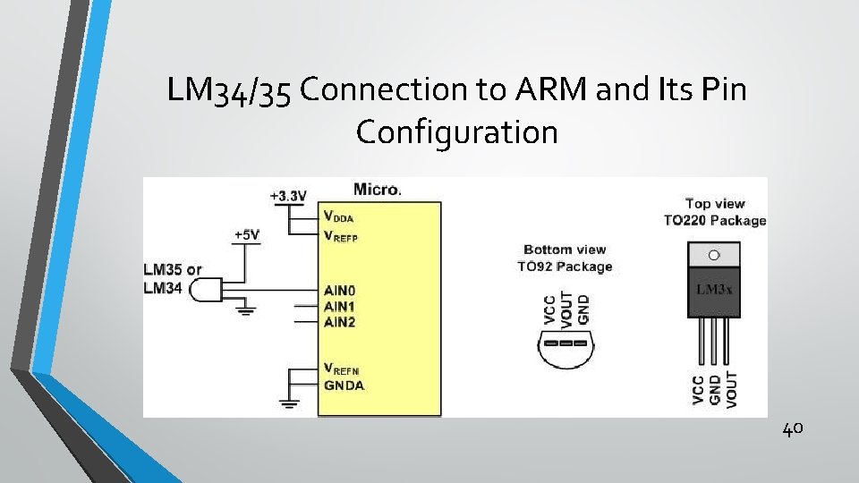
LM 34/35 Connection to ARM and Its Pin Configuration 40

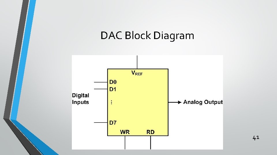
DAC Block Diagram 41

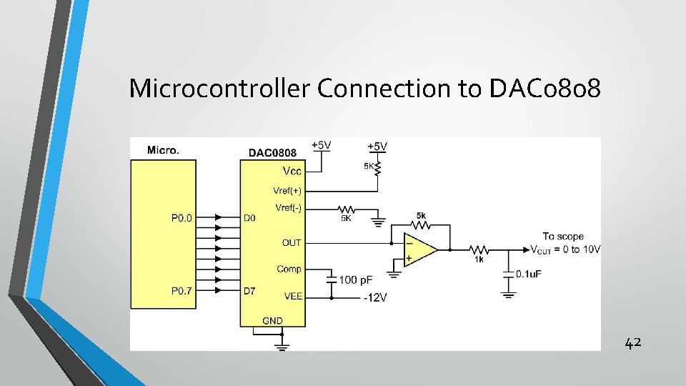
Microcontroller Connection to DAC 0808 42

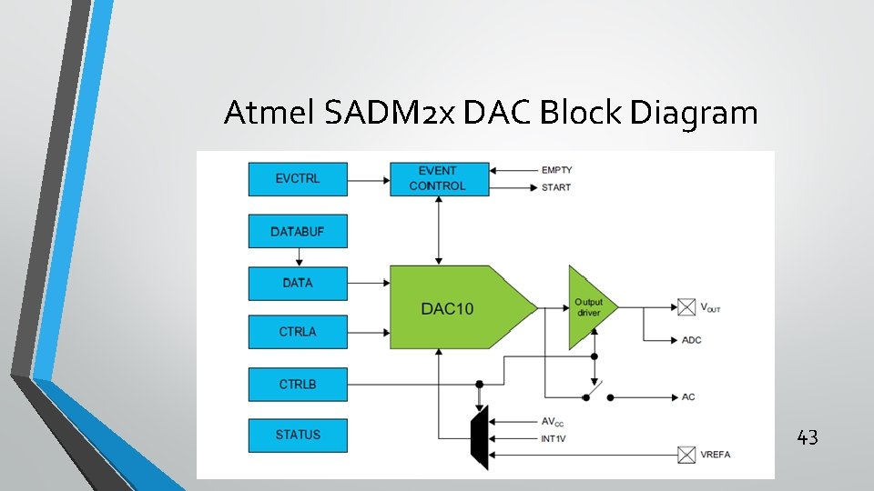
Atmel SADM 2 x DAC Block Diagram 43

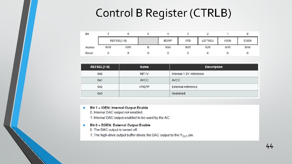
Control B Register (CTRLB) 44

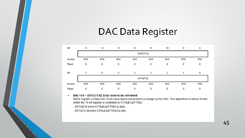
DAC Data Register 45

Control A Register (CTRLA) 46

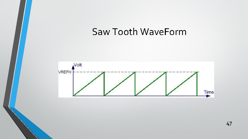
Saw Tooth Wave. Form 47

Angle vs. Voltage Magnitude for Sine Wave 48

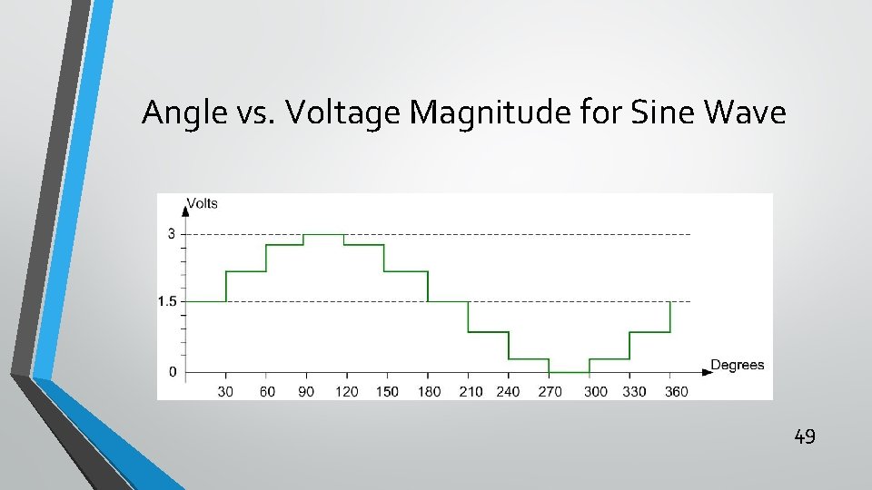
Angle vs. Voltage Magnitude for Sine Wave 49