Chapter 4 Interfacing IO Devices Microprocessors Interfacing 1
- Slides: 20

Chapter 4 Interfacing I/O Devices Microprocessors & Interfacing 1

Interfacing I/O Devices • • • Using I/O devices data can be transferred between the microprocessor and the outside world. This can be done in groups of 8 bits using the entire data bus. This is called parallel I/O. The other method is serial I/O where one bit is transferred at a time using the SI and SO pins on the Microprocessors & Interfacing 2

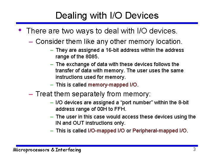
Dealing with I/O Devices • There are two ways to deal with I/O devices. – Consider them like any other memory location. – They are assigned a 16 -bit address within the address range of the 8085. – The exchange of data with these devices follows the transfer of data with memory. The user uses the same instructions used for memory. – This is called memory-mapped I/O. – Treat them separately from memory: – I/O devices are assigned a “port number” within the 8 -bit address range of 00 H to FFH. – The user in this case would access these devices using the IN and OUT instructions only. – This is called I/O-mapped I/O or Peripheral-mapped I/O. Microprocessors & Interfacing 3

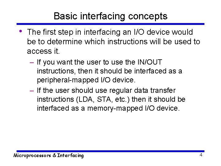
Basic interfacing concepts • The first step in interfacing an I/O device would be to determine which instructions will be used to access it. – If you want the user to use the IN/OUT instructions, then it should be interfaced as a peripheral-mapped I/O device. – If the user should use regular data transfer instructions (LDA, STA, etc. ) then it should be interfaced as a memory-mapped I/O device. Microprocessors & Interfacing 4

Peripheral I/O instructions • There are two instructions: – IN brings data (8 -bits) from an input device to the accumulator – OUT brings data (8 -bits) from the accumulator to an output device. – They are both 2 byte instructions with the second byte holding the 8 -bit address of the device. • Note: Given that there are separate instructions for input and output, the 8085 can actually communicate with 256 different input devices AND an additional 256 different output devices. Microprocessors & Interfacing 5

The execution of the OUT instruction • The OUT instruction requires 3 machine cycles and 10 T-states. – The first cycle is an opcode fetch cycle to fetch the 1 st byte of the instruction from memory (OUT). – The second cycle is a memory read cycle to bring the 8 -bit port number from the next location. – The third cycle is an I/O write cycle. • In this cycle, the 8085 places the port number on AD 0 AD 7 AND A 8 -A 15 and the signal WR is set low (active). – Since the device address is placed on both AD 0 -AD 7 as well as A 8 -A 15, there is no need for de-multiplexing AD 0 AD 7. A 8 -A 15 can be used directly to identify the device. Microprocessors & Interfacing 6

The execution of the IN instruction • The execution of the IN instruction is almost identical to that of the OUT instruction. 3 machine cycles, 10 T-states. – The first machine cycle is the opcode fetch. – The second cycle is the memory read to get the port number. – The third is an I/O Read cycle. • Again, in T 1 the port address (8 -bits) is placed on both AD 0 - AD 7, and A 8 -A 15. The IO/M signal is set high to indicate an I/O operation. At the beginning of T 2, the RD signal is set low (active) and the I/O device responds by placing the 8 -bit data on the data bus. Microprocessors & Interfacing 7

The interfacing of output devices – Output devices are usually slow. – Also, the output is usually expected to continue appearing on the output device for a long period of time. – Given that the data will only be present on the data lines for a very short period (microseconds), it has to be latched externally. • To do this the external latch should be enabled when the port’s address is present on the address bus, the IO/M signal is set high and WR is set low. – The resulting signal would be active when the output device is being accessed by the microprocessor. – Decoding the address bus (for memory-mapped devices) follows the same techniques discussed in interfacing memory. Microprocessors & Interfacing 8

Interfacing of input devices • The basic concepts are similar to interfacing of output devices. • The address lines are decoded to generate a signal that is active when the particular port is being accessed. • An IORD signal is generated by combining the IO/M and the RD signals from the microprocessor. • A tri-state buffer is used to connect the input device to the data bus. The control (Enable) for these buffers is connected to the result of combining the address signal and the signal IORD. Microprocessors & Interfacing 9

Examples of Interfacing I/O Devices • To illustrate the techniques of interfacing I/O devices we will design the circuits needed to interface 8 LEDs to display the contents of the accumulator as well as 8 switches to set the contents of the accumulator. Microprocessors & Interfacing 10

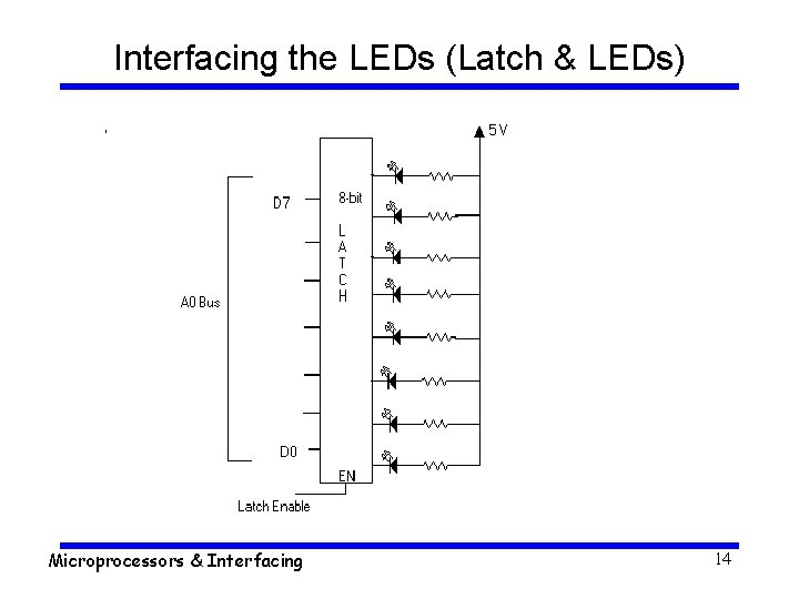
Interfacing the LEDs • Let’s first design the external circuit. – The data on the data bus from the microprocessor stays for an extremely short amount of time. So, in order to keep it long enough for displaying, we will need an external latch. • We will use an 8 -bit latch to hold the data we need to connect the 8 LED to the latches outputs. – However, the latch will not be able to source enough current. So, we will use the inverted outputs and make it sink the current instead. Microprocessors & Interfacing 11

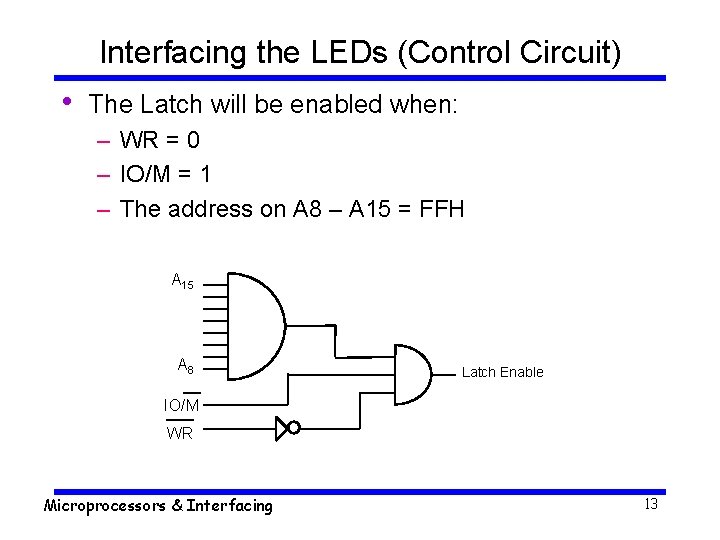
When should the latch be enabled? • It needs to be enabled when the data is on the data bus. – That happens when the ALE signal is low. However, we only want to display the data that is being sent to the I/O, we don’t want to display the data being saved in memory. – So, the latch needs to be enabled only during I/O operations. That happens when IO/M=1 – Finally we only want to display data intended for our port. We must decide on a port number. • Let’s say FFH. • Now, we can design the control circuit. Microprocessors & Interfacing 12

Interfacing the LEDs (Control Circuit) • The Latch will be enabled when: – WR = 0 – IO/M = 1 – The address on A 8 – A 15 = FFH A 15 A 8 Latch Enable IO/M WR Microprocessors & Interfacing 13

Interfacing the LEDs (Latch & LEDs) Microprocessors & Interfacing 14

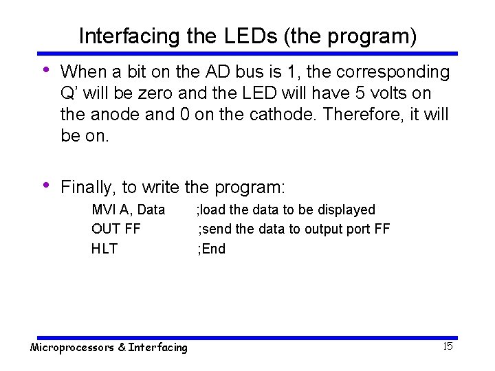
Interfacing the LEDs (the program) • When a bit on the AD bus is 1, the corresponding Q’ will be zero and the LED will have 5 volts on the anode and 0 on the cathode. Therefore, it will be on. • Finally, to write the program: MVI A, Data OUT FF HLT Microprocessors & Interfacing ; load the data to be displayed ; send the data to output port FF ; End 15

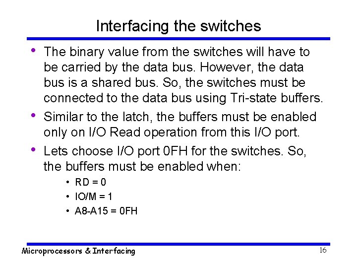
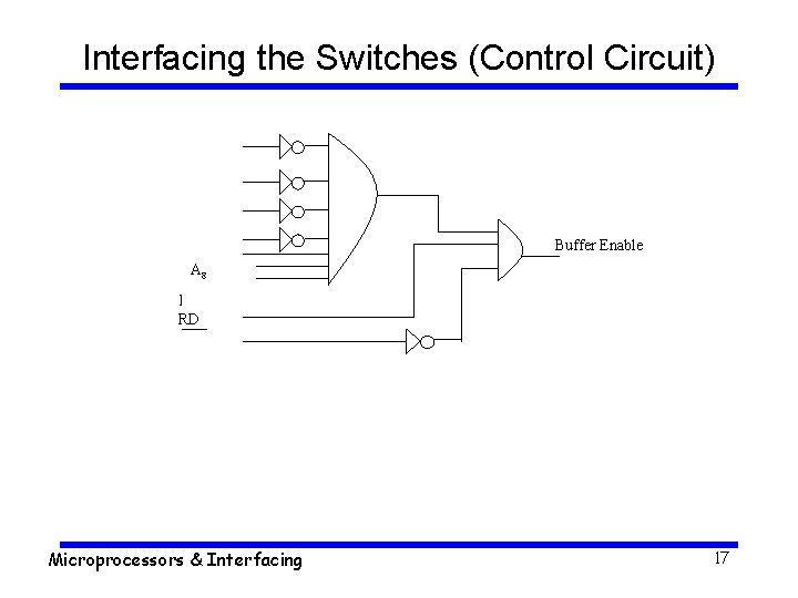
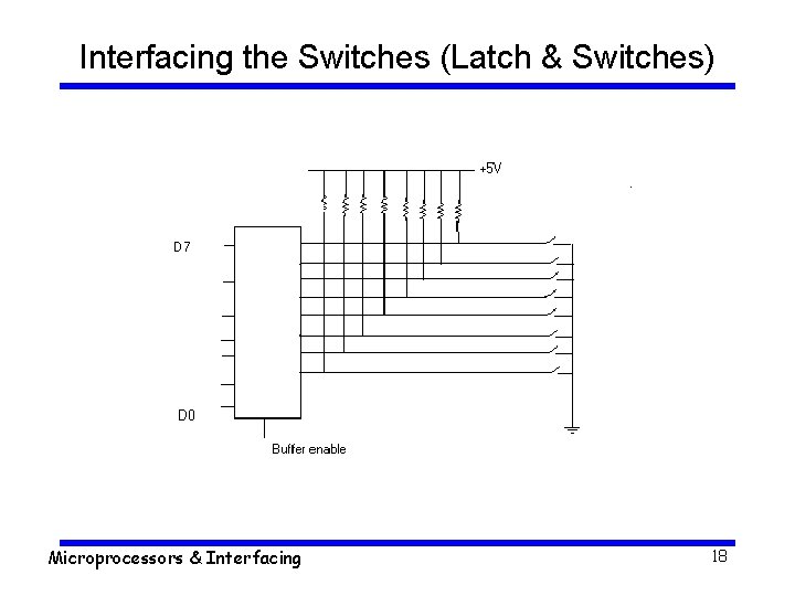
Interfacing the switches • • • The binary value from the switches will have to be carried by the data bus. However, the data bus is a shared bus. So, the switches must be connected to the data bus using Tri-state buffers. Similar to the latch, the buffers must be enabled only on I/O Read operation from this I/O port. Lets choose I/O port 0 FH for the switches. So, the buffers must be enabled when: • RD = 0 • IO/M = 1 • A 8 -A 15 = 0 FH Microprocessors & Interfacing 16

Interfacing the Switches (Control Circuit) Buffer Enable A 8 IO/M RD Microprocessors & Interfacing 17

Interfacing the Switches (Latch & Switches) Microprocessors & Interfacing 18

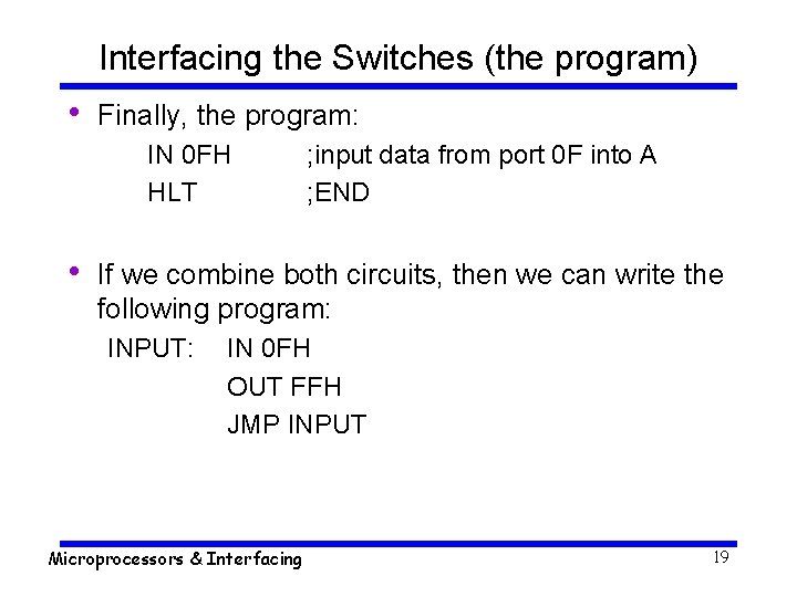
Interfacing the Switches (the program) • Finally, the program: IN 0 FH HLT • ; input data from port 0 F into A ; END If we combine both circuits, then we can write the following program: INPUT: IN 0 FH OUT FFH JMP INPUT Microprocessors & Interfacing 19

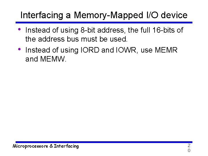
Interfacing a Memory-Mapped I/O device • • Instead of using 8 -bit address, the full 16 -bits of the address bus must be used. Instead of using IORD and IOWR, use MEMR and MEMW. Microprocessors & Interfacing 2 0