
CALYPSO HERCROMxx G 2 Albinzhangti com Texas Instruments
CALYPSO HERCROMxx. G 2 Albin-zhang@ti. com Texas Instruments Shanghai Wireless Customer Integration & Design Center 1
Calypso General Description * DO NOT COPY * 2
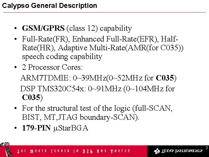
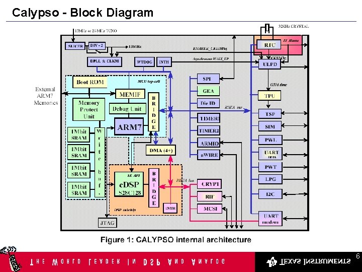
Calypso General Description • GSM/GPRS (class 12) capability • Full-Rate(FR), Enhanced Full-Rate(EFR), Half. Rate(HR), Adaptive Multi-Rate(AMR(for C 035)) speech coding capability • 2 Processor Cores: ARM 7 TDMIE: 0~39 MHz(0~52 MHz for C 035) DSP TMS 320 C 54 x: 0~91 MHz (0~104 MHz for C 035) • For the structural test of the logic (full-SCAN, BIST, MT, JTAG boundary-SCAN). • 179 -PIN m. Star. BGA 3
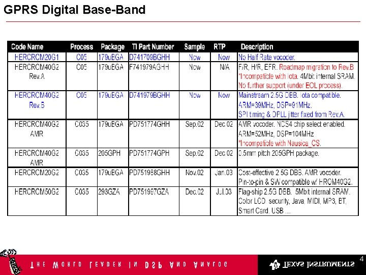
GPRS Digital Base-Band 4
CALYPSO - Overview CALYPSO OVERVIEW * DO NOT COPY * 5
Calypso - Block Diagram 6
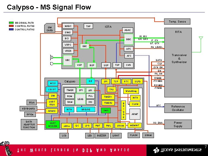
Calypso - MS Signal Flow BB SIGNAL PATH CONTROL PATHS Temp. Sense SIM CARD MADC TAP IOTA ADAC SIMS BCI RITA IR, IRX QR, QRX BBC VRPC IBIC PA_LEVEL APC VREG IT, ITX QT, QTX AFC DATA VBC VSP BSP TSP USP CLK CKG Transceiver & Synthesizer SYN_EN EN PA_ON MCSI Calypso CRYPT TIMER SIM RIF SPI ROM IRDA KEYBOARD ARMIO RAM PLL TIMER 1 XIO TIMER 2 BRIDGE INTH UART MODEM u. Wire LCD I 2 C LPG Watch. Dog INTH B R I D G E DMA LED PWT PWL BUZZER RX 900 /TX 1800 ULPD RX 1800 /TX 900 GPIOs DATA ADAPTOR FUNCTION RTC TPU API LEAD UART IRDA TSP SPI SRAM LIGHT CLKM AFC Reference Oscillator ARM 7 XO_ENA MEMINT FLASH Power Supply SRAM 7
Calypso - MEMINT Memory Interface 8
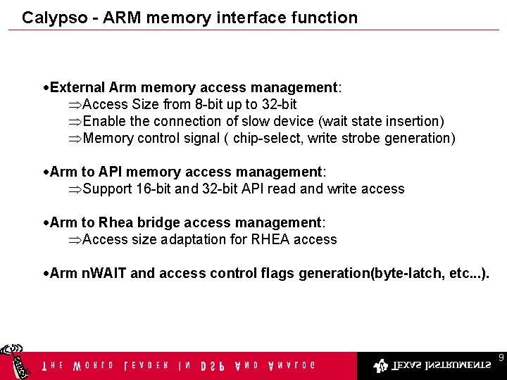
Calypso - ARM memory interface function ·External Arm memory access management: ÞAccess Size from 8 -bit up to 32 -bit ÞEnable the connection of slow device (wait state insertion) ÞMemory control signal ( chip-select, write strobe generation) ·Arm to API memory access management: ÞSupport 16 -bit and 32 -bit API read and write access ·Arm to Rhea bridge access management: ÞAccess size adaptation for RHEA access ·Arm n. WAIT and access control flags generation(byte-latch, etc. . . ). 9
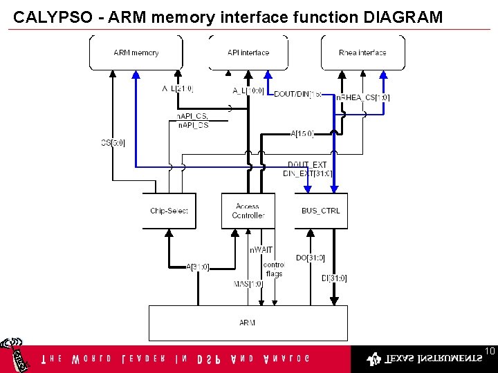
CALYPSO - ARM memory interface function DIAGRAM 10
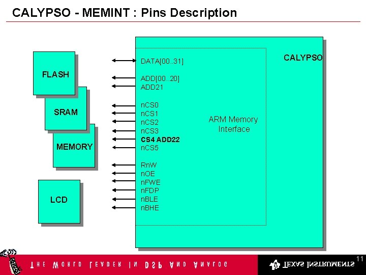
CALYPSO - MEMINT : Pins Description CALYPSO DATA[00. . 31] FLASH SRAM MEMORY LCD ADD[00. . 20] ADD 21 n. CS 0 n. CS 1 n. CS 2 n. CS 3 CS 4 ADD 22 n. CS 5 ARM Memory Interface Rn. W n. OE n. FWE n. FDP n. BLE n. BHE 11
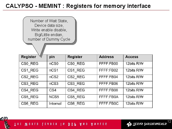
CALYPSO - MEMINT : Registers for memory interface Number of Wait State, Device data size, Write enable disable, Big/Little endian, number of Dummy Cycle 12
Calypso - Interrupt Handler 13
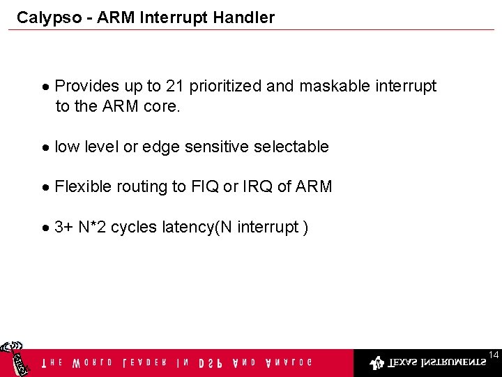
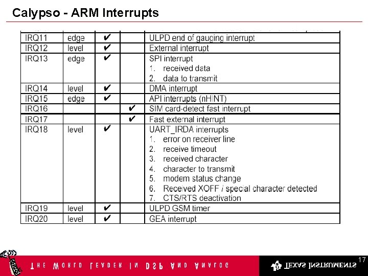
Calypso - ARM Interrupt Handler · Provides up to 21 prioritized and maskable interrupt to the ARM core. · low level or edge sensitive selectable · Flexible routing to FIQ or IRQ of ARM · 3+ N*2 cycles latency(N interrupt ) 14
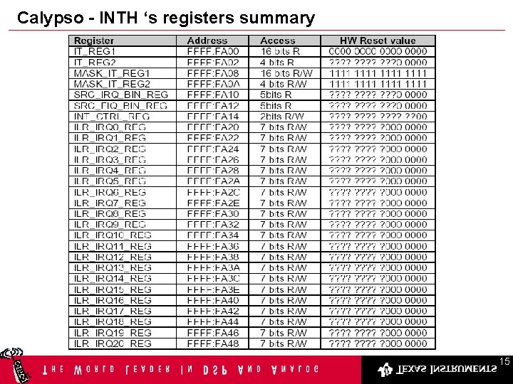
Calypso - INTH ‘s registers summary 15
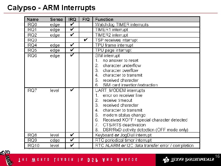
Calypso - ARM Interrupts 16
Calypso - ARM Interrupts 17
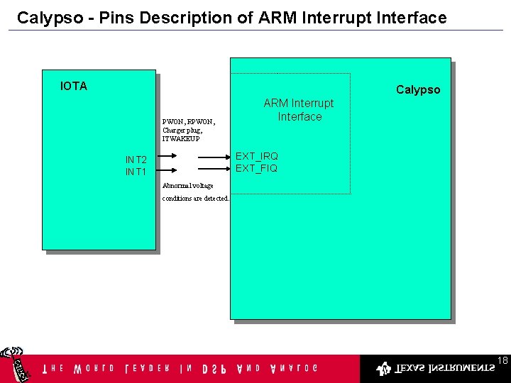
Calypso - Pins Description of ARM Interrupt Interface IOTA Calypso PWON, RPWON, Charger plug, ITWAKEUP ARM Interrupt Interface EXT_IRQ EXT_FIQ INT 2 INT 1 Abnormal voltage conditions are detected. 18
Calypso - Clocks Generator and Control CLKM 19
Calypso - CLKM : Features · Generate and control clocks distribution to the ARM core, Lead core, internal and external peripherals. · Control reset signals of ARM core, LEAD core, internal and external peripherals. · Control deep low power mode of external FLASH 20
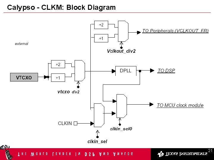
Calypso - CLKM: Block Diagram 21
Calypso - Real Time Clock 22
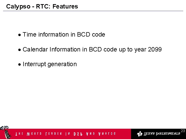
Calypso - RTC: Features · Time information in BCD code · Calendar Information in BCD code up to year 2099 · Interrupt generation 23

Calypso - RTC: Block Diagram 24
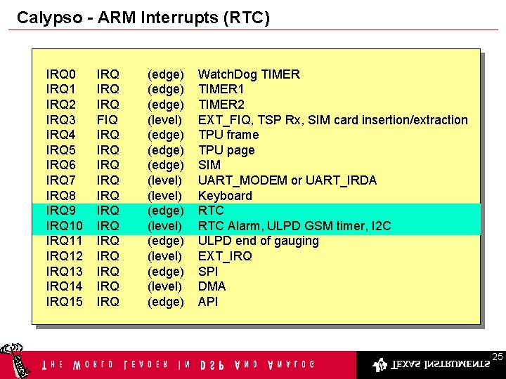
Calypso - ARM Interrupts (RTC) IRQ 0 IRQ 1 IRQ 2 IRQ 3 IRQ 4 IRQ 5 IRQ 6 IRQ 7 IRQ 8 IRQ 9 IRQ 10 IRQ 11 IRQ 12 IRQ 13 IRQ 14 IRQ 15 IRQ IRQ FIQ IRQ IRQ IRQ (edge) (edge) (level) (edge) (level) (edge) Watch. Dog TIMER 1 TIMER 2 EXT_FIQ, TSP Rx, SIM card insertion/extraction TPU frame TPU page SIM UART_MODEM or UART_IRDA Keyboard RTC Alarm, ULPD GSM timer, I 2 C ULPD end of gauging EXT_IRQ SPI DMA API 25
Calypso - Ultra Low Power Down Controller ULPD Controller 26
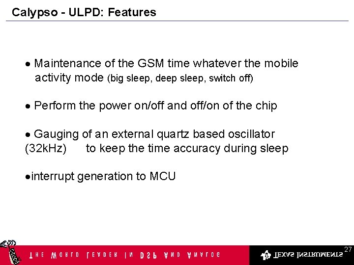
Calypso - ULPD: Features · Maintenance of the GSM time whatever the mobile activity mode (big sleep, deep sleep, switch off) · Perform the power on/off and off/on of the chip · Gauging of an external quartz based oscillator (32 k. Hz) to keep the time accuracy during sleep ·interrupt generation to MCU 27
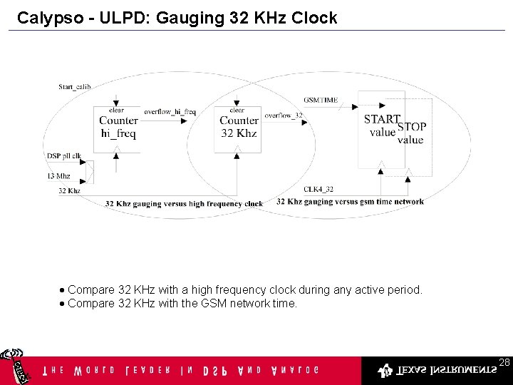
Calypso - ULPD: Gauging 32 KHz Clock · Compare 32 KHz with a high frequency clock during any active period. · Compare 32 KHz with the GSM network time. 28
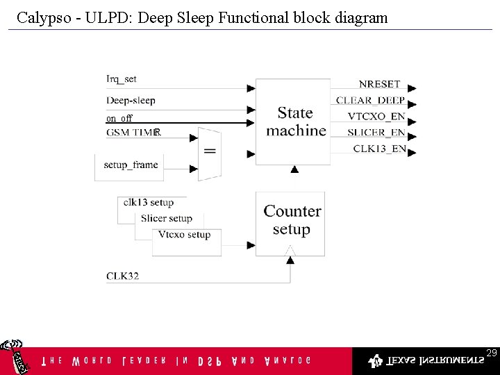
Calypso - ULPD: Deep Sleep Functional block diagram on_off R 29
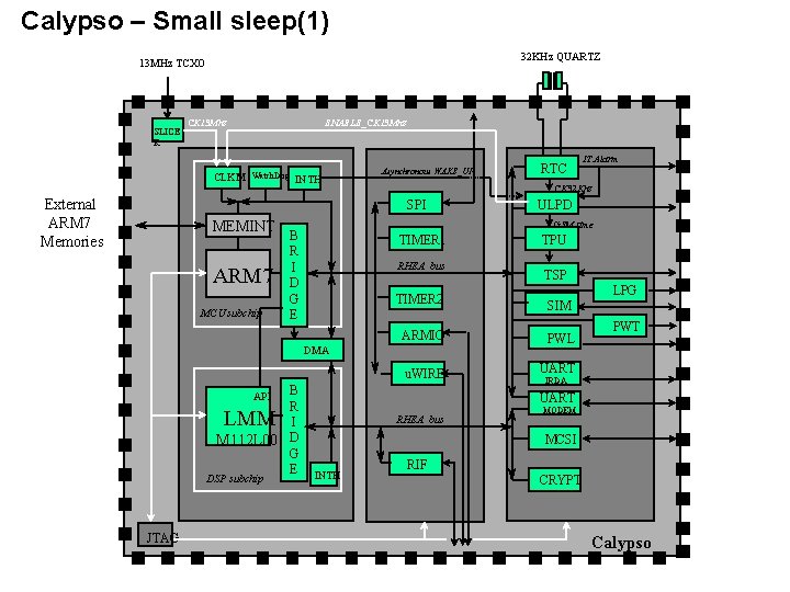
Calypso – Small sleep(1) 32 KHz QUARTZ 13 MHz TCXO SLICE R CK 13 Mhz CLKM External ARM 7 Memories ENABLE_CK 13 Mhz Watch. Dog INTH Asynchronous WAKE_UP ARM 7 MCU subchip TIMER 1 RHEA bus TIMER 2 TSP SIM PWL u. WIRE UART LPG PWT IRDA UART LMM JTAG TPU ARMIO DMA DSP subchip ULPD GSM time B R I D G E B API R I D M 112 L 00 G E IT Alarm CK 32 Khz SPI MEMINT RTC RHEA bus MODEM MCSI INTH RIF CRYPT Calypso
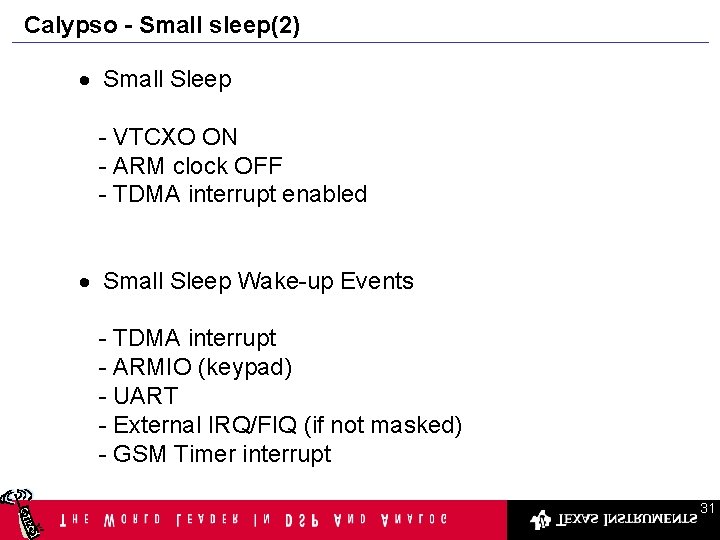
Calypso - Small sleep(2) · Small Sleep - VTCXO ON - ARM clock OFF - TDMA interrupt enabled · Small Sleep Wake-up Events - TDMA interrupt - ARMIO (keypad) - UART - External IRQ/FIQ (if not masked) - GSM Timer interrupt 31
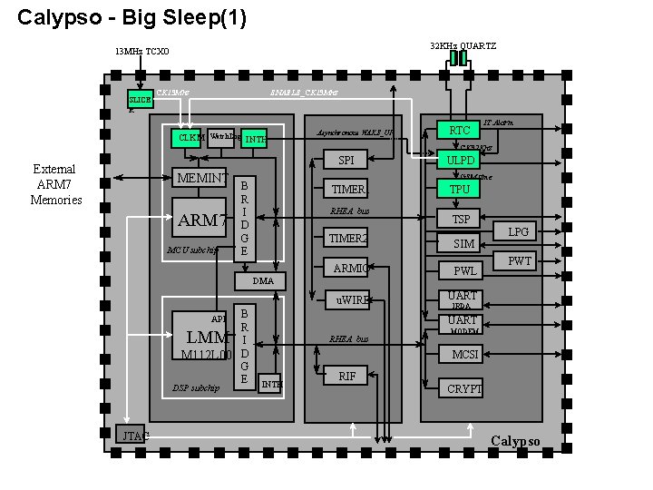
Calypso - Big Sleep(1) 32 KHz QUARTZ 13 MHz TCXO SLICE R CK 13 Mhz CLKM ENABLE_CK 13 Mhz Watch. Dog INTH Asynchronous WAKE_UP MEMINT ARM 7 MCU subchip TIMER 1 RHEA bus TIMER 2 TSP SIM PWL u. WIRE UART API LPG PWT IRDA UART LMM JTAG TPU ARMIO DMA DSP subchip ULPD GSM time B R I D G E B R I M 112 L 00 D G E IT Alarm CK 32 Khz SPI External ARM 7 Memories RTC RHEA bus MODEM MCSI INTH RIF CRYPT Calypso
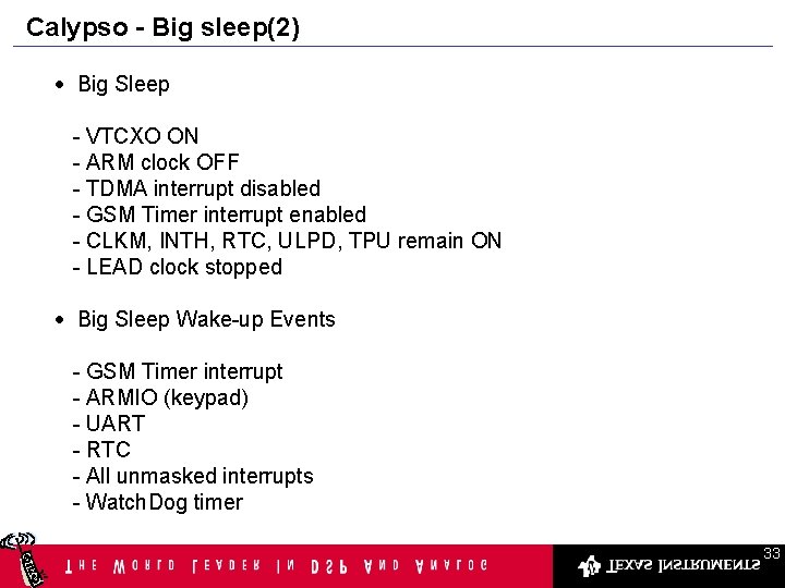
Calypso - Big sleep(2) · Big Sleep - VTCXO ON - ARM clock OFF - TDMA interrupt disabled - GSM Timer interrupt enabled - CLKM, INTH, RTC, ULPD, TPU remain ON - LEAD clock stopped · Big Sleep Wake-up Events - GSM Timer interrupt - ARMIO (keypad) - UART - RTC - All unmasked interrupts - Watch. Dog timer 33
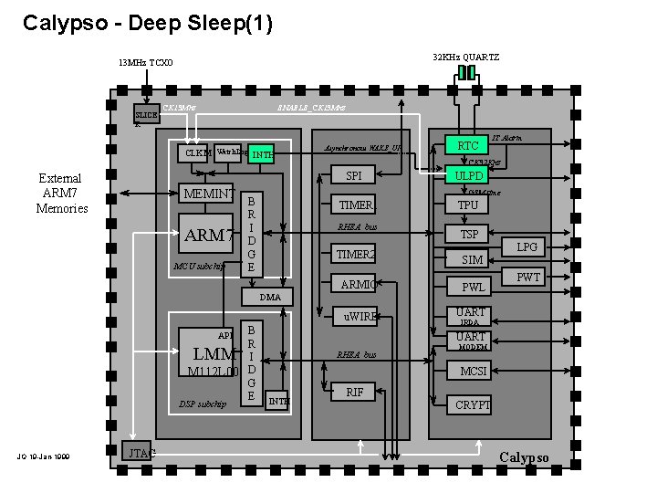
Calypso - Deep Sleep(1) 32 KHz QUARTZ 13 MHz TCXO SLICE R CK 13 Mhz CLKM ENABLE_CK 13 Mhz Watch. Dog INTH Asynchronous WAKE_UP MEMINT ARM 7 MCU subchip TIMER 1 RHEA bus TIMER 2 SIM u. WIRE UART LPG PWT IRDA UART LMM JTAG TSP PWL API JQ 19 -Jan-1999 TPU ARMIO DMA DSP subchip ULPD GSM time B R I D G E B R I M 112 L 00 D G E IT Alarm CK 32 Khz SPI External ARM 7 Memories RTC RHEA bus MODEM MCSI INTH RIF CRYPT Calypso
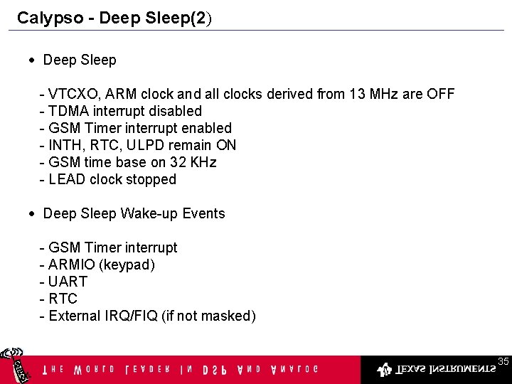
Calypso - Deep Sleep(2) · Deep Sleep - VTCXO, ARM clock and all clocks derived from 13 MHz are OFF - TDMA interrupt disabled - GSM Timer interrupt enabled - INTH, RTC, ULPD remain ON - GSM time base on 32 KHz - LEAD clock stopped · Deep Sleep Wake-up Events - GSM Timer interrupt - ARMIO (keypad) - UART - RTC - External IRQ/FIQ (if not masked) 35
CALYPSO - Serial Port Interface * DO NOT COPY * 36
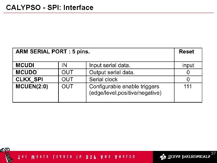
CALYPSO - SPI: Interface 37
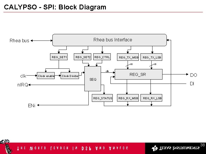
CALYPSO - SPI: Block Diagram Rhea bus Interface Rhea bus REG_SET 1 REG_SET 2 REG_CTRL REG_TX_MSB REG_TX_LSB 16 clk Clock enable Clock Divider 16 REG_SR SEQ DI n. IRQ REG_STATUS DO REG_RX_MSB REG_RX_LSB ENi 38
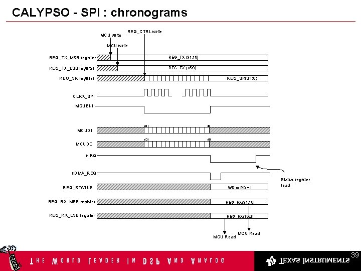
CALYPSO - SPI : chronograms MCU write REG_CTRL write MCU write REG_TX_MSB register REG_TX (31: 16) REG_TX_LSB register REG_TX (15: 0) REG_SR register REG_SR(31: 0) CLKX_SPI MCUENi d 31 d 0 MCUDI MCUDO n. IRQ n. DMA_REQ REG_STATUS WR or RD =1 REG_RX_MSB register REG_RX(31: 16) REG_RX_LSB register REG_RX(15: 0) MCU Read Status register read MCU Read 39
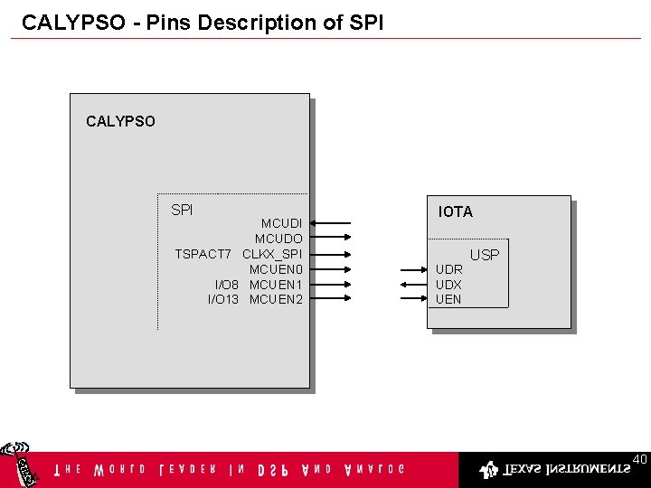
CALYPSO - Pins Description of SPI CALYPSO SPI MCUDO TSPACT 7 CLKX_SPI MCUEN 0 I/O 8 MCUEN 1 I/O 13 MCUEN 2 IOTA UDR UDX UEN USP 40
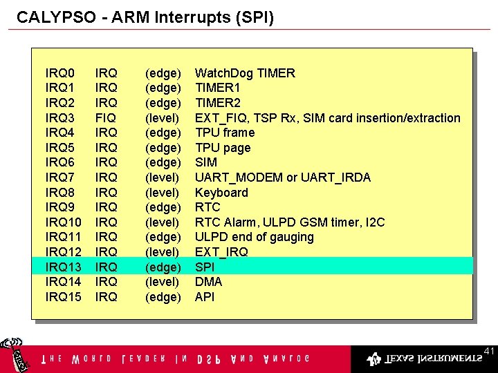
CALYPSO - ARM Interrupts (SPI) IRQ 0 IRQ 1 IRQ 2 IRQ 3 IRQ 4 IRQ 5 IRQ 6 IRQ 7 IRQ 8 IRQ 9 IRQ 10 IRQ 11 IRQ 12 IRQ 13 IRQ 14 IRQ 15 IRQ IRQ FIQ IRQ IRQ IRQ (edge) (edge) (level) (edge) (level) (edge) Watch. Dog TIMER 1 TIMER 2 EXT_FIQ, TSP Rx, SIM card insertion/extraction TPU frame TPU page SIM UART_MODEM or UART_IRDA Keyboard RTC Alarm, ULPD GSM timer, I 2 C ULPD end of gauging EXT_IRQ SPI DMA API 41
Calypso - Radio Interface * DO NOT COPY * 42
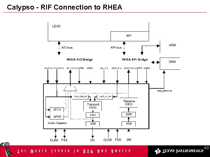
Calypso - RIF Connection to RHEA 43
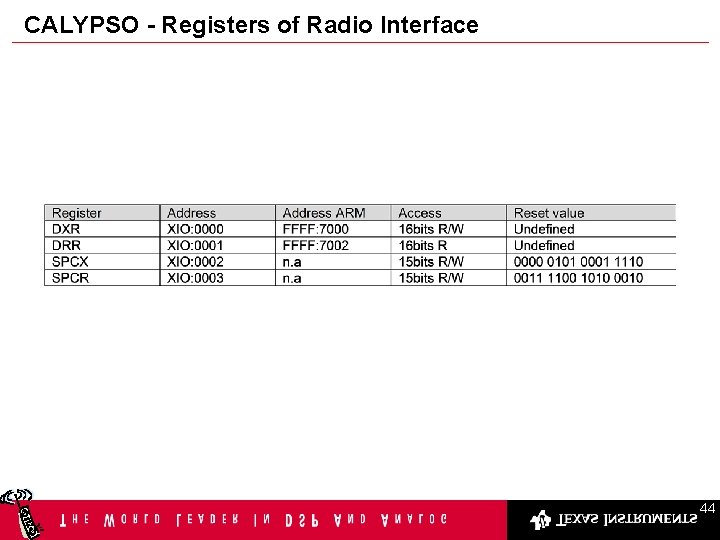
CALYPSO - Registers of Radio Interface 44
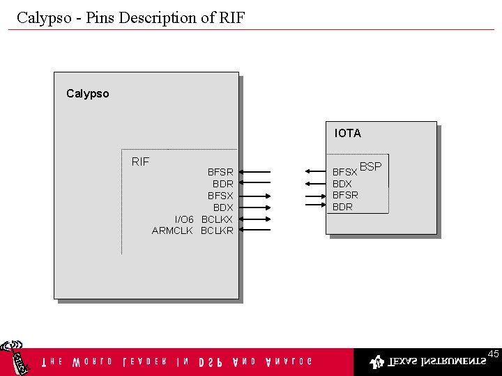
Calypso - Pins Description of RIF Calypso IOTA RIF BFSR BDR BFSX BDX I/O 6 BCLKX ARMCLK BCLKR BFSX BSP BDX BFSR BDR 45
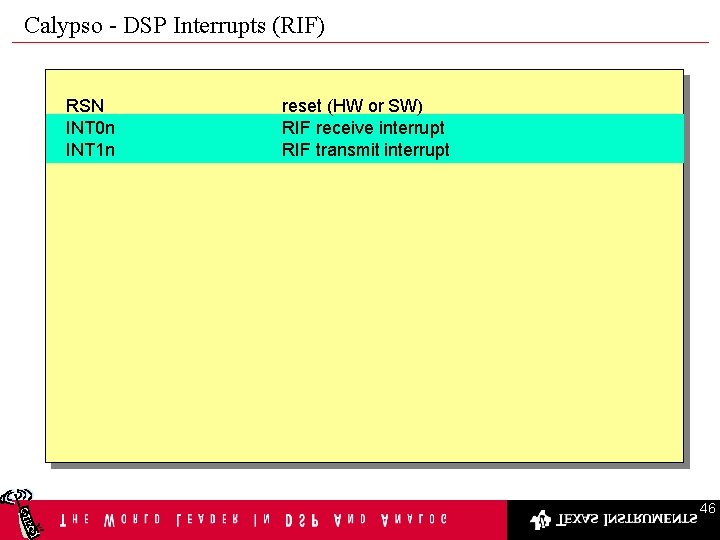
Calypso - DSP Interrupts (RIF) RSN INT 0 n INT 1 n reset (HW or SW) RIF receive interrupt RIF transmit interrupt 46
CALYPSO - Time Processing Unit * DO NOT COPY * 47
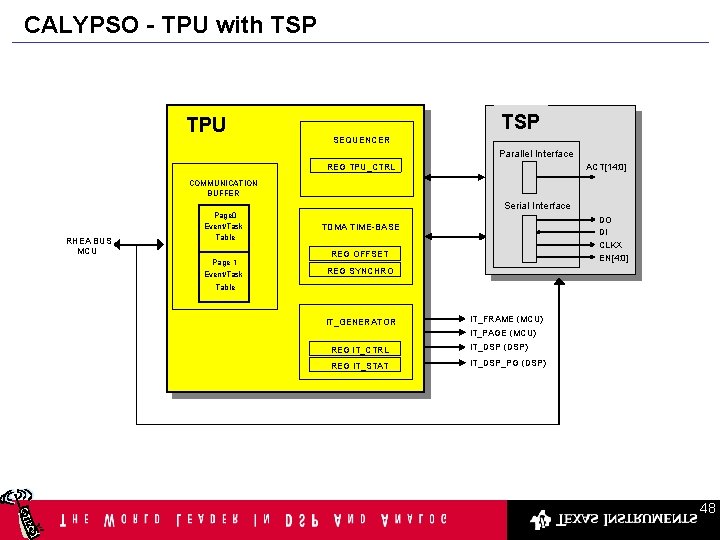
CALYPSO - TPU with TSP TPU TSP SEQUENCER Parallel Interface REG TPU_CTRL ACT[14: 0] COMMUNICATION BUFFER RHEA BUS MCU Page 0 Event/Task Table Page 1 Event/Task Serial Interface DO DI CLKX EN[4: 0] TDMA TIME-BASE REG OFFSET REG SYNCHRO Table IT_GENERATOR IT_FRAME (MCU) IT_PAGE (MCU) REG IT_CTRL IT_DSP (DSP) REG IT_STAT IT_DSP_PG (DSP) 48
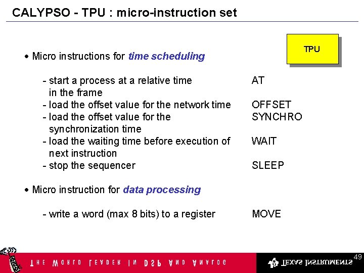
CALYPSO - TPU : micro-instruction set TPU · Micro instructions for time scheduling - start a process at a relative time in the frame - load the offset value for the network time - load the offset value for the synchronization time - load the waiting time before execution of next instruction - stop the sequencer AT OFFSET SYNCHRO WAIT SLEEP · Micro instruction for data processing - write a word (max 8 bits) to a register MOVE 49
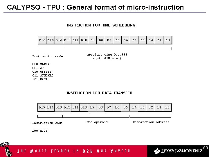
CALYPSO - TPU : General format of micro-instruction INSTRUCTION FOR TIME SCHEDULING b 15 b 14 b 13 b 12 b 11 b 10 b 9 Instruction code 000 001 010 011 101 b 8 b 7 b 6 b 5 b 4 b 3 b 2 b 1 b 0 Absolute time 0. . 4999 (qbit GSM step) SLEEP AT OFFSET SYNCHRO WAIT INSTRUCTION FOR DATA TRANSFER b 15 b 14 b 13 b 12 b 11 b 10 b 9 Instruction code b 8 b 7 Data operand b 6 b 5 b 4 Destination address 100 MOVE 50
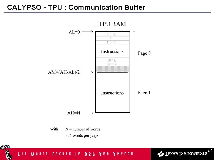
CALYPSO - TPU : Communication Buffer 256 words per page 51
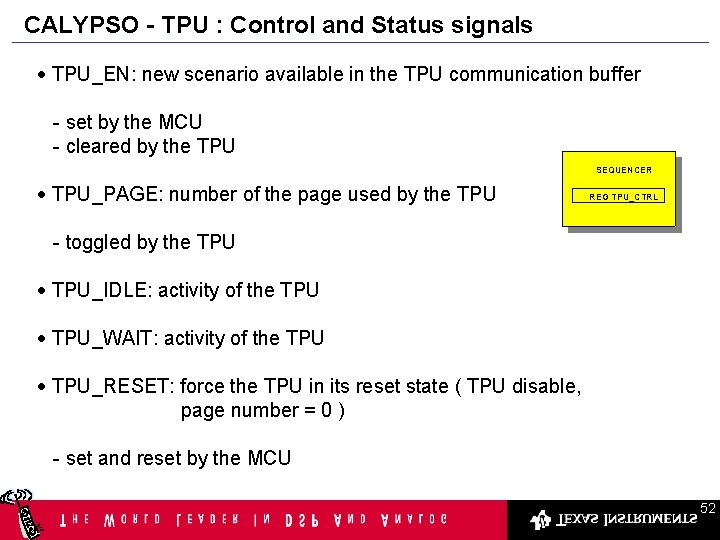
CALYPSO - TPU : Control and Status signals · TPU_EN: new scenario available in the TPU communication buffer - set by the MCU - cleared by the TPU SEQUENCER · TPU_PAGE: number of the page used by the TPU REG TPU_CTRL - toggled by the TPU · TPU_IDLE: activity of the TPU · TPU_WAIT: activity of the TPU · TPU_RESET: force the TPU in its reset state ( TPU disable, page number = 0 ) - set and reset by the MCU 52
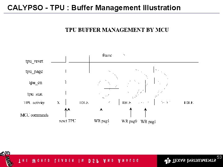
CALYPSO - TPU : Buffer Management Illustration 53
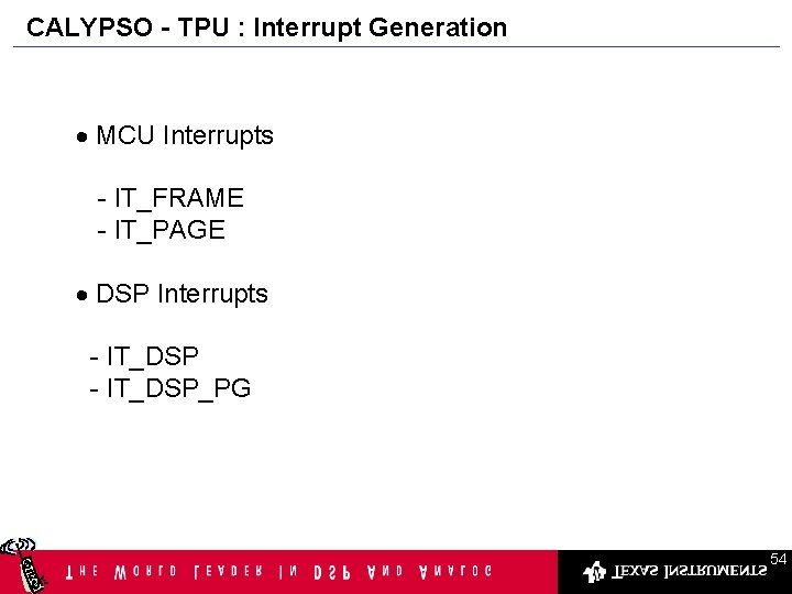
CALYPSO - TPU : Interrupt Generation · MCU Interrupts - IT_FRAME - IT_PAGE · DSP Interrupts - IT_DSP_PG 54
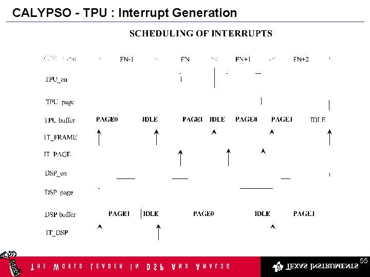
CALYPSO - TPU : Interrupt Generation 55
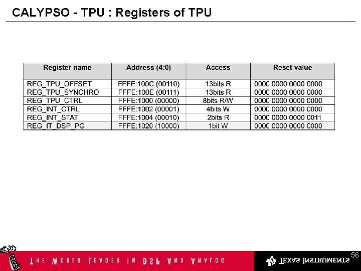
CALYPSO - TPU : Registers of TPU 56
CALYPSO - Time Serial Port * DO NOT COPY * 57
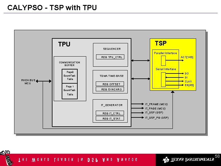
CALYPSO - TSP with TPU TSP SEQUENCER Parallel Interface REG TPU_CTRL ACT[14: 0] COMMUNICATION BUFFER RHEA BUS MCU Page 0 Event/Task Table Page 1 Event/Task Serial Interface DO DI CLKX EN[4: 0] TDMA TIME-BASE REG OFFSET REG SYNCHRO Table IT_GENERATOR IT_FRAME (MCU) IT_PAGE (MCU) REG IT_CTRL IT_DSP (DSP) REG IT_STAT IT_DSP_PG (DSP) 58
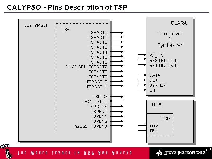
CALYPSO - Pins Description of TSP CALYPSO CLARA TSPACT 0 TSPACT 1 TSPACT 2 TSPACT 3 TSPACT 4 TSPACT 5 TSPACT 6 CLKX_SPI TSPACT 7 TSPACT 8 TSPACT 9 TSPACT 10 TSPACT 11 TSPDO I/O 4 TSPDI TSPCLKX TSPEN 0 TSPEN 1 TSPEN 2 n. SCS 2 TSPEN 3 Transceiver & Synthesizer PA_ON RX 900/TX 1800 RX 1800/TX 900 DATA CLK SYN_EN EN IOTA TSP TDR TEN 59
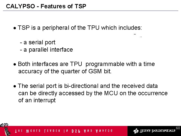
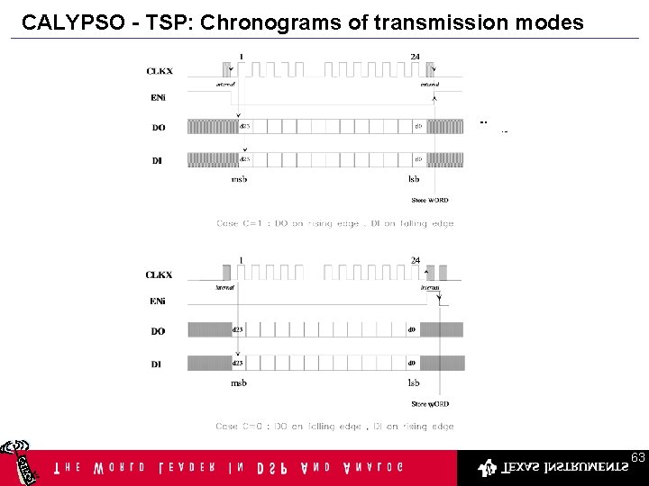
CALYPSO - Features of TSP · TSP is a peripheral of the TPU which includes: - a serial port - a parallel interface · Both interfaces are TPU programmable with a time accuracy of the quarter of GSM bit. · The serial port is bi-directional and the received data can be directly accessed by the MCU on the occurrence of an interrupt 60
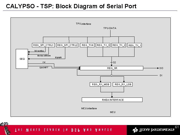
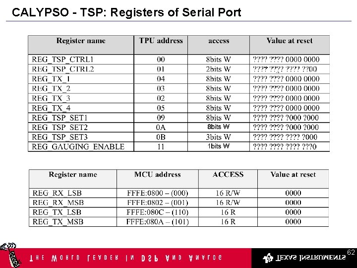
CALYPSO - TSP: Block Diagram of Serial Port TPU interface TPU-DATA REG_SPI_CTRL 1 REG_SPI_CTRL 2 REG_TX 4 REG_TX_3 REG_TX_2 REG_TX_1 bit number device address SEQ RD/WR 32 CK LD/SHIFT REG_SR DO DI REG_RX_MSB REG_RX_LSB RHEA INTERFACE MCU interface MCU 61
CALYPSO - TSP: Registers of Serial Port 62
CALYPSO - TSP: Chronograms of transmission modes 63
CALYPSO - TSP: Serial Transmission Time 64
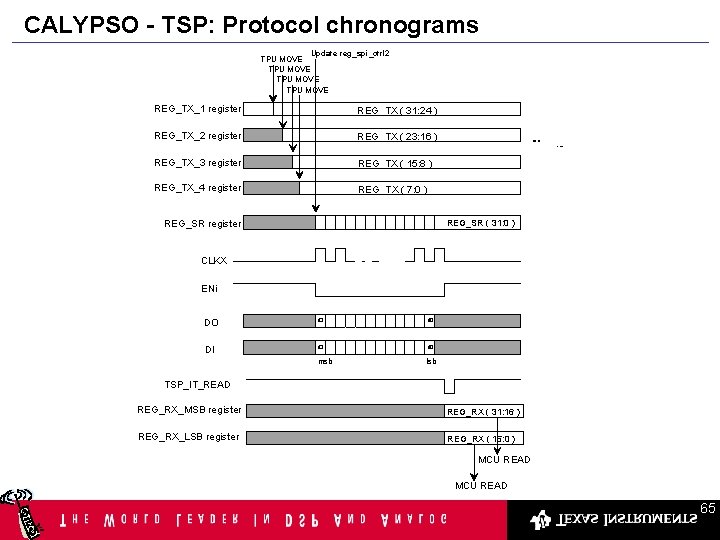
CALYPSO - TSP: Protocol chronograms Update reg_spi_ctrl 2 TPU MOVE REG_TX_1 register REG_TX ( 31: 24 ) REG_TX_2 register REG_TX ( 23: 16 ) REG_TX_3 register REG_TX ( 15: 8 ) REG_TX_4 register REG_TX ( 7: 0 ) REG_SR ( 31: 0 ) REG_SR register CLKX ENi DO d 31 d 0 DI d 31 d 0 msb lsb TSP_IT_READ REG_RX_MSB register REG_RX ( 31: 16 ) REG_RX_LSB register REG_RX ( 15: 0 ) MCU READ 65
CALYPSO - ARMIO ARM I/O 66
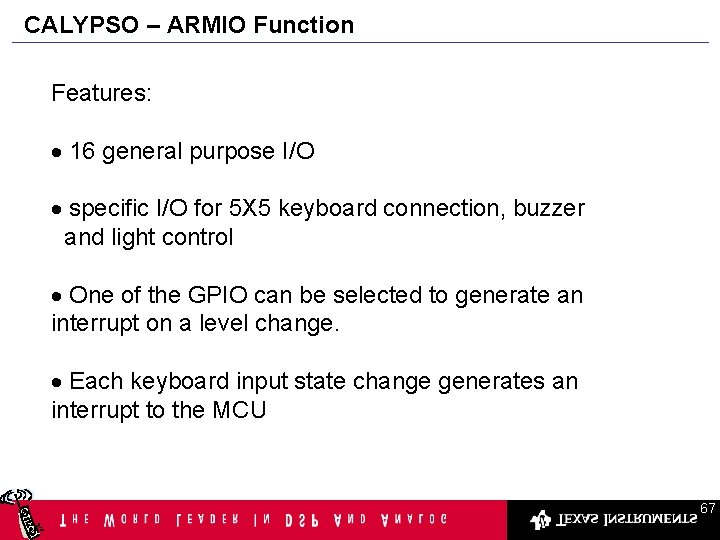
CALYPSO – ARMIO Function Features: · 16 general purpose I/O · specific I/O for 5 X 5 keyboard connection, buzzer and light control · One of the GPIO can be selected to generate an interrupt on a level change. · Each keyboard input state change generates an interrupt to the MCU 67
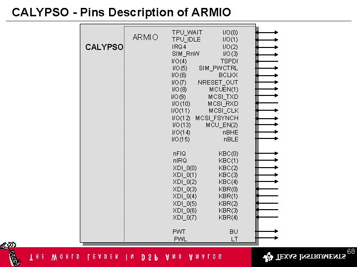
CALYPSO - Pins Description of ARMIO CALYPSO TPU_WAIT I/O(0) TPU_IDLE I/O(1) IRQ 4 I/O(2) SIM_Rn. W I/O(3) I/O(4) TSPDI I/O(5) SIM_PWCTRL I/O(6) BCLKX I/O(7) NRESET_OUT I/O(8) MCUEN(1) I/O(9) MCSI_TXD I/O(10) MCSI_RXD I/O(11) MCSI_CLK I/O(12) MCSI_FSYNCH I/O(13) MCU_EN(2) I/O(14) n. BHE I/O(15) n. BLE n. FIQ n. IRQ XDI_0(0) XDI_0(1) XDI_0(2) XDI_0(3) XDI_0(4) XDI_0(5) XDI_0(6) XDI_0(7) PWT PWL KBC(0) KBC(1) KBC(2) KBC(3) KBC(4) KBR(0) KBR(1) KBR(2) KBR(3) KBR(4) BU LT 68
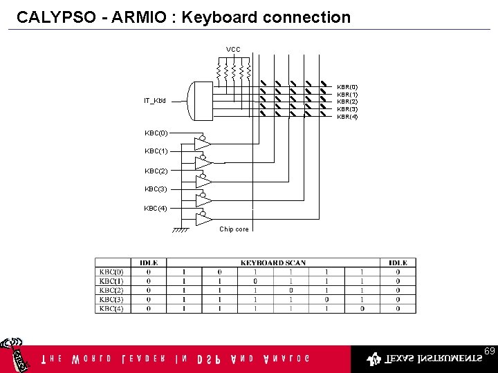
CALYPSO - ARMIO : Keyboard connection VCC KBR(0) KBR(1) KBR(2) KBR(3) KBR(4) IT_Kbd KBC(0) KBC(1) KBC(2) KBC(3) KBC(4) Chip core 69
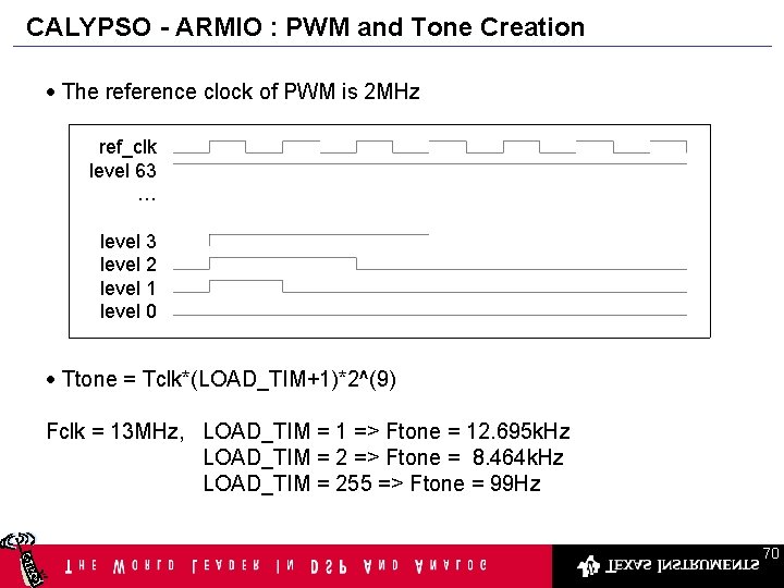
CALYPSO - ARMIO : PWM and Tone Creation · The reference clock of PWM is 2 MHz ref_clk level 63 … level 3 level 2 level 1 level 0 · Ttone = Tclk*(LOAD_TIM+1)*2^(9) Fclk = 13 MHz, LOAD_TIM = 1 => Ftone = 12. 695 k. Hz LOAD_TIM = 2 => Ftone = 8. 464 k. Hz LOAD_TIM = 255 => Ftone = 99 Hz 70
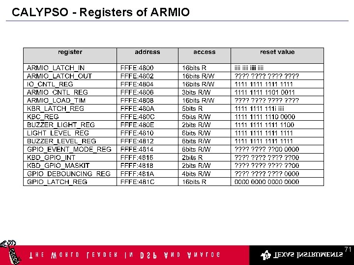
CALYPSO - Registers of ARMIO 71
CALYPSO – General Purpose Timer 72
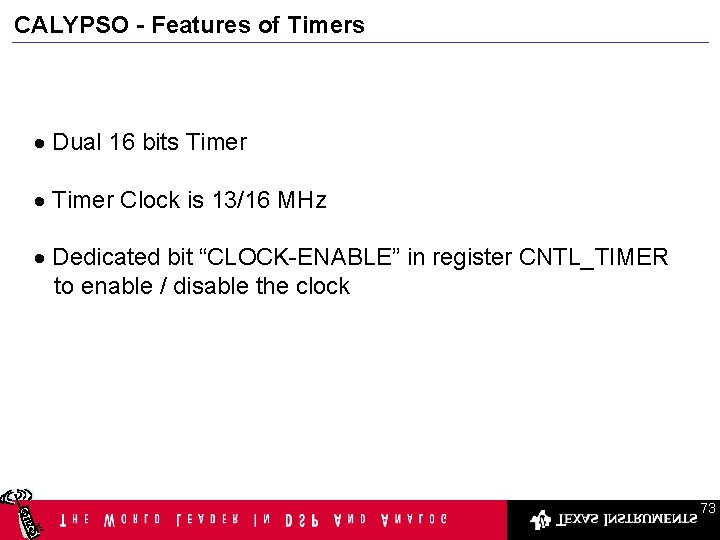
CALYPSO - Features of Timers · Dual 16 bits Timer · Timer Clock is 13/16 MHz · Dedicated bit “CLOCK-ENABLE” in register CNTL_TIMER to enable / disable the clock 73
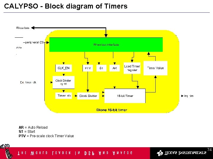
CALYPSO - Block diagram of Timers AR = Auto Reload ST = Start PTV = Pre-scale clock Timer Value 74
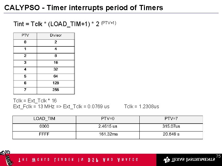
CALYPSO - Timer interrupts period of Timers Tint = Tclk * (LOAD_TIM+1) * 2 (PTV+1) Tclk = Ext_Tclk * 16 Ext_Fclk = 13 MHz => Ext_Tclk = 0. 0769 us Tclk = 1. 2308 us 75
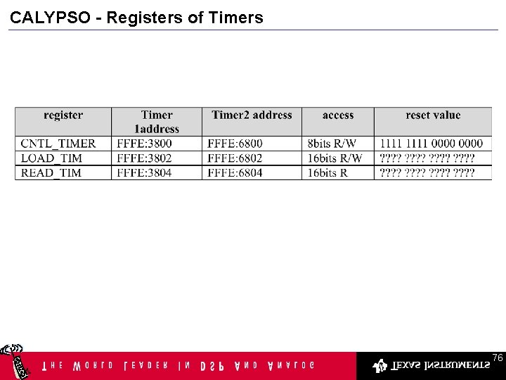
CALYPSO - Registers of Timers 76
CALYPSO – Watchdog Timer 77
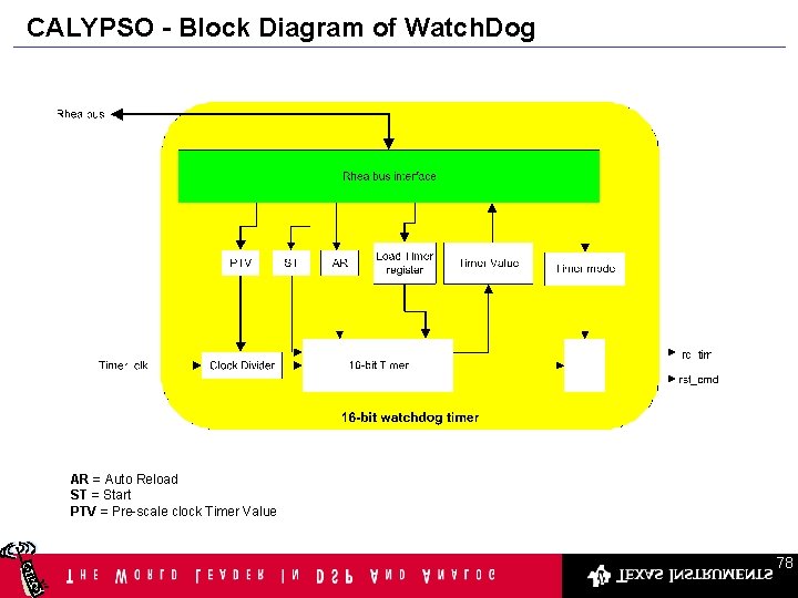
CALYPSO - Block Diagram of Watch. Dog AR = Auto Reload ST = Start PTV = Pre-scale clock Timer Value 78
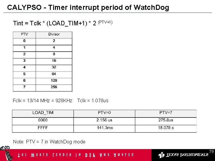
CALYPSO - Timer interrupt period of Watch. Dog Tint = Tclk * (LOAD_TIM+1) * 2 (PTV+1) Fclk = 13/14 MHz = 928 KHz Tclk = 1. 078 us Note: PTV = 7 in Watch. Dog mode 79
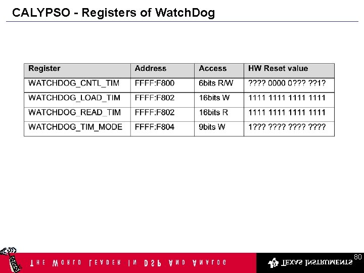
CALYPSO - Registers of Watch. Dog 80
CALYPSO – uwire Uwire 81
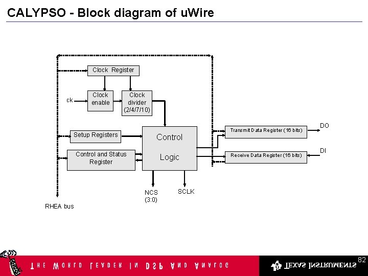
CALYPSO - Block diagram of u. Wire Clock Register ck Clock enable Clock divider (2/4/7/10) Setup Registers Transmit Data Register (16 bits) Control and Status Register RHEA bus DO Logic NCS (3: 0) Receive Data Register (16 bits) DI SCLK 82
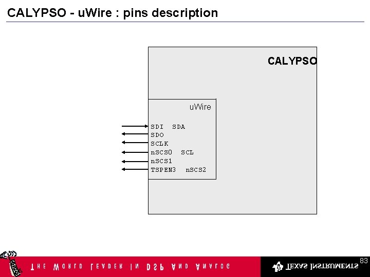
CALYPSO - u. Wire : pins description CALYPSO u. Wire SDI SDA SDO SCLK n. SCS 0 SCL n. SCS 1 TSPEN 3 n. SCS 2 83
CALYPSO – I 2 C Interface 84
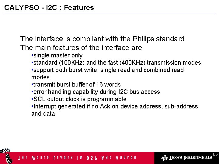
CALYPSO - I 2 C : Features The interface is compliant with the Philips standard. The main features of the interface are: • single master only • standard (100 KHz) and the fast (400 KHz) transmission modes • support both burst write, single read and combined read modes • transmit burst buffer of 16 words • error handling capability during I 2 C bus access • SCL output clock is programmable • Interrupt generated if no Ack on device address, sub-address and data 85
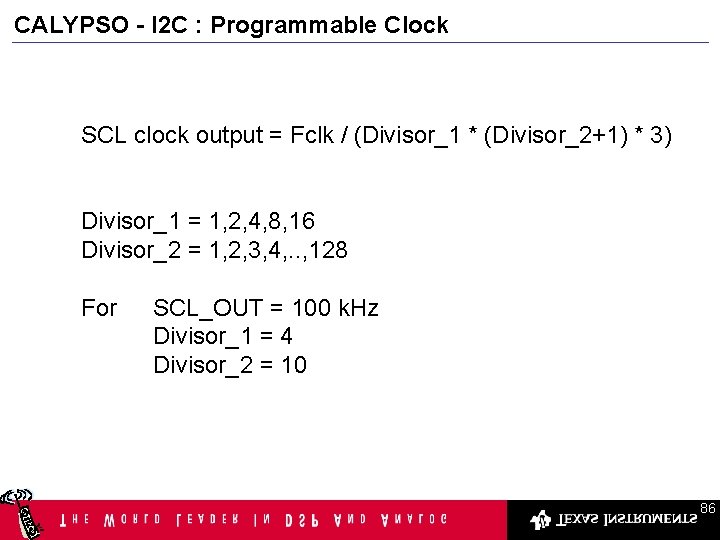
CALYPSO - I 2 C : Programmable Clock SCL clock output = Fclk / (Divisor_1 * (Divisor_2+1) * 3) Divisor_1 = 1, 2, 4, 8, 16 Divisor_2 = 1, 2, 3, 4, . . , 128 For SCL_OUT = 100 k. Hz Divisor_1 = 4 Divisor_2 = 10 86
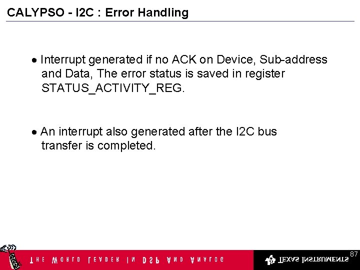
CALYPSO - I 2 C : Error Handling · Interrupt generated if no ACK on Device, Sub-address and Data, The error status is saved in register STATUS_ACTIVITY_REG. · An interrupt also generated after the I 2 C bus transfer is completed. 87
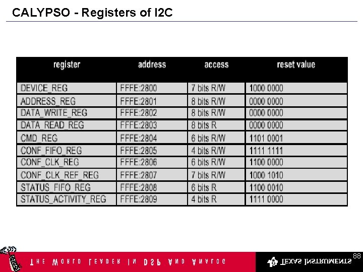
CALYPSO - Registers of I 2 C 88
CALYPSO – UART 89
CALYPSO – UART Module – UART/Ir. DA module: • an Ir. DA SIR protocol encoder/decoder can be optionally selected to manage the RXIR and TXIR signals to an Ir. DA transceiver. – UART/modem module: • incorporates an autobauding mechanism and the possibility to connect dynamically the UART/modem to the DSP or MCU Rhea buses. 90
CALYPSO - UART Common Features • 64 -word deep FIFO for received/transmitted characters • The trigger levels for the FIFOs are independently • Configurable to send even, odd or no parity and 1, 1½ or 2 stop bits. • They generate their own baud rate based upon a programmable divisor. 91
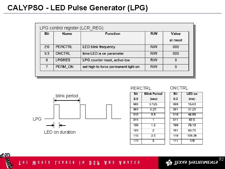
CALYPSO - LED Pulse Generator (LPG) LPG control register (LCR_REG) PERCTRL ONCTRL blink period LPG LED on duration 92
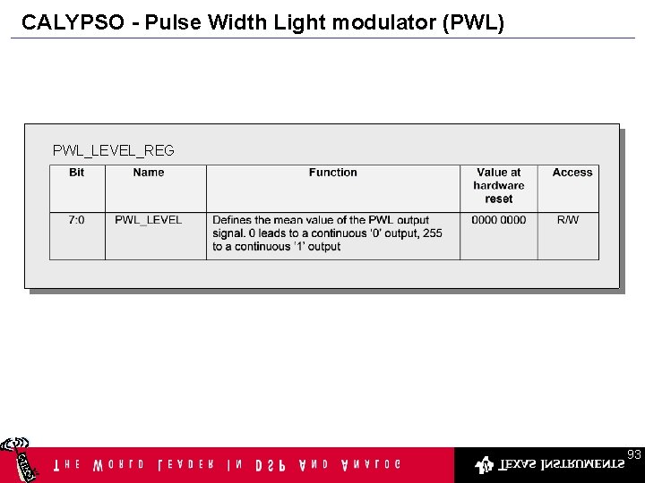
CALYPSO - Pulse Width Light modulator (PWL) PWL_LEVEL_REG 93
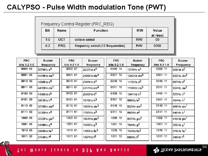
CALYPSO - Pulse Width modulation Tone (PWT) Frequency Control Register (FRC_REG) 94

Thank you! 95
- Slides: 95