Fundamentals of High Speed AnalogtoDigital Converters Texas Instruments
- Slides: 65

Fundamentals of High Speed Analog-to-Digital Converters Texas Instruments High Speed Data Converters Nov. 2012 1 TI Information – NDA Required

Outline • ADC specifications – SNR, ENOB – SFDR, HD 2, HD 3 • FFT Process gain • ADC full-scale calculation • Oversampling, undersampling & aliasing • Clocking high speed ADCs – phase noise, jitter, slew rate • SNR & SFDR degradation over input frequency • Improving ADC SNR & SFDR 2 TI Information – NDA Required

ADC Specifications 3 TI Information – NDA Required

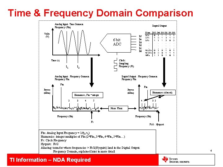
Time & Frequency Domain Comparison Analog Input- Time Domain Frequency (Fin) Digital Output Volts (V) D 5 D 4 D 3 D 2 D 1 D 0 6 bit ADC Time (s) t 1 Clock: Sampling Frequency (Fs) t 2 Analog Input - Frequency Domain Frequency Fin Digital Output - Frequency Domain Frequency Fin Power (d. Bm) Harmonics, Fin * integer 2 3 4 Fin Power (d. Bm) Harmonics (aliased) 5 4 5 3 2 Noise Floor Frequency (Hz) Fs Fin: Analog Input Frequency = 1/(t 2 -t 1) Harmonics: integer multiples of Fin (2*Fin, 3*Fin, 4*Fin, 5*Fin…) Fs: Clock Frequency Nyquist: Fs/2 Aliasing: term for where frequencies > Fs/2(Nyquist) land in the Digital Output Frequency Domain, explained later in more detail TI Information – NDA Required Fs/2 - Nyquist 4

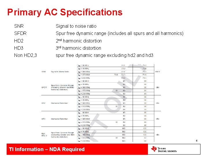
Primary AC Specifications SNR Signal to noise ratio SFDR Spur free dynamic range (includes all spurs and all harmonics) HD 2 2 nd harmonic distortion HD 3 3 rd harmonic distortion Non HD 2, 3 spur free dynamic range excluding hd 2 and hd 3 5 TI Information – NDA Required

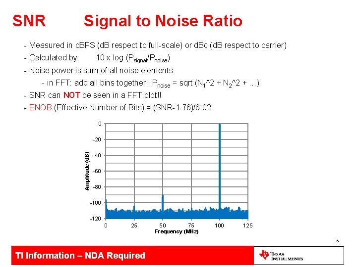
SNR Signal to Noise Ratio - Measured in d. BFS (d. B respect to full-scale) or d. Bc (d. B respect to carrier) - Calculated by: 10 x log (Psignal/Pnoise) - Noise power is sum of all noise elements - in FFT: add all bins together : Pnoise = sqrt (N 1^2 + N 2^2 + …) - SNR can NOT be seen in a FFT plot!! - ENOB (Effective Number of Bits) = (SNR-1. 76)/6. 02 0 Amplitude (d. B) -20 -40 -60 -80 -100 -120 0 25 50 75 Frequency (MHz) 100 125 6 TI Information – NDA Required

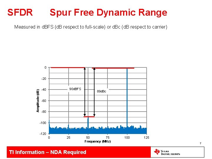
SFDR Spur Free Dynamic Range Measured in d. BFS (d. B respect to full-scale) or d. Bc (d. B respect to carrier) 0 Amplitude (d. B) -20 90 d. BFS -40 89 d. Bc -60 -80 -100 -120 0 25 50 75 Frequency (MHz) TI Information – NDA Required 100 125 7

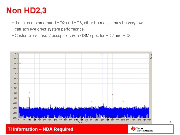
HD 2, 3 2 nd & 3 rd Order Harmonic Distortion • Typically worst spurs in ADC • Separate listing in table allows better system SFDR performance when planning around them • HD 2 shows up at 2 x Fin • HD 3 shows up at 3 x Fin 8 TI Information – NDA Required

Non HD 2, 3 • If user can plan around HD 2 and HD 3, other harmonics may be very low • can achieve great system performance • Customer can use 2 exceptions with GSM spec for HD 2 and HD 3 9 TI Information – NDA Required

FFT Process Gain 10 TI Information – NDA Required

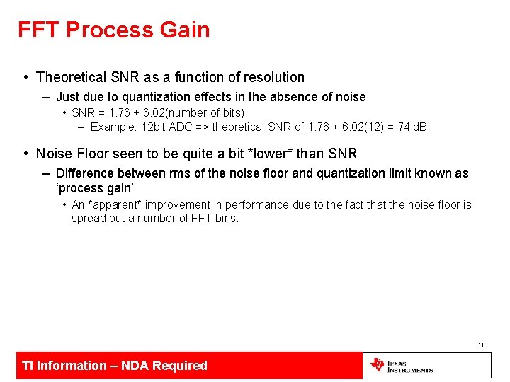
FFT Process Gain • Theoretical SNR as a function of resolution – Just due to quantization effects in the absence of noise • SNR = 1. 76 + 6. 02(number of bits) – Example: 12 bit ADC => theoretical SNR of 1. 76 + 6. 02(12) = 74 d. B • Noise Floor seen to be quite a bit *lower* than SNR – Difference between rms of the noise floor and quantization limit known as ‘process gain’ • An *apparent* improvement in performance due to the fact that the noise floor is spread out a number of FFT bins. 11 TI Information – NDA Required

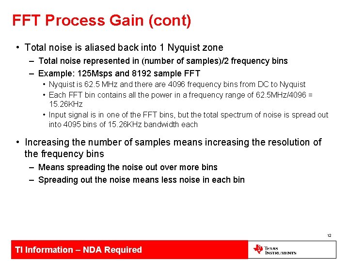
FFT Process Gain (cont) • Total noise is aliased back into 1 Nyquist zone – Total noise represented in (number of samples)/2 frequency bins – Example: 125 Msps and 8192 sample FFT • Nyquist is 62. 5 MHz and there are 4096 frequency bins from DC to Nyquist • Each FFT bin contains all the power in a frequency range of 62. 5 MHz/4096 = 15. 26 KHz • Input signal is in one of the FFT bins, but the total spectrum of noise is spread out into 4095 bins of 15. 26 KHz bandwidth each • Increasing the number of samples means increasing the resolution of the frequency bins – Means spreading the noise out over more bins – Spreading out the noise means less noise in each bin 12 TI Information – NDA Required

FFT Process Gain (cont) • Each doubling of the number of samples pushes the noise floor down by ~3 d. B – Increases the difference between the quantization limit and the noise floor => process gain increases by ~3 d. B Estimated FFT Process Gain = 10 log(number of samples/2) 13 TI Information – NDA Required

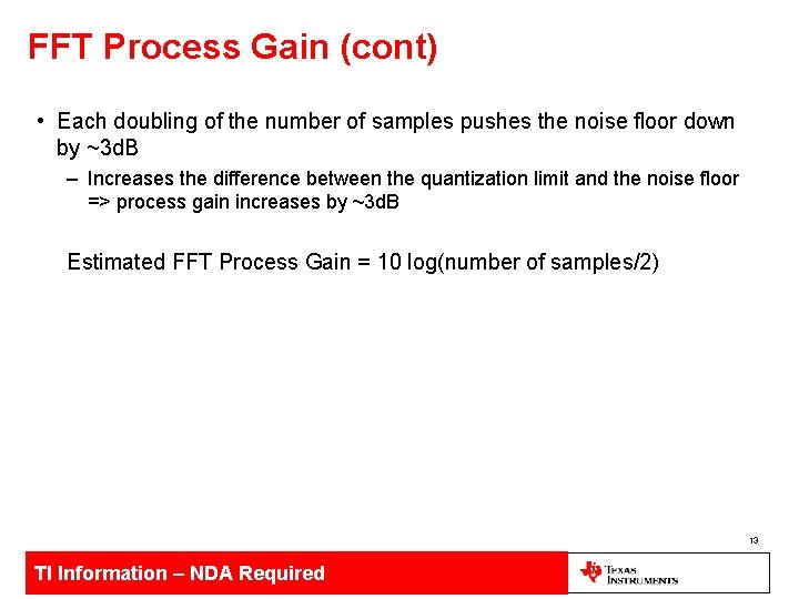
FFT Process Gain – 8192 samples Actual SNR 70. 65 d. BFS Quantization limit 74 d. BFS Noise Floor -106. 78 d. BFS rms • • Process Gain 36. 1 d. BFS Estimated Process Gain = 10 log(4096) = 36. 12 d. B • Theoretical max SNR = 74 d. BFS, but effective number of bits for this device is ~11. 39 bits Actual SNR = 70. 65 d. BFS. Noise floor is at -106. 78 d. BFS, which is 36. 13 d. B below actual SNR 14 TI Information – NDA Required

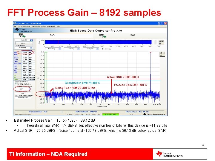
FFT Process Gain – 16384 samples Actual SNR 70. 67 d. BFS Noise Floor -109. 8 d. BFS rms • • Process Gain 39. 2 d. BFS Estimated Process Gain = 10 log(8192) = 39. 13 d. B • Theoretical max SNR = 74 d. BFS, but effective number of bits for this device is ~11. 39 bits Actual SNR = 70. 67 d. BFS. Noise floor is at -109. 8 d. BFS, which is 39. 2 d. B below actual SNR 15 TI Information – NDA Required

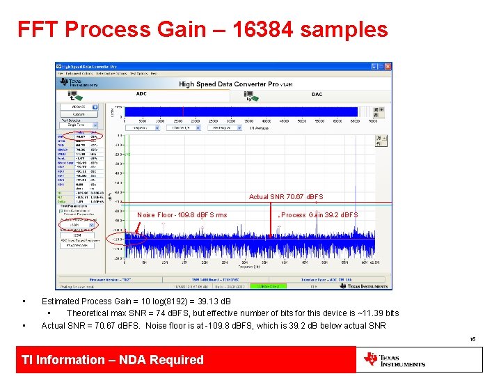
FFT Process Gain – 32768 samples Actual SNR 70. 68 d. BFS Noise Floor -112. 82 d. BFS rms • • Process Gain 42. 1 d. BFS Estimated Process Gain = 10 log(16384) = 42. 14 d. B • Theoretical max SNR = 74 d. BFS, but effective number of bits for this device is ~11. 39 bits Actual SNR = 70. 68 d. BFS. Noise floor is at -112. 82 d. BFS, which is 42. 14 d. B below actual SNR 16 TI Information – NDA Required

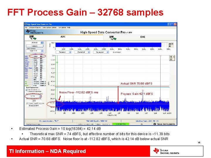
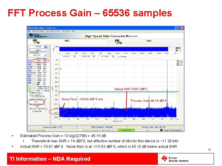
FFT Process Gain – 65536 samples Actual SNR 70. 67 d. BFS Noise Floor -115. 83 d. BFS rms • • Process Gain 45. 15 d. BFS Estimated Process Gain = 10 log(32768) = 45. 15 d. B • Theoretical max SNR = 74 d. BFS, but effective number of bits for this device is ~11. 39 bits Actual SNR = 70. 67 d. BFS. Noise floor is at -115. 83 d. BFS, which is 45. 15 d. B below actual SNR TI Information – NDA Required 17

ADC Full-scale Calucation 18 TI Information – NDA Required

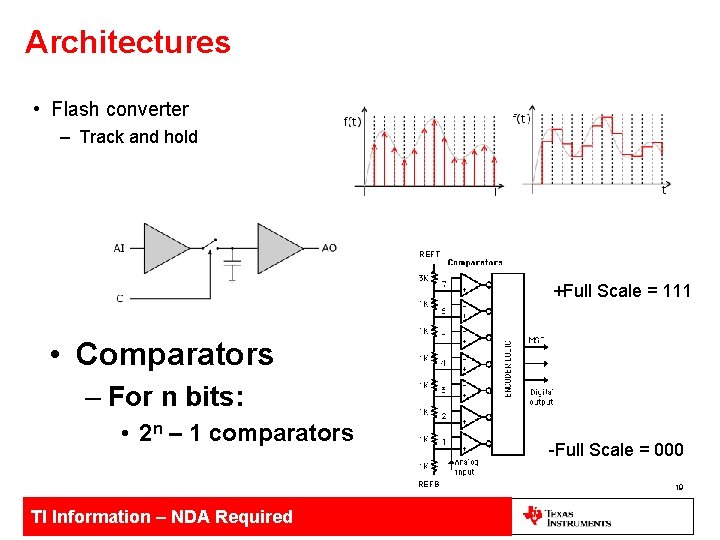
Architectures • Flash converter – Track and hold REFT +Full Scale = 111 • Comparators – For n bits: • 2 n – 1 comparators -Full Scale = 000 REFB TI Information – NDA Required 19

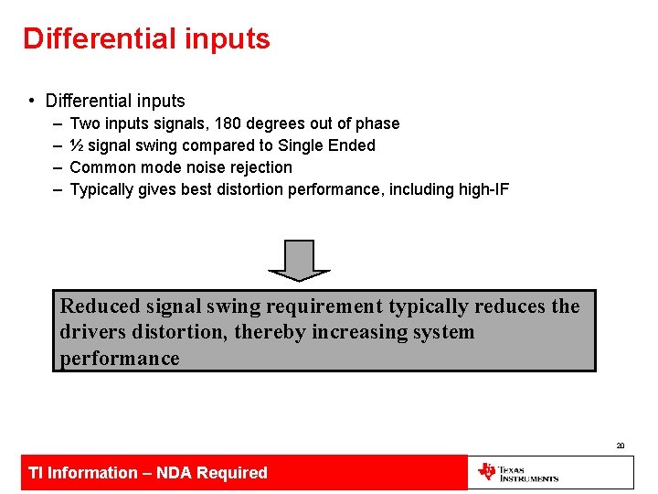
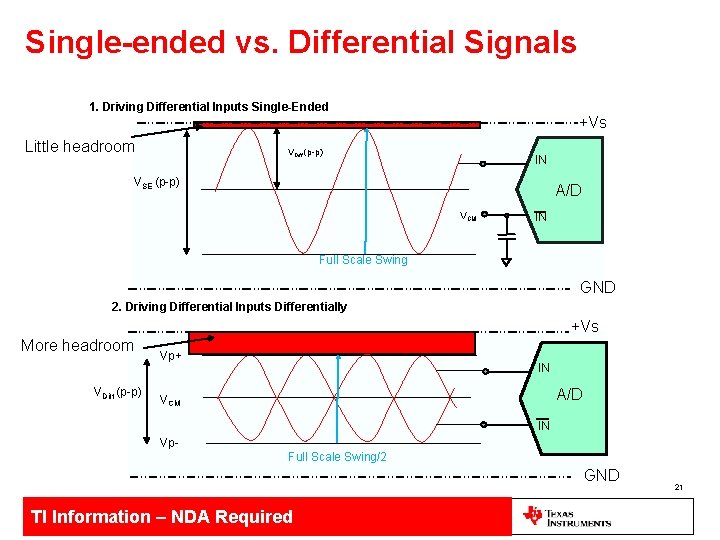
Differential inputs • Differential inputs – – Two inputs signals, 180 degrees out of phase ½ signal swing compared to Single Ended Common mode noise rejection Typically gives best distortion performance, including high-IF Reduced signal swing requirement typically reduces the drivers distortion, thereby increasing system performance 20 TI Information – NDA Required

Single-ended vs. Differential Signals 1. Driving Differential Inputs Single-Ended Little headroom +Vs VDiff (p-p) IN VSE (p-p) A/D VCM IN Full Scale Swing GND 2. Driving Differential Inputs Differentially +Vs More headroom VDiff (p-p) Vp+ IN A/D VCM IN Vp. Full Scale Swing/2 GND TI Information – NDA Required 21

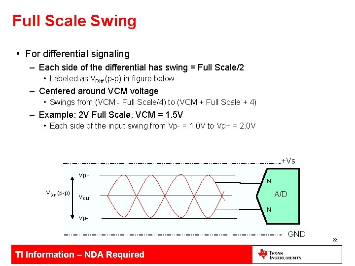
Full Scale Swing • For differential signaling – Each side of the differential has swing = Full Scale/2 • Labeled as VDiff (p-p) in figure below – Centered around VCM voltage • Swings from (VCM - Full Scale/4) to (VCM + Full Scale + 4) – Example: 2 V Full Scale, VCM = 1. 5 V • Each side of the input swing from Vp- = 1. 0 V to Vp+ = 2. 0 V +Vs Vp+ VDiff (p-p) IN A/D VCM IN Vp- GND TI Information – NDA Required 22

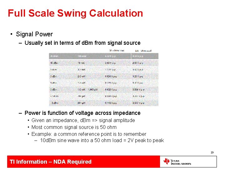
Full Scale Swing Calculation • Signal Power – Usually set in terms of d. Bm from signal source – Power is function of voltage across impedance • Given an impedance, d. Bm => signal amplitude • Most common signal source is 50 ohm • Example: a common reference point is to remember – 10 d. Bm sine wave into a 50 ohm load = 2 V peak to peak 23 TI Information – NDA Required

ADC Common Mode (VCM) • ADCs have an internally generated common mode, however it can be set externally • Internally generated common mode of the ADC can be used as an output to source the common mode of a driving amplifier – Sometimes the VREF can be used as the VCM – but be careful – they are not always the same voltage • VCM can be forced from an external common mode (ex. amplifier) – Follow the datasheet recommendation for range. External VCM range can vary between ADCs. Ex. ADS 6149 VCM =1. 5 V +/-100 m. V – Using external VCM can reduce the dynamic range and headroom. 24 TI Information – NDA Required

Oversampling, Undersampling & Aliasing 25 TI Information – NDA Required

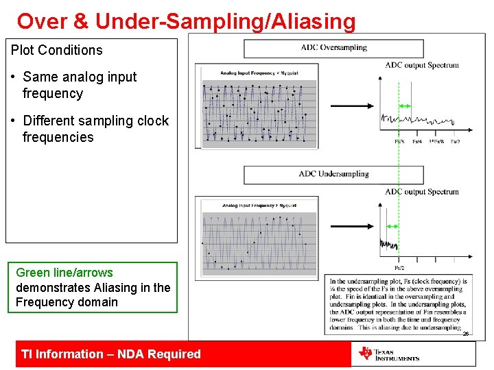
Over & Under-Sampling/Aliasing Plot Conditions • Same analog input frequency • Different sampling clock frequencies Green line/arrows demonstrates Aliasing in the Frequency domain 26 TI Information – NDA Required

Importance of Aliasing • Aliasing does have useful properties • As shown on the previous slide Aliasing can be used to down convert a signal to a lower frequency. • By designing ADCs that can undersample IF frequencies, we can down convert them to Baseband Frequencies. • This allows our customers to avoid the cost of an extra analog mixer to down convert the frequency 27 TI Information – NDA Required

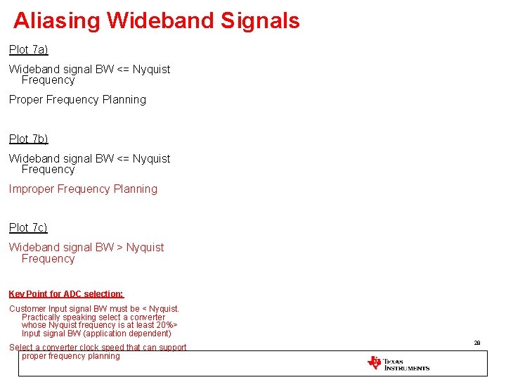
Aliasing Wideband Signals Plot 7 a) Wideband signal BW <= Nyquist Frequency Proper Frequency Planning Plot 7 b) Wideband signal BW <= Nyquist Frequency Improper Frequency Planning Plot 7 c) Wideband signal BW > Nyquist Frequency Key Point for ADC selection: Customer Input signal BW must be < Nyquist. Practically speaking select a converter whose Nyquist frequency is at least 20%> Input signal BW (application dependent) Select a converter clock speed that can support proper frequency planning 28

Clocking High Speed ADCs 29 TI Information – NDA Required

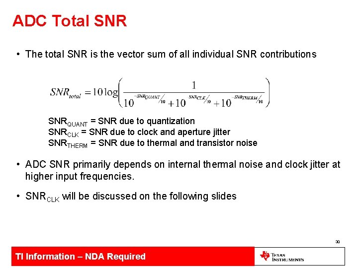
ADC Total SNR • The total SNR is the vector sum of all individual SNR contributions SNRQUANT = SNR due to quantization SNRCLK = SNR due to clock and aperture jitter SNRTHERM = SNR due to thermal and transistor noise • ADC SNR primarily depends on internal thermal noise and clock jitter at higher input frequencies. • SNRCLK will be discussed on the following slides 30 TI Information – NDA Required

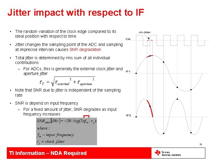
Jitter impact with respect to IF • The random variation of the clock edge compared to its ideal position with respect to time • Jitter changes the sampling point of the ADC and sampling at imprecise intervals causes SNR degradation • Total jitter is determined by rms sum of all individual contributions – For ADCs, this is generally the external clock jitter and aperture jitter • Note that SNR due to jitter is independent of the sampling rate • SNR is depend on input frequency – For a fixed amount of jitter, SNR degrades as input frequency increases 31 TI Information – NDA Required

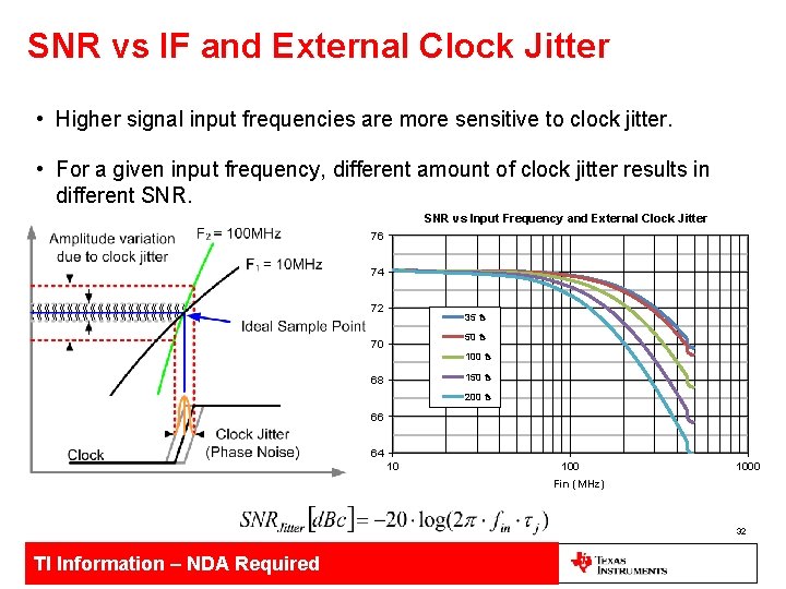
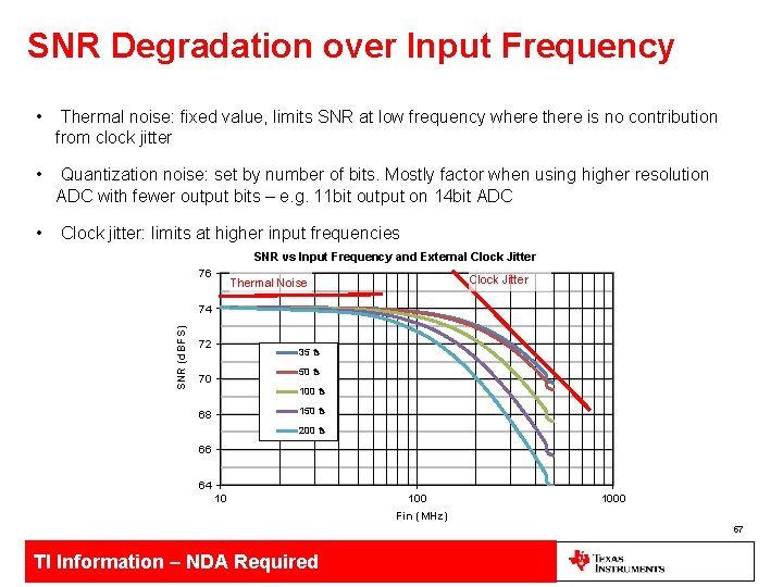
SNR vs IF and External Clock Jitter • Higher signal input frequencies are more sensitive to clock jitter. • For a given input frequency, different amount of clock jitter results in different SNR vs Input Frequency and External Clock Jitter 76 SNR (d. BFS) 74 72 35 fs 50 fs 70 100 fs 150 fs 68 200 fs 66 64 10 1000 Fin (MHz) 32 TI Information – NDA Required

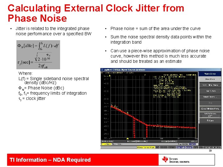
Calculating External Clock Jitter from Phase Noise • Jitter is related to the integrated phase noise performance over a specified BW • Phase noise = sum of the area under the curve • Sum the noise spectral density data points within the integration band • Can use a piece-wise approximation of phase noise curve, however this method is much less accurate and should be treated as an estimate Where: L(f) = Single sideband noise spectral density (d. Bc/Hz) FN= Phase Noise (d. Bc) f 0, f 1= frequency limits of integration tj = clock jitter 33 TI Information – NDA Required

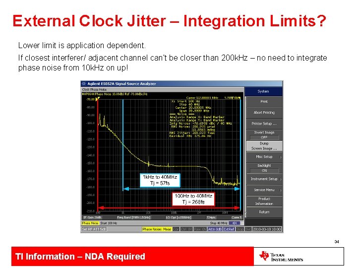
External Clock Jitter – Integration Limits? Lower limit is application dependent. If closest interferer/ adjacent channel can’t be closer than 200 k. Hz – no need to integrate phase noise from 10 k. Hz on up! 34 TI Information – NDA Required

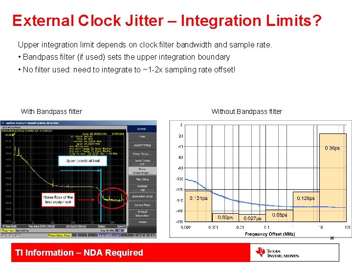
External Clock Jitter – Integration Limits? Upper integration limit depends on clock filter bandwidth and sample rate. • Bandpass filter (if used) sets the upper integration boundary • No filter used: need to integrate to ~1 -2 x sampling rate offset! With Bandpass filter Without Bandpass filter 35 TI Information – NDA Required

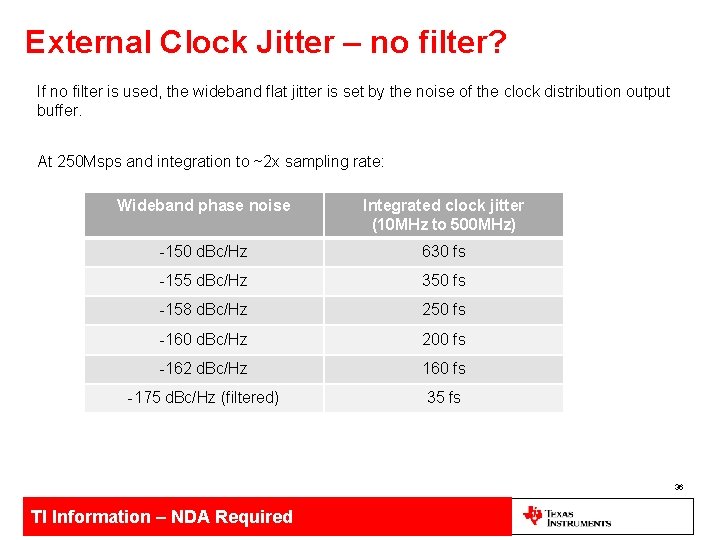
External Clock Jitter – no filter? If no filter is used, the wideband flat jitter is set by the noise of the clock distribution output buffer. At 250 Msps and integration to ~2 x sampling rate: Wideband phase noise Integrated clock jitter (10 MHz to 500 MHz) -150 d. Bc/Hz 630 fs -155 d. Bc/Hz 350 fs -158 d. Bc/Hz 250 fs -160 d. Bc/Hz 200 fs -162 d. Bc/Hz 160 fs -175 d. Bc/Hz (filtered) 35 fs 36 TI Information – NDA Required

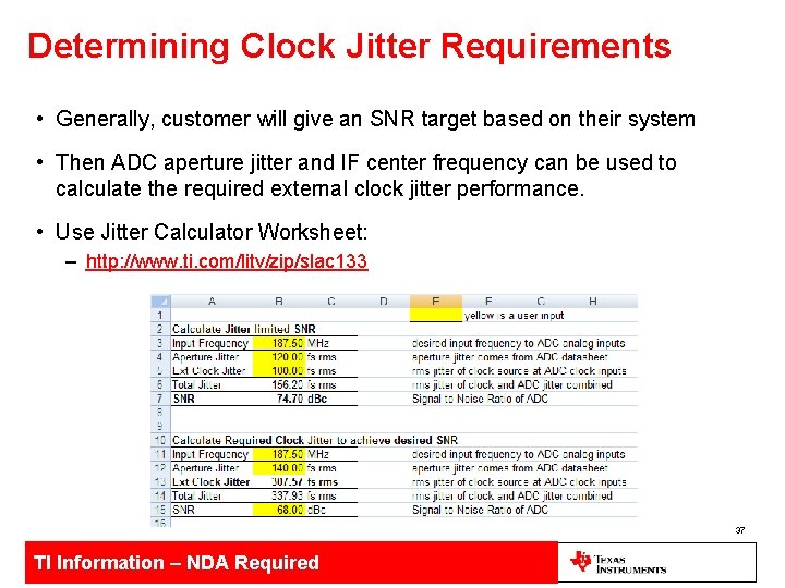
Determining Clock Jitter Requirements • Generally, customer will give an SNR target based on their system • Then ADC aperture jitter and IF center frequency can be used to calculate the required external clock jitter performance. • Use Jitter Calculator Worksheet: – http: //www. ti. com/litv/zip/slac 133 37 TI Information – NDA Required

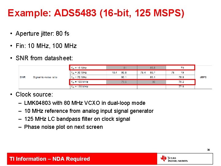
Example: ADS 5483 (16 -bit, 125 MSPS) • Aperture jitter: 80 fs • Fin: 10 MHz, 100 MHz • SNR from datasheet: • Clock source: – – LMK 04803 with 80 MHz VCXO in dual-loop mode 10 MHz reference from analog input signal generator 125 MHz LC bandpass filter on clock signal Phase noise plot on next screen 38 TI Information – NDA Required

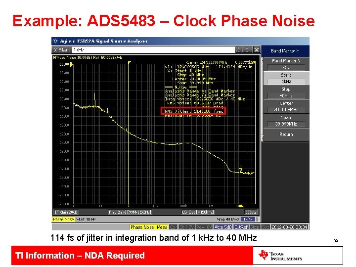
Example: ADS 5483 – Clock Phase Noise 114 fs of jitter in integration band of 1 k. Hz to 40 MHz TI Information – NDA Required 39

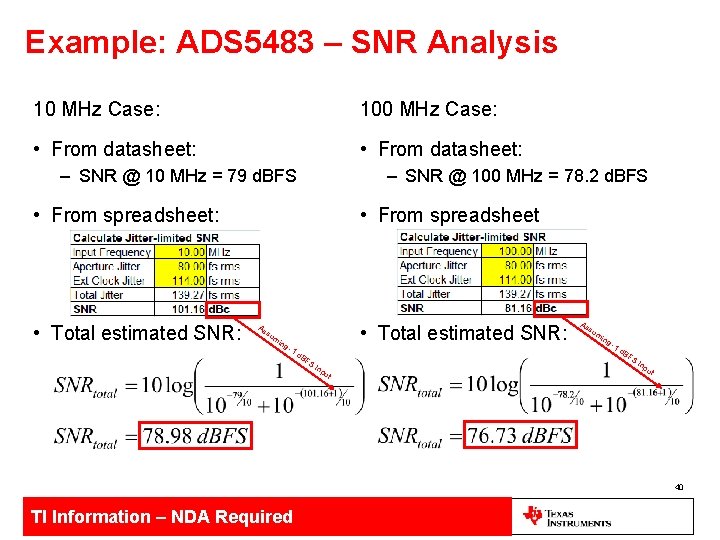
Example: ADS 5483 – SNR Analysis 10 MHz Case: 100 MHz Case: • From datasheet: – SNR @ 10 MHz = 79 d. BFS – SNR @ 100 MHz = 78. 2 d. BFS • From spreadsheet: • Total estimated SNR: • From spreadsheet As su mi ng -1 • Total estimated SNR: d. B FS Inp As su mi ng -1 d. B FS ut Inp ut 40 TI Information – NDA Required

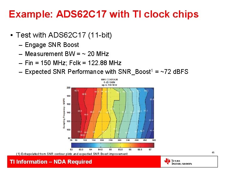
Example: ADS 62 C 17 with TI clock chips • Test with ADS 62 C 17 (11 -bit) – – Engage SNR Boost Measurement BW = ~ 20 MHz Fin = 150 MHz; Fclk = 122. 88 MHz Expected SNR Performance with SNR_Boost 1 = ~72 d. BFS (1) Extrapolated from SNR contour plots and expected SNR Boost improvement TI Information – NDA Required 41

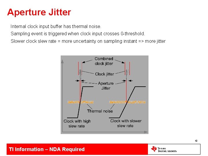
Aperture Jitter Internal clock input buffer has thermal noise. Sampling event is triggered when clock input crosses 0 -threshold. Slower clock slew rate = more uncertainty on sampling instant => more jitter 42 TI Information – NDA Required

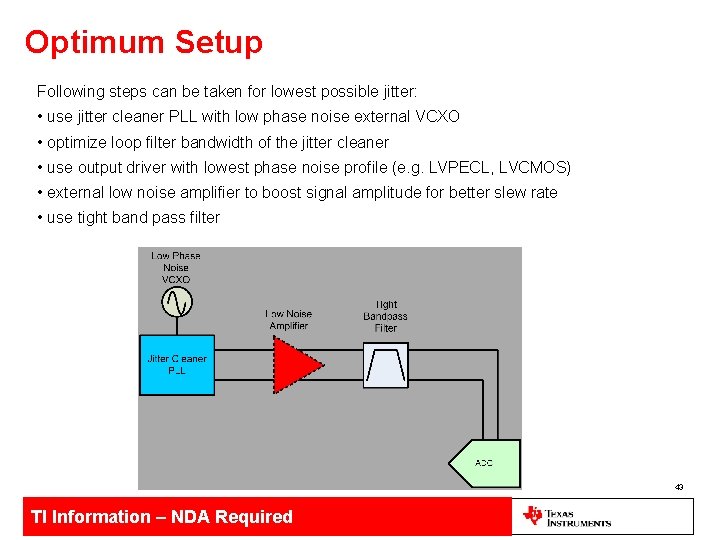
Optimum Setup Following steps can be taken for lowest possible jitter: • use jitter cleaner PLL with low phase noise external VCXO • optimize loop filter bandwidth of the jitter cleaner • use output driver with lowest phase noise profile (e. g. LVPECL, LVCMOS) • external low noise amplifier to boost signal amplitude for better slew rate • use tight band pass filter 43 TI Information – NDA Required

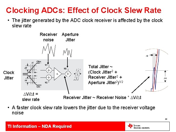
Clocking ADCs: Effect of Clock Slew Rate • The jitter generated by the ADC clock receiver is affected by the clock slew rate Receiver noise Aperture Jitter Total Jitter ~ (Clock Jitter 2 + Receiver Jitter 2 + Aperture Jitter 2)1/2 Clock Jitter DV/Dt = slew rate Receiver Jitter ~ Receiver Noise * DV/Dt • A faster clock slew rate lowers the jitter due to the receiver voltage noise 44 TI Information – NDA Required

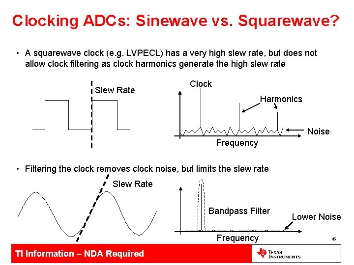
Clocking ADCs: Sinewave vs. Squarewave? • A squarewave clock (e. g. LVPECL) has a very high slew rate, but does not allow clock filtering as clock harmonics generate the high slew rate Slew Rate Clock Harmonics Noise Frequency • Filtering the clock removes clock noise, but limits the slew rate Slew Rate Bandpass Filter Frequency TI Information – NDA Required Lower Noise 45

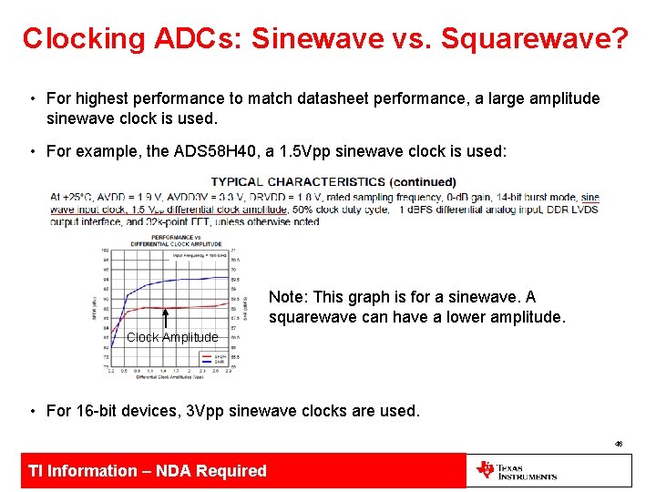
Clocking ADCs: Sinewave vs. Squarewave? • For highest performance to match datasheet performance, a large amplitude sinewave clock is used. • For example, the ADS 58 H 40, a 1. 5 Vpp sinewave clock is used: Note: This graph is for a sinewave. A squarewave can have a lower amplitude. Clock Amplitude • For 16 -bit devices, 3 Vpp sinewave clocks are used. 46 TI Information – NDA Required

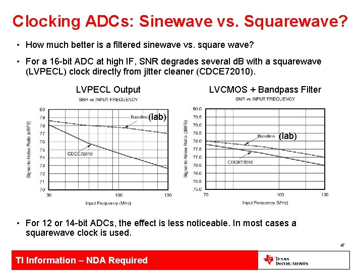
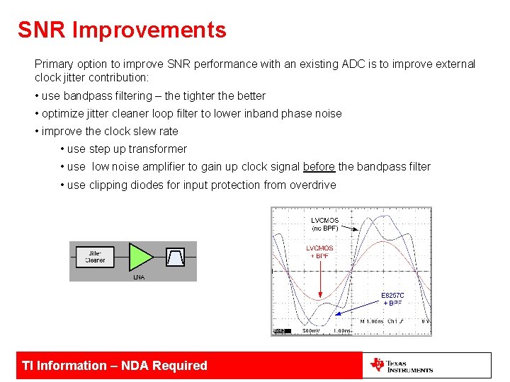
Clocking ADCs: Sinewave vs. Squarewave? • How much better is a filtered sinewave vs. square wave? • For a 16 -bit ADC at high IF, SNR degrades several d. B with a squarewave (LVPECL) clock directly from jitter cleaner (CDCE 72010). LVCMOS + Bandpass Filter LVPECL Output (lab) • For 12 or 14 -bit ADCs, the effect is less noticeable. In most cases a squarewave clock is used. 47 TI Information – NDA Required

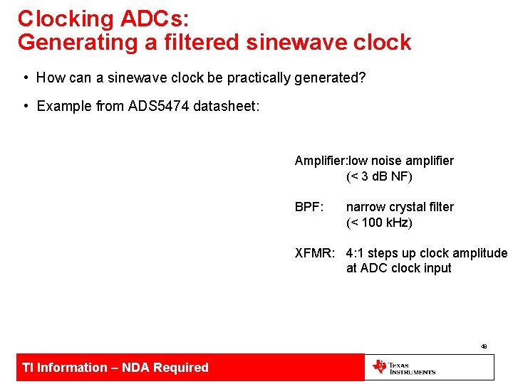
Clocking ADCs: Generating a filtered sinewave clock • How can a sinewave clock be practically generated? • Example from ADS 5474 datasheet: Amplifier: low noise amplifier (< 3 d. B NF) BPF: narrow crystal filter (< 100 k. Hz) XFMR: 4: 1 steps up clock amplitude at ADC clock input 48 TI Information – NDA Required

A Note on Clock Filtering • Clock sources have wideband noise that will also contribute to the overall jitter of the clock • In order to eliminate the wideband noise, a filter needs to be placed on the clock lines • The amount of filtering may vary based on the system, but a simple LC tank circuit may be enough • Note that filtering a square wave will produce a sine wave with a slower slew rate, this may hurt the jitter performance slightly, but the gain from eliminated wideband noise will offset this • Clocking with a filtered sine wave may also reduce clock related spurs 49 TI Information – NDA Required

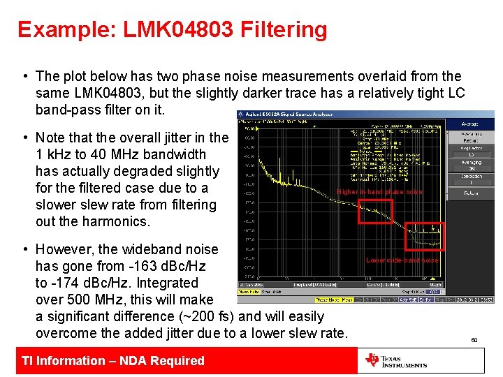
Example: LMK 04803 Filtering • The plot below has two phase noise measurements overlaid from the same LMK 04803, but the slightly darker trace has a relatively tight LC band-pass filter on it. • Note that the overall jitter in the 1 k. Hz to 40 MHz bandwidth has actually degraded slightly for the filtered case due to a slower slew rate from filtering out the harmonics. Higher in-band phase noise • However, the wideband noise has gone from -163 d. Bc/Hz to -174 d. Bc/Hz. Integrated over 500 MHz, this will make a significant difference (~200 fs) and will easily overcome the added jitter due to a lower slew rate. TI Information – NDA Required Lower wide-band noise 50

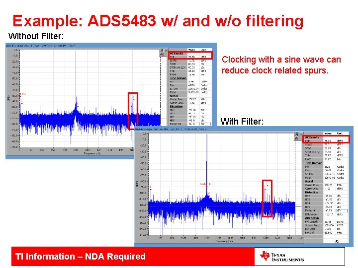
Example: ADS 5483 w/ and w/o filtering Without Filter: Clocking with a sine wave can reduce clock related spurs. With Filter: 51 TI Information – NDA Required

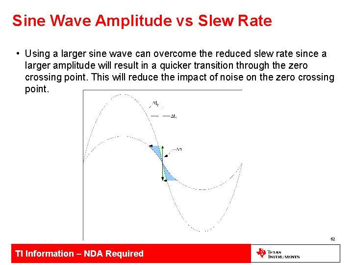
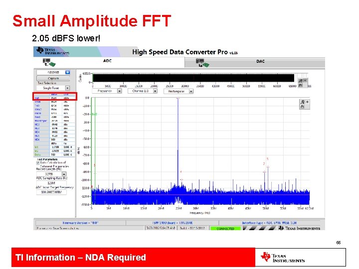
Sine Wave Amplitude vs Slew Rate • Using a larger sine wave can overcome the reduced slew rate since a larger amplitude will result in a quicker transition through the zero crossing point. This will reduce the impact of noise on the zero crossing point. 52 TI Information – NDA Required

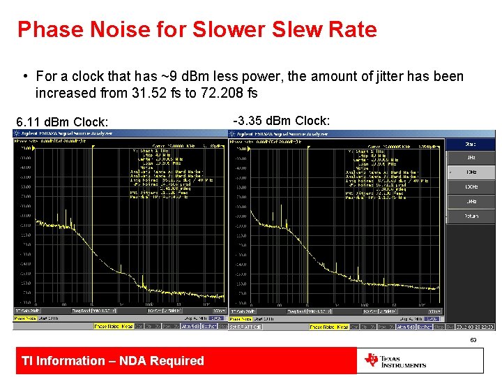
Phase Noise for Slower Slew Rate • For a clock that has ~9 d. Bm less power, the amount of jitter has been increased from 31. 52 fs to 72. 208 fs 6. 11 d. Bm Clock: -3. 35 d. Bm Clock: 53 TI Information – NDA Required

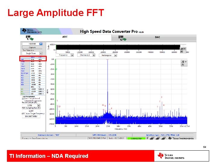
Large Amplitude FFT 54 TI Information – NDA Required

Small Amplitude FFT 2. 05 d. BFS lower! 55 TI Information – NDA Required

SNR&SFDR Degradation over Input Frequency 56 TI Information – NDA Required

SNR Degradation over Input Frequency • Thermal noise: fixed value, limits SNR at low frequency where there is no contribution from clock jitter • Quantization noise: set by number of bits. Mostly factor when using higher resolution ADC with fewer output bits – e. g. 11 bit output on 14 bit ADC • Clock jitter: limits at higher input frequencies SNR vs Input Frequency and External Clock Jitter 76 Clock Jitter Thermal Noise SNR (d. BFS) 74 72 35 fs 50 fs 70 100 fs 150 fs 68 200 fs 66 64 10 1000 Fin (MHz) 57 TI Information – NDA Required

SFDR Degradation over Input Frequency • Buffer performance degrades over input frequency • Sampling network degrades over input frequency • Internal matching is harder to do for higher frequencies 58 TI Information – NDA Required

Improving ADC SNR & SFDR 59 TI Information – NDA Required

SNR Improvements Primary option to improve SNR performance with an existing ADC is to improve external clock jitter contribution: • use bandpass filtering – the tighter the better • optimize jitter cleaner loop filter to lower inband phase noise • improve the clock slew rate • use step up transformer • use low noise amplifier to gain up clock signal before the bandpass filter • use clipping diodes for input protection from overdrive TI Information – NDA Required

SFDR Improvements • Use buffered inputs for better HD 2, 3 performance • Trade off SNR for better SFDR performance using digital gain feature – lower input amplitude helps improve HD 2, 3 • Minimize differential mismatch within differential pair – common mode mismatch (phase and amplitude) cause HD 2 degradation – improve component tolerance to reduce mismatch • Dither TI Information – NDA Required

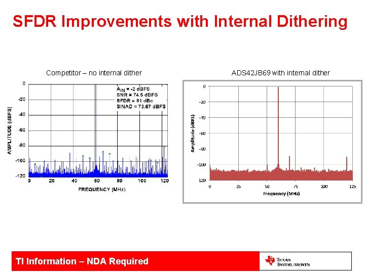
Dither in an ADC • An ADC will have deterministic and systematic errors that repeat each time those codes are exercised • Dither (low level noise) can randomize those errors such that they are minimized • The harmonics are still present, but at lower levels • Dither can have the adverse affect of increasing the overall noise floor – acceptable for some applications • Some Dither techniques add the noise in areas of the circuit that need to be randomized and then attempt to subtract the noise later so that the degradation in SNR is minimized or not even noticeable by the user • It is a technique used to improve the ADC’s distortion beyond its inherent linearity 62 TI Information – NDA Required

SFDR Improvements with Internal Dithering Competitor – no internal dither TI Information – NDA Required ADS 42 JB 69 with internal dither

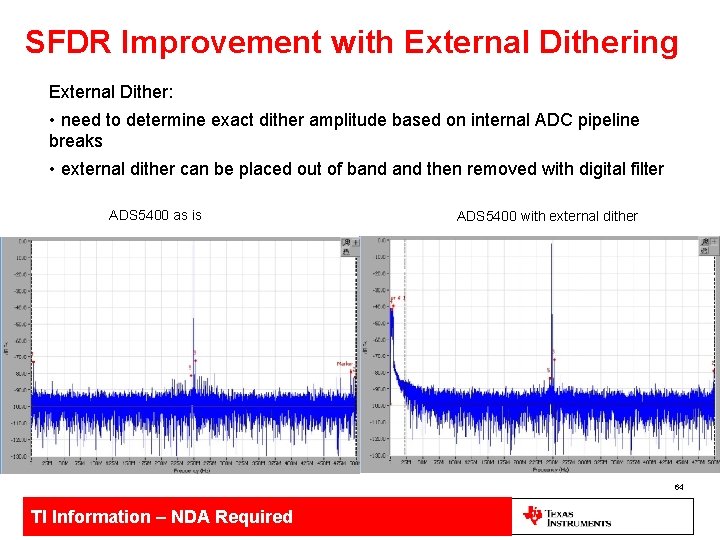
SFDR Improvement with External Dithering External Dither: • need to determine exact dither amplitude based on internal ADC pipeline breaks • external dither can be placed out of band then removed with digital filter ADS 5400 as is ADS 5400 with external dither 64 TI Information – NDA Required

Thank you! 65 TI Information – NDA Required