DAC Concepts Texas Instruments High Speed Data Converters
- Slides: 57

DAC Concepts Texas Instruments High Speed Data Converters June 2014 1

Outline • Current steering architecture used in high speed DACs – what is inside • DAC full-scale calculation • DAC specifications – SNR, SFDR, IMD – Harmonics in sampled systems • Noise and distortion in high speed DACs • Clocking high speed DACs – phase noise, jitter, slew rate • Improving DAC SFDR with dithering 2 TI Information – NDA Required

High Speed Current Steering DACs - what is inside 3 TI Information – NDA Required

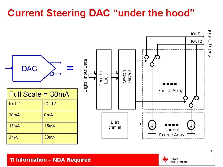
IOUT 1 Full Scale = 30 m. A IOUT 1 IOUT 2 30 m. A 15 m. A 0 m. A 30 m. A Switch Drivers Decoder Logic = DAC Digital Input Data IOUT 2 Analog Output Current Steering DAC “under the hood” Switch Array Bias Circuit Current Source Array 4 TI Information – NDA Required

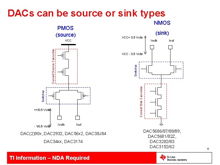
DACs can be source or sink types NMOS PMOS (source) VCC+ 0. 5 Volts Current Source Cascodes VCC Ioutb Iout Switches Current Sink Cascodes Switches VCC - 0. 5 Volts +1/0. 5 Volts - 1/0. 5 Volts (sink) Ioutb Iout DAC(2)90 x, DAC 2932, DAC 56 x 2, DAC 38 J 84 DAC 34 xx, DAC 3174 TI Information – NDA Required DAC 5686/87/88/89, DAC 5681/82 Z, DAC 3282/83 DAC 3152/62 5

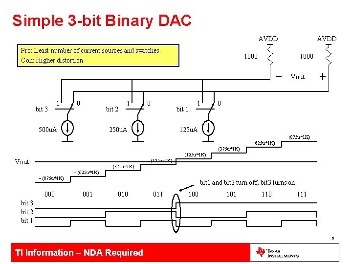
Simple 3 -bit Binary DAC AVDD Pro: Least number of current sources and switches. Con: Higher distortion. AVDD 1000 Vout bit 3 1 0 bit 2 500 u. A 1 0 bit 1 250 u. A 1 0 125 u. A (875 u*1 K) (625 u*1 K) (375 u*1 K) (125 u*1 K) – (125 u*1 K) Vout – (375 u*1 K) – (625 u*1 K) – (875 u*1 K) 000 bit 1 and bit 2 turn off, bit 3 turns on 001 010 011 100 101 110 111 bit 3 bit 2 bit 1 6 TI Information – NDA Required

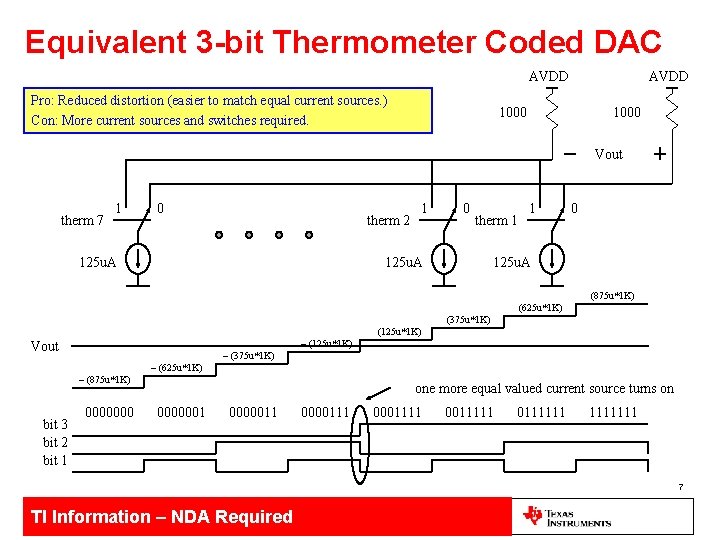
Equivalent 3 -bit Thermometer Coded DAC AVDD Pro: Reduced distortion (easier to match equal current sources. ) Con: More current sources and switches required. AVDD 1000 Vout therm 7 1 0 therm 2 125 u. A 1 0 therm 1 125 u. A 1 0 125 u. A (875 u*1 K) (625 u*1 K) (375 u*1 K) (125 u*1 K) – (125 u*1 K) Vout – (375 u*1 K) – (625 u*1 K) – (875 u*1 K) bit 3 bit 2 bit 1 0000000 one more equal valued current source turns on 00000011 00001111 00111111 1111111 7 TI Information – NDA Required

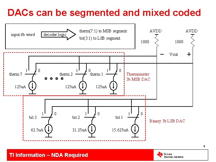
DACs can be segmented and mixed coded input 6 b word therm(7: 1) to MSB segment decoder logic AVDD bit(3: 1) to LSB segment 1000 AVDD 1000 Vout therm 7 1 0 therm 2 125 u. A 1 0 1 therm 1 125 u. A bit 3 1 62. 5 u. A 0 bit 2 0 Thermometer 3 b MSB DAC 125 u. A 1 31. 25 u. A 0 bit 1 1 0 Binary 3 b LSB DAC 15. 625 u. A 8 TI Information – NDA Required

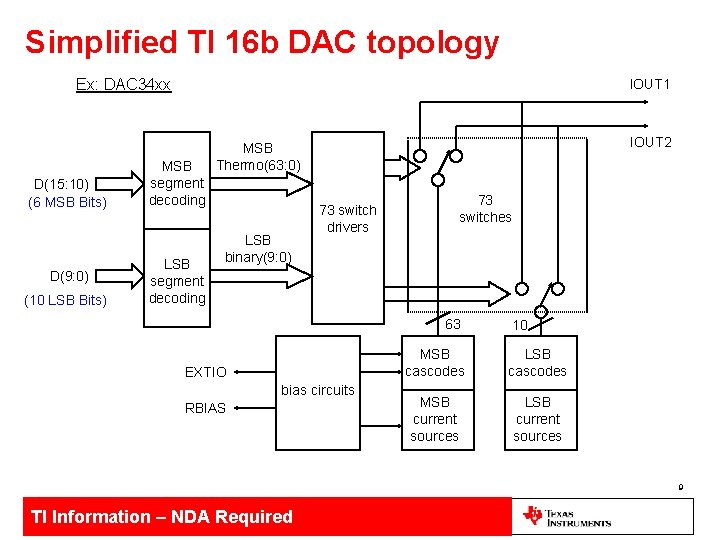
Simplified TI 16 b DAC topology Ex: DAC 34 xx D(15: 10) (6 MSB Bits) D(9: 0) (10 LSB Bits) IOUT 1 MSB segment decoding LSB segment decoding IOUT 2 MSB Thermo(63: 0) LSB binary(9: 0) 73 switch drivers 73 switches 63 EXTIO bias circuits RBIAS 10 MSB cascodes LSB cascodes MSB current sources LSB current sources 9 TI Information – NDA Required

DAC Full-scale Calculation 10 TI Information – NDA Required

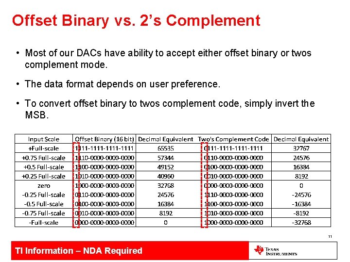
Offset Binary vs. 2’s Complement • Most of our DACs have ability to accept either offset binary or twos complement mode. • The data format depends on user preference. • To convert offset binary to twos complement code, simply invert the MSB. 11 TI Information – NDA Required

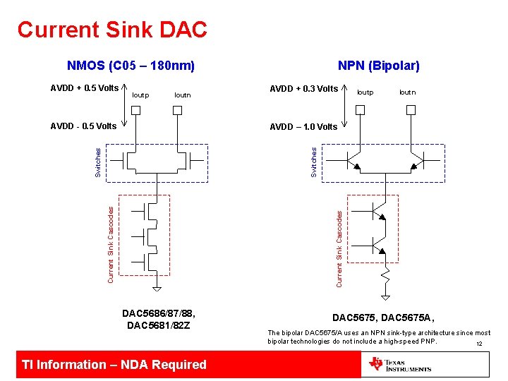
Current Sink DAC NMOS (C 05 – 180 nm) AVDD + 0. 5 Volts Ioutp Ioutn AVDD - 0. 5 Volts NPN (Bipolar) AVDD + 0. 3 Volts Ioutp Ioutn Current Sink Cascodes Switches AVDD – 1. 0 Volts DAC 5686/87/88, DAC 5681/82 Z TI Information – NDA Required DAC 5675, DAC 5675 A, The bipolar DAC 5675/A uses an NPN sink-type architecture since most bipolar technologies do not include a high-speed PNP. 12

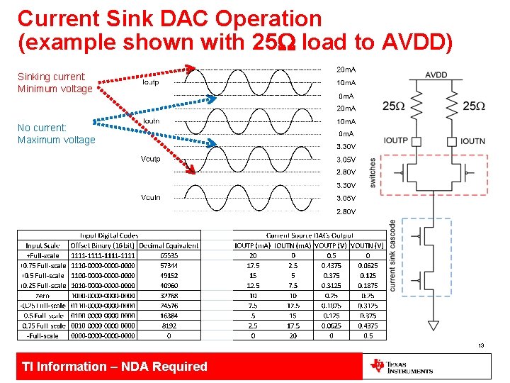
Current Sink DAC Operation (example shown with 25 W load to AVDD) Sinking current: Minimum voltage No current: Maximum voltage 13 TI Information – NDA Required

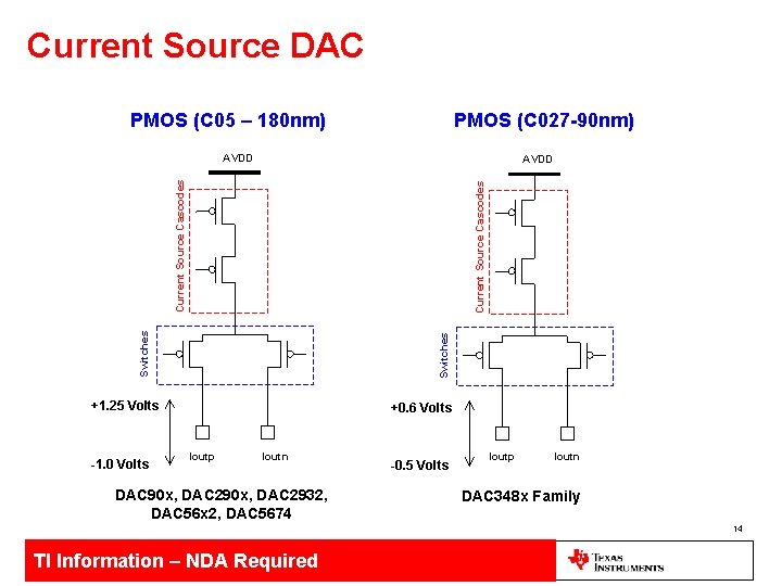
Current Source DAC PMOS (C 05 – 180 nm) PMOS (C 027 -90 nm) AVDD Switches Current Source Cascodes AVDD +1. 25 Volts -1. 0 Volts +0. 6 Volts Ioutp Ioutn DAC 90 x, DAC 2932, DAC 56 x 2, DAC 5674 -0. 5 Volts Ioutp Ioutn DAC 348 x Family 14 TI Information – NDA Required

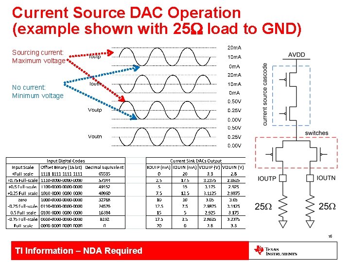
Current Source DAC Operation (example shown with 25 W load to GND) Sourcing current: Maximum voltage No current: Minimum voltage 15 TI Information – NDA Required

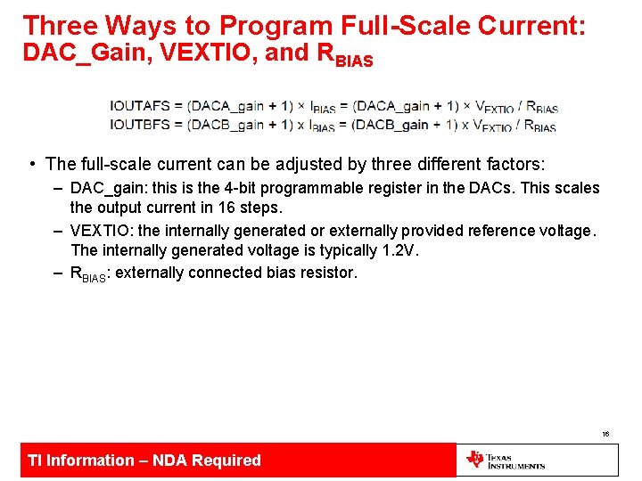
Three Ways to Program Full-Scale Current: DAC_Gain, VEXTIO, and RBIAS • The full-scale current can be adjusted by three different factors: – DAC_gain: this is the 4 -bit programmable register in the DACs. This scales the output current in 16 steps. – VEXTIO: the internally generated or externally provided reference voltage. The internally generated voltage is typically 1. 2 V. – RBIAS: externally connected bias resistor. 16 TI Information – NDA Required

DAC Specifications 17 TI Information – NDA Required

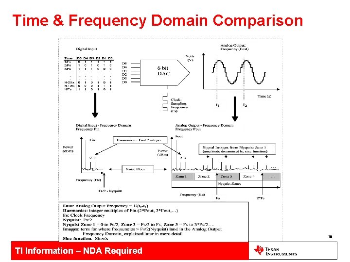
Time & Frequency Domain Comparison 18 TI Information – NDA Required

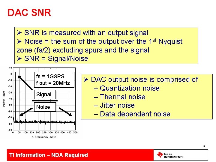
DAC SNR Ø SNR is measured with an output signal Ø Noise = the sum of the output over the 1 st Nyquist zone (fs/2) excluding spurs and the signal Ø SNR = Signal/Noise fs = 1 GSPS f out = 20 MHz Signal Noise Ø DAC output noise is comprised of – Quantization noise – Thermal noise – Jitter noise – Data dependent noise 19 TI Information – NDA Required

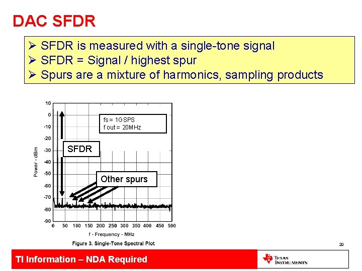
DAC SFDR Ø SFDR is measured with a single-tone signal Ø SFDR = Signal / highest spur Ø Spurs are a mixture of harmonics, sampling products fs = 1 GSPS f out = 20 MHz SFDR Other spurs 20 TI Information – NDA Required

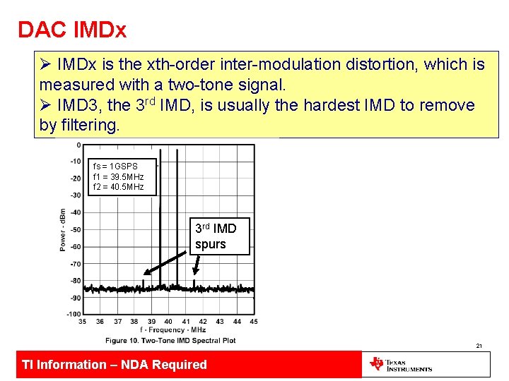
DAC IMDx Ø IMDx is the xth-order inter-modulation distortion, which is measured with a two-tone signal. Ø IMD 3, the 3 rd IMD, is usually the hardest IMD to remove by filtering. fs = 1 GSPS f 1 = 39. 5 MHz f 2 = 40. 5 MHz 3 rd IMD spurs 21 TI Information – NDA Required

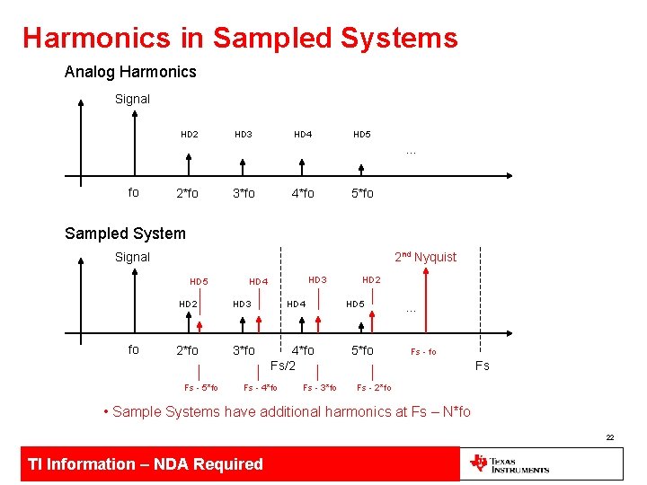
Harmonics in Sampled Systems Analog Harmonics Signal HD 2 HD 3 HD 4 HD 5 … fo 2*fo 3*fo 4*fo 5*fo Sampled System Signal 2 nd Nyquist HD 5 fo HD 2 HD 3 2*fo 3*fo Fs - 5*fo HD 3 HD 4 4*fo Fs/2 Fs - 4*fo Fs - 3*fo HD 2 HD 5 5*fo … Fs - fo Fs Fs - 2*fo • Sample Systems have additional harmonics at Fs – N*fo 22 TI Information – NDA Required

Noise and Distortion in High Speed DACs 23 TI Information – NDA Required

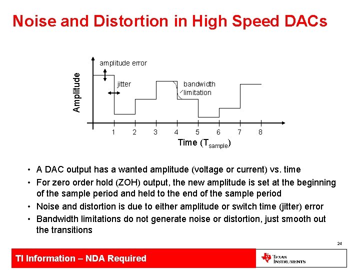
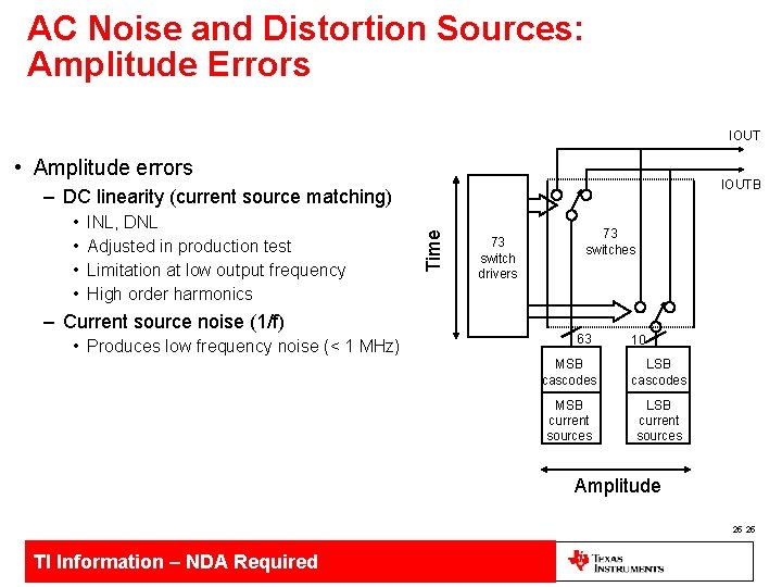
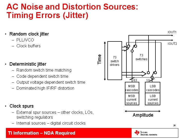
Noise and Distortion in High Speed DACs Amplitude amplitude error jitter 1 bandwidth limitation 2 3 4 5 6 7 8 Time (Tsample) • A DAC output has a wanted amplitude (voltage or current) vs. time • For zero order hold (ZOH) output, the new amplitude is set at the beginning of the sample period and held to the end of the sample period • Noise and distortion is due to either amplitude or switch time (jitter) error • Bandwidth limitations do not generate noise or distortion, just smooth out the transitions 24 TI Information – NDA Required

AC Noise and Distortion Sources: Amplitude Errors IOUT • Amplitude errors IOUTB • • INL, DNL Adjusted in production test Limitation at low output frequency High order harmonics – Current source noise (1/f) • Produces low frequency noise (< 1 MHz) Time – DC linearity (current source matching) 73 switch drivers 73 switches 63 10 MSB cascodes LSB cascodes MSB current sources LSB current sources Amplitude 25 25 TI Information – NDA Required

AC Noise and Distortion Sources: Timing Errors (Jitter) IOUT 1 • Random clock jitter – PLL/VCO – Clock buffers – – Random switch time matching Code dependent switch time Output voltage dependent switch time Dominated high IF/RF distortion • Clock spurs – External spur sources – other clocks, LOs, switching regulators – Internal sources – digital circuit clocks TI Information – NDA Required Time • Deterministic jitter IOUT 2 73 switch drivers 73 switches 63 10 MSB cascodes LSB cascodes MSB current sources LSB current sources Amplitude 26

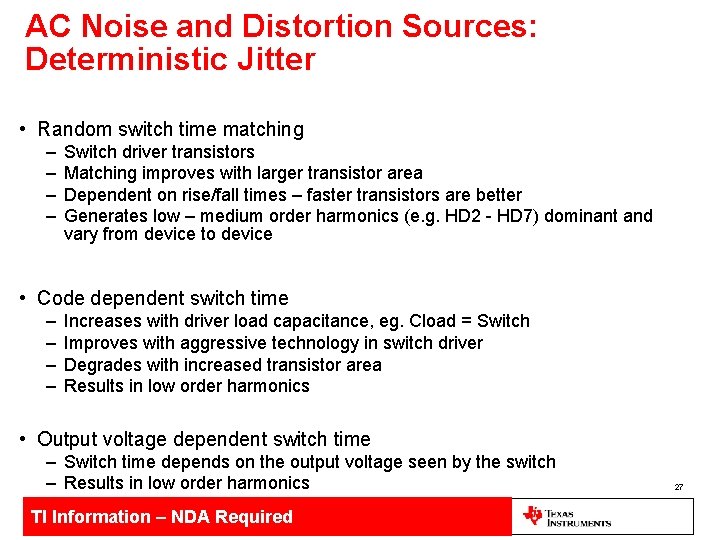
AC Noise and Distortion Sources: Deterministic Jitter • Random switch time matching – – Switch driver transistors Matching improves with larger transistor area Dependent on rise/fall times – faster transistors are better Generates low – medium order harmonics (e. g. HD 2 - HD 7) dominant and vary from device to device • Code dependent switch time – – Increases with driver load capacitance, eg. Cload = Switch Improves with aggressive technology in switch driver Degrades with increased transistor area Results in low order harmonics • Output voltage dependent switch time – Switch time depends on the output voltage seen by the switch – Results in low order harmonics TI Information – NDA Required 27

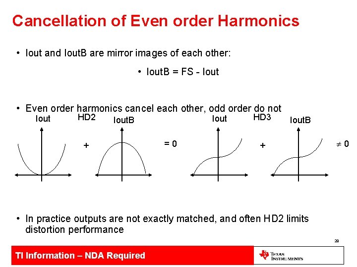
Cancellation of Even order Harmonics • Iout and Iout. B are mirror images of each other: • Iout. B = FS - Iout • Even order harmonics cancel each other, odd order do not Iout HD 2 Iout. B + =0 HD 3 Iout. B + ¹ 0 • In practice outputs are not exactly matched, and often HD 2 limits distortion performance 28 TI Information – NDA Required

Clocking High Speed DACs 29 TI Information – NDA Required

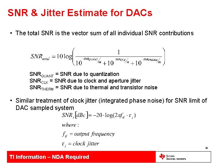
SNR & Jitter Estimate for DACs • The total SNR is the vector sum of all individual SNR contributions SNRQUANT = SNR due to quantization SNRCLK = SNR due to clock and aperture jitter SNRTHERM = SNR due to thermal and transistor noise • Similar treatment of clock jitter (integrated phase noise) for SNR limit of DAC sampled system 30 TI Information – NDA Required

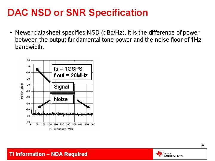
DAC NSD or SNR Specification • Newer datasheet specifies NSD (d. Bc/Hz). It is the difference of power between the output fundamental tone power and the noise floor of 1 Hz bandwidth. fs = 1 GSPS f out = 20 MHz Signal Noise 31 TI Information – NDA Required

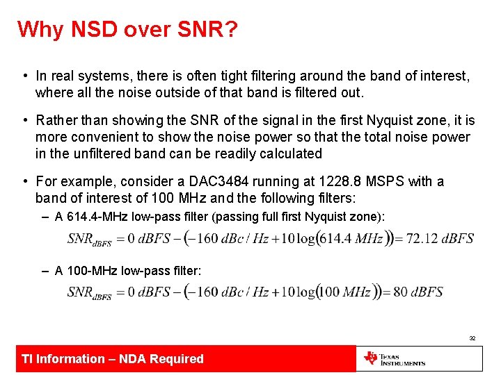
Why NSD over SNR? • In real systems, there is often tight filtering around the band of interest, where all the noise outside of that band is filtered out. • Rather than showing the SNR of the signal in the first Nyquist zone, it is more convenient to show the noise power so that the total noise power in the unfiltered band can be readily calculated • For example, consider a DAC 3484 running at 1228. 8 MSPS with a band of interest of 100 MHz and the following filters: – A 614. 4 -MHz low-pass filter (passing full first Nyquist zone): – A 100 -MHz low-pass filter: 32 TI Information – NDA Required

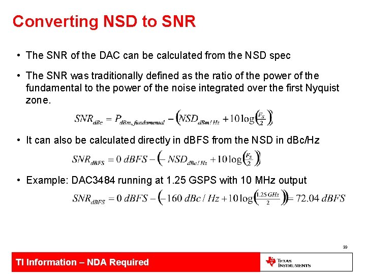
Converting NSD to SNR • The SNR of the DAC can be calculated from the NSD spec • The SNR was traditionally defined as the ratio of the power of the fundamental to the power of the noise integrated over the first Nyquist zone. • It can also be calculated directly in d. BFS from the NSD in d. Bc/Hz • Example: DAC 3484 running at 1. 25 GSPS with 10 MHz output 33 TI Information – NDA Required

NSD to SNR tradeoffs – Jitter/Phase noise • SNR estimates based on Jitter are good estimates for SNR for the entire Nyquist band – may be too pessimistic for BW limited applications. • SNR estimates based on NSD (typically measured at some MHz offset) do not account for close-in phase noise which could affect inband EVM - would be good for out of band estimates like ACPR • Using the clock NSD and BW limited noise calculations would be the ideal solution for in-band out-of-band measurements. 34 TI Information – NDA Required

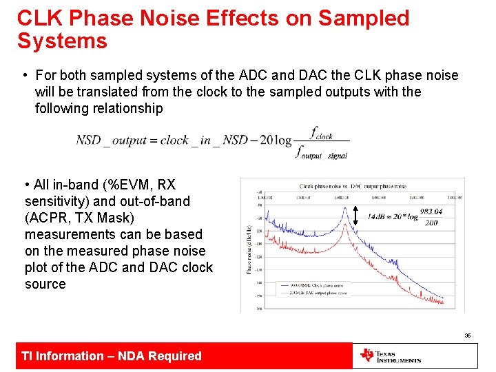
CLK Phase Noise Effects on Sampled Systems • For both sampled systems of the ADC and DAC the CLK phase noise will be translated from the clock to the sampled outputs with the following relationship • All in-band (%EVM, RX sensitivity) and out-of-band (ACPR, TX Mask) measurements can be based on the measured phase noise plot of the ADC and DAC clock source 35 TI Information – NDA Required

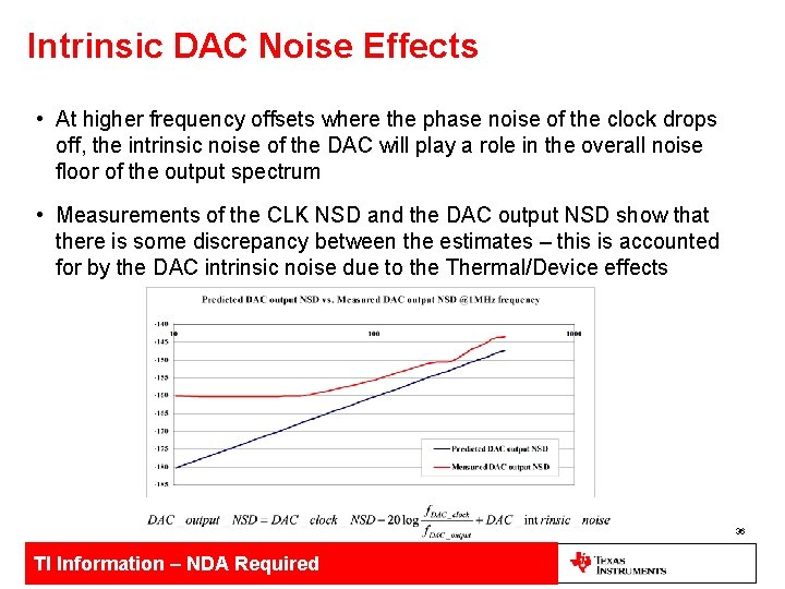
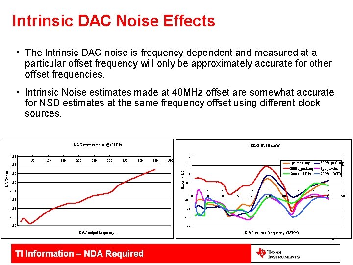
Intrinsic DAC Noise Effects • At higher frequency offsets where the phase noise of the clock drops off, the intrinsic noise of the DAC will play a role in the overall noise floor of the output spectrum • Measurements of the CLK NSD and the DAC output NSD show that there is some discrepancy between the estimates – this is accounted for by the DAC intrinsic noise due to the Thermal/Device effects 36 TI Information – NDA Required

Intrinsic DAC Noise Effects • The Intrinsic DAC noise is frequency dependent and measured at a particular offset frequency will only be approximately accurate for other offset frequencies. • Intrinsic Noise estimates made at 40 MHz offset are somewhat accurate for NSD estimates at the same frequency offset using different clock sources. Error in all cases DAC intrinsic noise @40 MHz -146 2 0 50 100 150 200 250 300 350 400 450 500 1 ps_peaking 200 fs_peaking 500 fs_1 MHz 1. 5 Error (d. B) DAC noise -148 -150 -152 -154 1 500 fs_peaking 1 ps_1 MHz 200 fs_1 MHz 0. 5 0 0 -156 -0. 5 -158 -1 -160 -1. 5 -162 50 100 150 200 250 300 350 400 450 -2 DAC output frequency (MHz) 37 TI Information – NDA Required 500

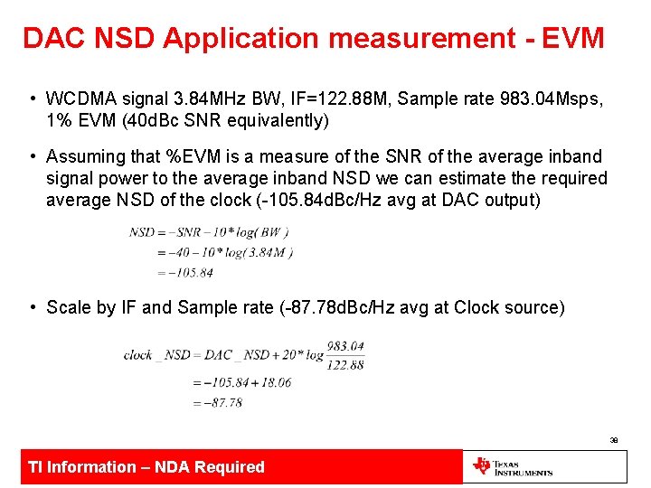
DAC NSD Application measurement - EVM • WCDMA signal 3. 84 MHz BW, IF=122. 88 M, Sample rate 983. 04 Msps, 1% EVM (40 d. Bc SNR equivalently) • Assuming that %EVM is a measure of the SNR of the average inband signal power to the average inband NSD we can estimate the required average NSD of the clock (-105. 84 d. Bc/Hz avg at DAC output) • Scale by IF and Sample rate (-87. 78 d. Bc/Hz avg at Clock source) 38 TI Information – NDA Required

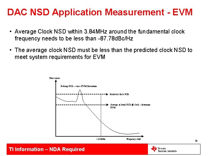
DAC NSD Application Measurement - EVM • Average Clock NSD within 3. 84 MHz around the fundamental clock frequency needs to be less than -87. 78 d. Bc/Hz • The average clock NSD must be less than the predicted clock NSD to meet system requirements for EVM Phase noise Peaking NSD – cause EVM fluctuation Predicted clock NSD Average in-band NSD @ clock – determine EVM 1. 92 MHz TI Information – NDA Required Frequency shift 39

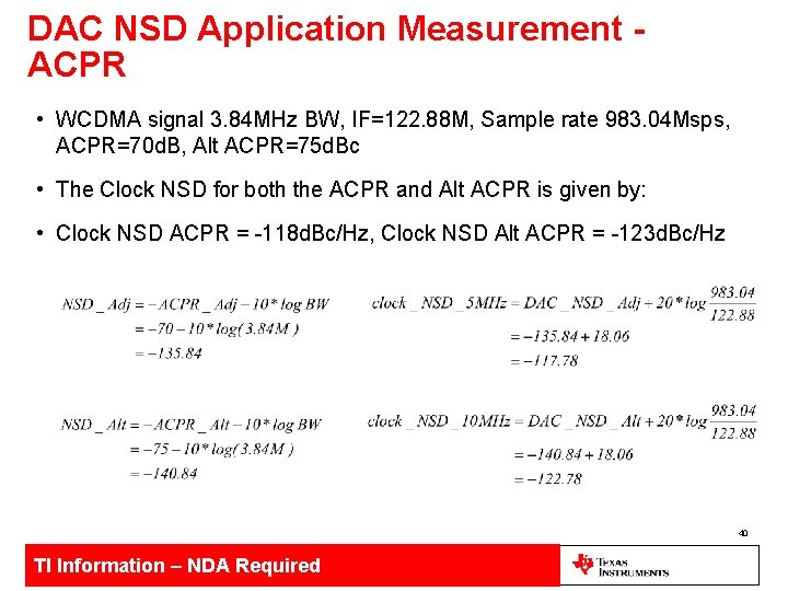
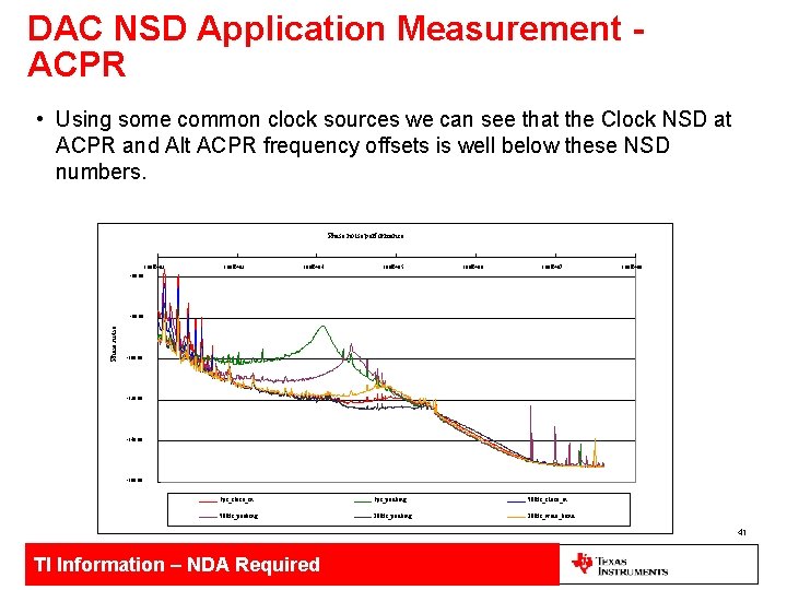
DAC NSD Application Measurement ACPR • WCDMA signal 3. 84 MHz BW, IF=122. 88 M, Sample rate 983. 04 Msps, ACPR=70 d. B, Alt ACPR=75 d. Bc • The Clock NSD for both the ACPR and Alt ACPR is given by: • Clock NSD ACPR = -118 d. Bc/Hz, Clock NSD Alt ACPR = -123 d. Bc/Hz 40 TI Information – NDA Required

DAC NSD Application Measurement ACPR • Using some common clock sources we can see that the Clock NSD at ACPR and Alt ACPR frequency offsets is well below these NSD numbers. Phase noise performance 1. 00 E+02 1. 00 E+03 1. 00 E+04 1. 00 E+05 1. 00 E+06 1. 00 E+07 1. 00 E+08 -60. 00 Phase noise -80. 00 -100. 00 -120. 00 -140. 00 -160. 00 1 ps_close_in 1 ps_peaking 500 fs_close_in 500 fs_peaking 200 fs_wide_band 41 TI Information – NDA Required

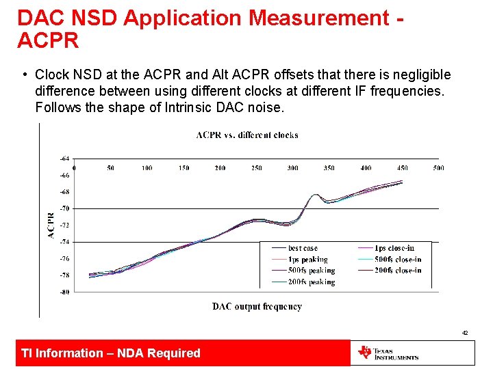
DAC NSD Application Measurement ACPR • Clock NSD at the ACPR and Alt ACPR offsets that there is negligible difference between using different clocks at different IF frequencies. Follows the shape of Intrinsic DAC noise. 42 TI Information – NDA Required

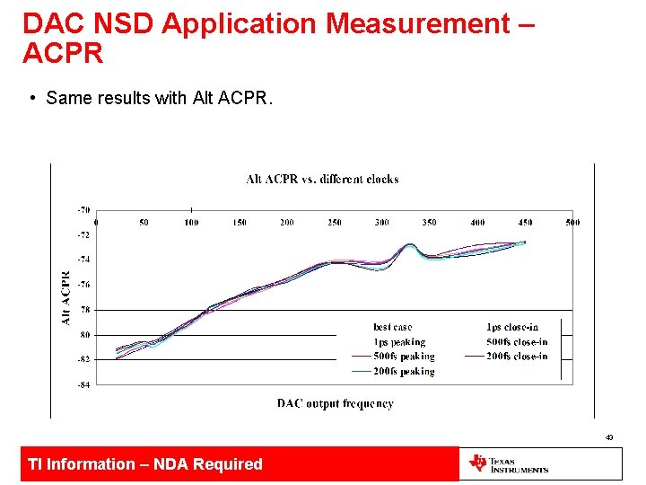
DAC NSD Application Measurement – ACPR • Same results with Alt ACPR. 43 TI Information – NDA Required

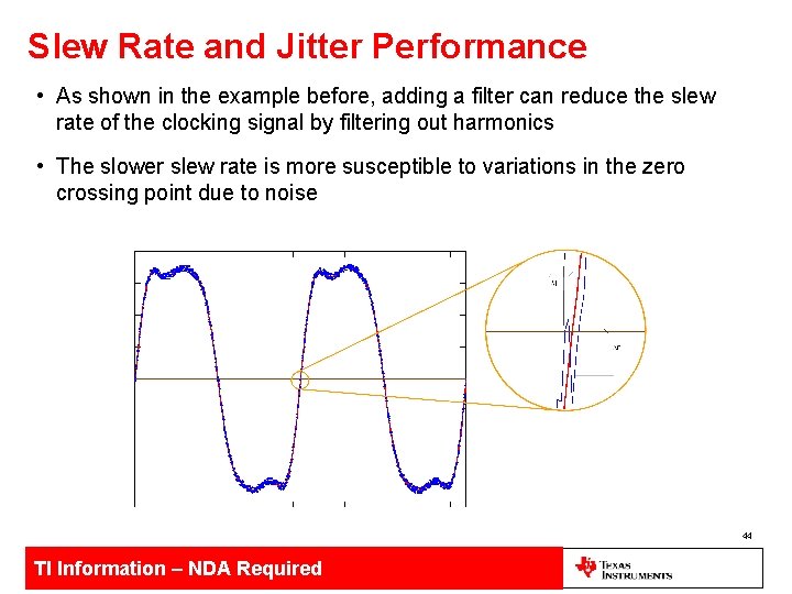
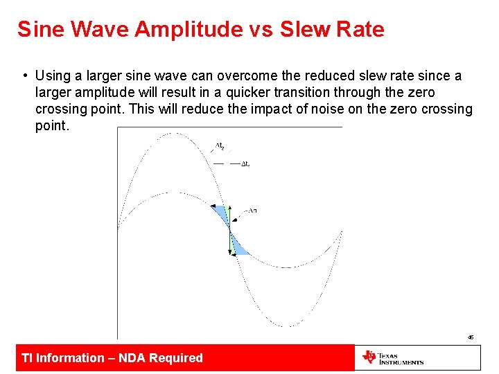
Slew Rate and Jitter Performance • As shown in the example before, adding a filter can reduce the slew rate of the clocking signal by filtering out harmonics • The slower slew rate is more susceptible to variations in the zero crossing point due to noise 44 TI Information – NDA Required

Sine Wave Amplitude vs Slew Rate • Using a larger sine wave can overcome the reduced slew rate since a larger amplitude will result in a quicker transition through the zero crossing point. This will reduce the impact of noise on the zero crossing point. 45 TI Information – NDA Required

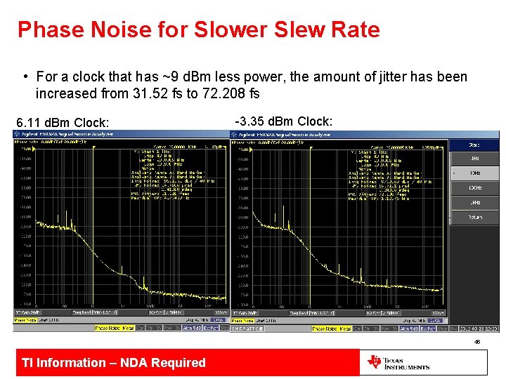
Phase Noise for Slower Slew Rate • For a clock that has ~9 d. Bm less power, the amount of jitter has been increased from 31. 52 fs to 72. 208 fs 6. 11 d. Bm Clock: -3. 35 d. Bm Clock: 46 TI Information – NDA Required

Improving DAC SFDR with Dithering 47 TI Information – NDA Required

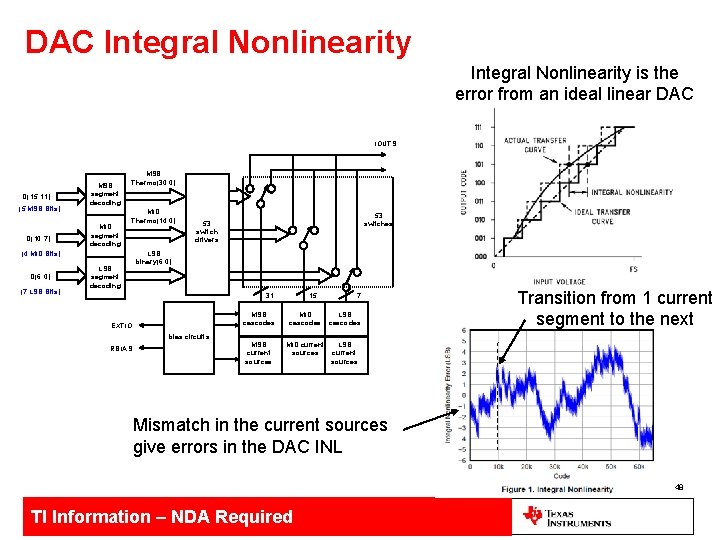
DAC Integral Nonlinearity is the error from an ideal linear DAC IOUTS D(15: 11) (5 MSB Bits) D(10: 7) MSB segment decoding MID segment decoding MSB Thermo(30: 0) MID Thermo(14: 0) (4 MID Bits) D(6: 0) (7 LSB Bits) LSB segment decoding 53 switches 53 switch drivers LSB binary(6: 0) 31 EXTIO bias circuits RBIAS 15 7 MSB cascodes MID cascodes LSB cascodes MSB current sources MID current sources LSB current sources Transition from 1 current segment to the next Mismatch in the current sources give errors in the DAC INL 48 TI Information – NDA Required

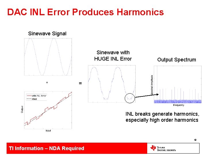
DAC INL Error Produces Harmonics Sinewave Signal Sinewave with HUGE INL Error * Output Spectrum = INL breaks generate harmonics, especially high order harmonics 49 TI Information – NDA Required

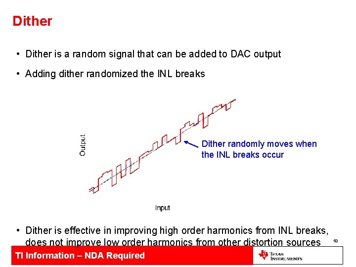
Dither • Dither is a random signal that can be added to DAC output • Adding dither randomized the INL breaks Dither randomly moves when the INL breaks occur • Dither is effective in improving high order harmonics from INL breaks, does not improve low order harmonics from other distortion sources TI Information – NDA Required 50

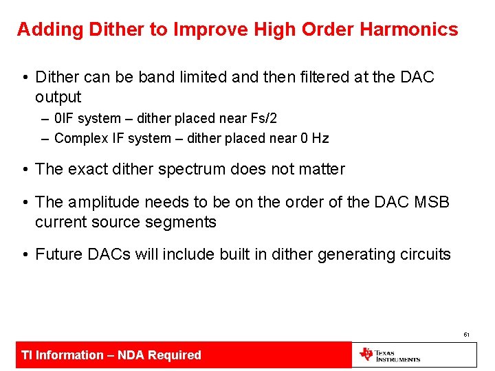
Adding Dither to Improve High Order Harmonics • Dither can be band limited and then filtered at the DAC output – 0 IF system – dither placed near Fs/2 – Complex IF system – dither placed near 0 Hz • The exact dither spectrum does not matter • The amplitude needs to be on the order of the DAC MSB current source segments • Future DACs will include built in dither generating circuits 51 TI Information – NDA Required

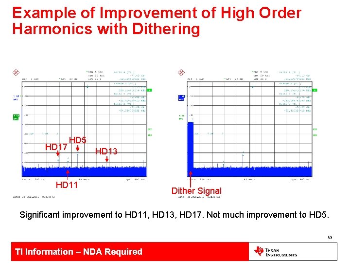
Demonstration of Dither: Setup • TSW 3100+DAC 34 H 84 • Fs=1228. 8 MHz • NCO: disabled • Output signal power: -1. 95 d. Bm • Output signal frequency: 210 MHz • Generation of dithering noise – 200 -tone signal – WCDMA carrier 52 TI Information – NDA Required

Example of Improvement of High Order Harmonics with Dithering HD 17 HD 5 HD 13 HD 11 Dither Signal Significant improvement to HD 11, HD 13, HD 17. Not much improvement to HD 5. 53 TI Information – NDA Required

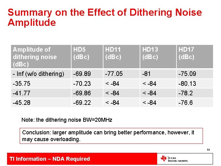
Summary on the Effect of Dithering Noise Amplitude of dithering noise (d. Bc) HD 5 (d. Bc) HD 11 (d. Bc) HD 13 (d. Bc) HD 17 (d. Bc) - Inf (w/o dithering) -69. 89 -77. 05 -81 -75. 09 -35. 75 -70. 23 < -84 -80. 13 -41. 77 -69. 86 < -84 -78. 2 -45. 28 -69. 22 < -84 -76. 6 Note: the dithering noise BW=20 MHz Conclusion: larger amplitude can bring better performance, however, it may cause overloading. 54 TI Information – NDA Required

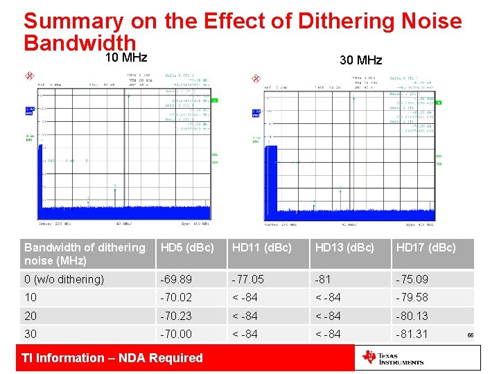
Summary on the Effect of Dithering Noise Bandwidth 10 MHz 30 MHz Bandwidth of dithering noise (MHz) HD 5 (d. Bc) HD 11 (d. Bc) HD 13 (d. Bc) HD 17 (d. Bc) 0 (w/o dithering) -69. 89 -77. 05 -81 -75. 09 10 -70. 02 < -84 -79. 58 20 -70. 23 < -84 -80. 13 30 -70. 00 < -84 -81. 31 TI Information – NDA Required 55

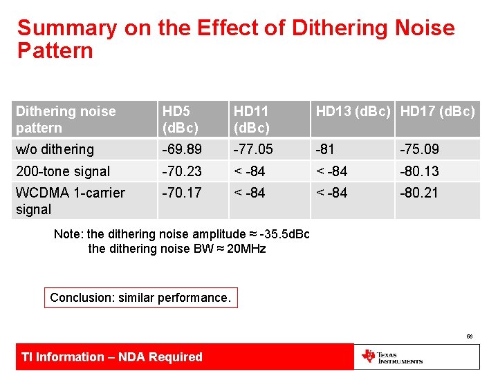
Summary on the Effect of Dithering Noise Pattern Dithering noise pattern HD 5 (d. Bc) HD 11 (d. Bc) HD 13 (d. Bc) HD 17 (d. Bc) w/o dithering -69. 89 -77. 05 -81 -75. 09 200 -tone signal -70. 23 < -84 -80. 13 WCDMA 1 -carrier signal -70. 17 < -84 -80. 21 Note: the dithering noise amplitude ≈ -35. 5 d. Bc the dithering noise BW ≈ 20 MHz Conclusion: similar performance. 56 TI Information – NDA Required

Thank you! 57 TI Information – NDA Required