
A General Purpose Charge Readout Chip for TPC

- Slides: 18
A General Purpose Charge Readout Chip for TPC Applications Luciano Musa, CERN, 10 th September 2007 Outline • Introduction • Circuit overview and architecture • Charge amplifier prototype in 0. 13 mm CMOS • New programmable charge amplifier for LPTPC 10 th September 2007 Luciano Musa 1
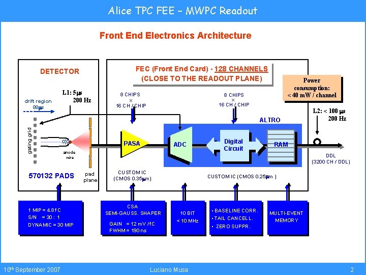
Alice TPC FEE – MWPC Readout Front End Electronics Architecture FEC (Front End Card) - 128 CHANNELS (CLOSE TO THE READOUT PLANE) DETECTOR drift region 88 ms L 1: 5 ms 200 Hz 8 CHIPS x 16 CH / CHIP Power consumption: < 40 m. W / channel 8 CHIPS x 16 CH / CHIP gating grid ALTRO PASA anode wire 570132 PADS 1 MIP = 4. 8 f. C S/N = 30 : 1 DYNAMIC = 30 MIP 10 th September 2007 ADC Digital Circuit L 2: < 100 ms 200 Hz RAM DDL (3200 CH / DDL) pad plane CUSTOM IC (CMOS 0. 35 mm) CSA SEMI-GAUSS. SHAPER GAIN = 12 m. V / f. C FWHM = 190 ns CUSTOM IC (CMOS 0. 25 mm ) 10 BIT < 10 MHz Luciano Musa • BASELINE CORR. • TAIL CANCELL. • ZERO SUPPR. MULTI-EVENT MEMORY 2
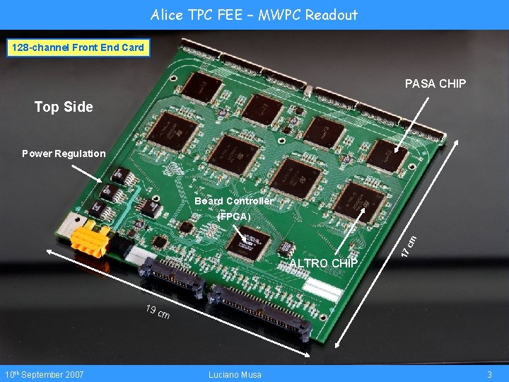
Alice TPC FEE – MWPC Readout 128 -channel Front End Card PASA CHIP Top Side Power Regulation Board Controller ALTRO CHIP 19 10 th September 2007 17 cm (FPGA) cm Luciano Musa 3
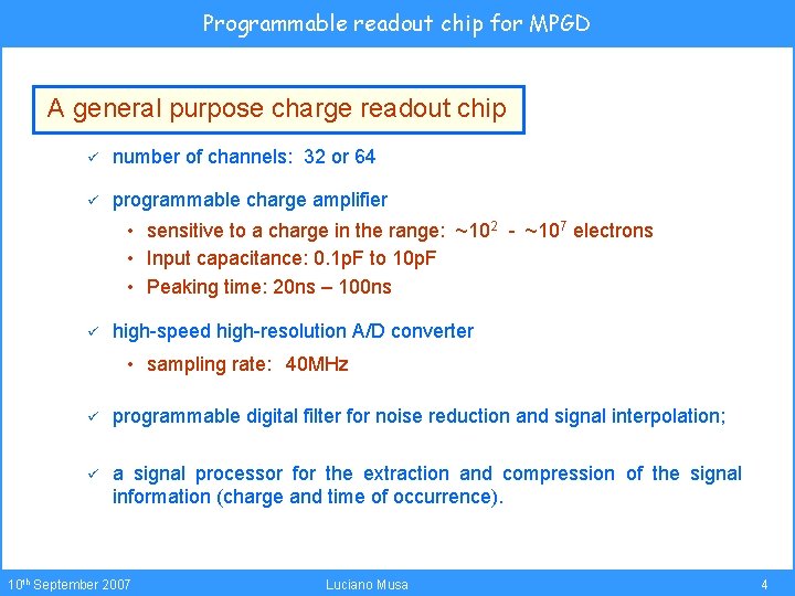
Programmable readout chip for MPGD A general purpose charge readout chip ü number of channels: 32 or 64 ü programmable charge amplifier • sensitive to a charge in the range: ~102 - ~107 electrons • Input capacitance: 0. 1 p. F to 10 p. F • Peaking time: 20 ns – 100 ns ü high-speed high-resolution A/D converter • sampling rate: 40 MHz ü programmable digital filter for noise reduction and signal interpolation; ü a signal processor for the extraction and compression of the signal information (charge and time of occurrence). 10 th September 2007 Luciano Musa 4
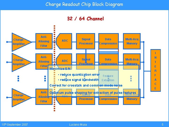
Charge Readout Chip Block Diagram 32 / 64 Channel Charge Amplifier Anti. Aliasing ADC Filter Signal Data Multi-Acq Processor Compression Memory I Charge Amplifier Anti. Aliasing Filter Signal ADC Processor Hit. Data Finder Compression Multi-Acq Memory Maximize S/N • reduce quantization error Feature • reduce signal bandwidth Extaction Correct for crosstalk and common mode noise Charge Amplifier 10 th September 2007 N T E R F A C E Anti- Optimum pulse shaping for extraction of pulse features Signal Data Multi-Acq Histogrammer ADC Aliasing Processor Compression Memory Filter Luciano Musa 5
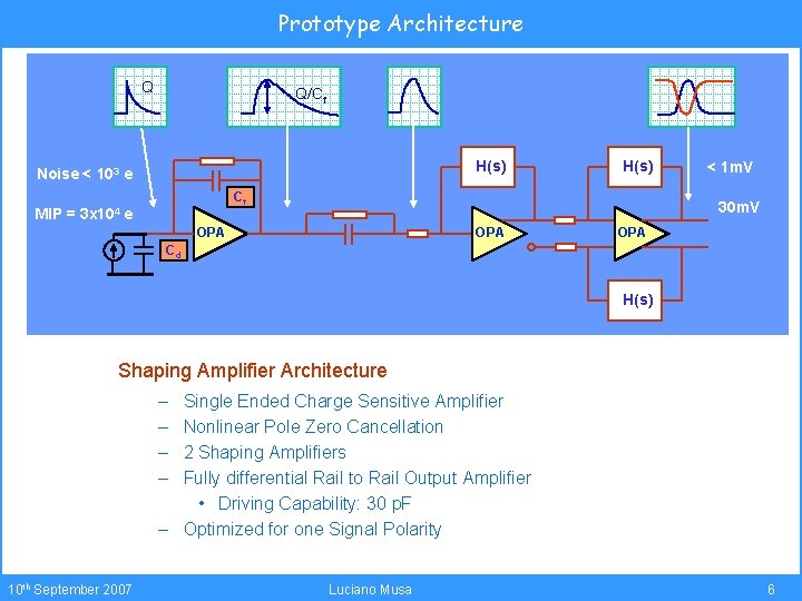
Prototype Architecture Q Q/Cf H(s) Noise < 103 e MIP = H(s) Cf 3 x 10⁴ e < 1 m. V 30 m. V OPA OPA Cd H(s) Shaping Amplifier Architecture – – Single Ended Charge Sensitive Amplifier Nonlinear Pole Zero Cancellation 2 Shaping Amplifiers Fully differential Rail to Rail Output Amplifier • Driving Capability: 30 p. F – Optimized for one Signal Polarity 10 th September 2007 Luciano Musa 6
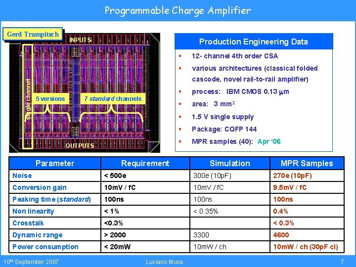
Programmable Charge Amplifier single channel Gerd Trampitsch INPUTS Production Engineering Data § 12 - channel 4 th order CSA § various architectures (classical folded cascode, novel rail-to-rail amplifier) 5 versions 7 standard channels OUTPUTS Parameter § process: IBM CMOS 0. 13 mm § area: 3 mm 2 § 1. 5 V single supply § Package: CQFP 144 § MPR samples (40): Apr ‘ 06 Requirement Simulation MPR Samples Noise < 500 e 300 e (10 p. F) 270 e (10 p. F) Conversion gain 10 m. V / f. C 9. 5 m. V / f. C Peaking time (standard) 100 ns Non linearity < 1% < 0. 35% 0. 4% Crosstalk <0. 3% Dynamic range > 2000 3300 4600 Power consumption < 20 m. W 10 m. W / ch (30 p. F cl) 10 th September 2007 < 0. 3% Luciano Musa 7
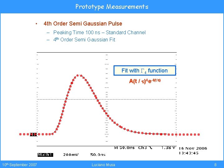
Prototype Measurements • 4 th Order Semi Gaussian Pulse – Peaking Time 100 ns – Standard Channel – 4 th Order Semi Gaussian Fit with G 4 function A(t / t)4 e-4(t/t) 10 th September 2007 Luciano Musa 8
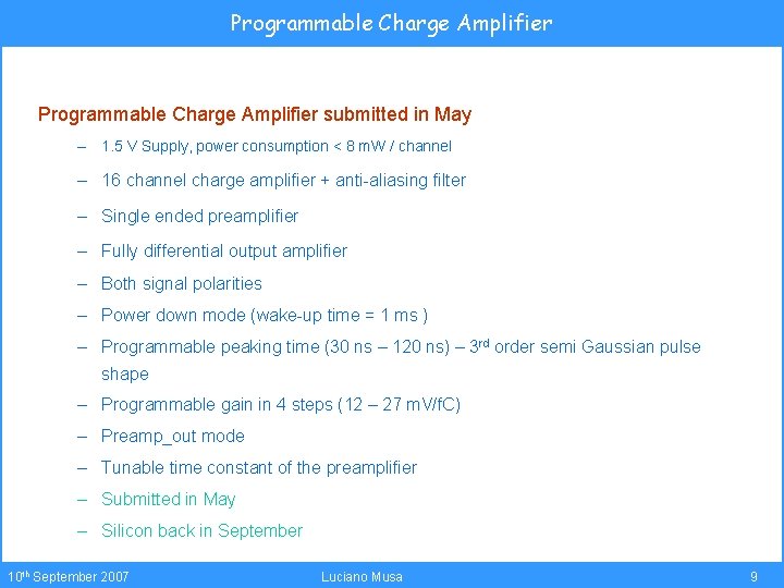
Programmable Charge Amplifier submitted in May – 1. 5 V Supply, power consumption < 8 m. W / channel – 16 channel charge amplifier + anti-aliasing filter – Single ended preamplifier – Fully differential output amplifier – Both signal polarities – Power down mode (wake-up time = 1 ms ) – Programmable peaking time (30 ns – 120 ns) – 3 rd order semi Gaussian pulse shape – Programmable gain in 4 steps (12 – 27 m. V/f. C) – Preamp_out mode – Tunable time constant of the preamplifier – Submitted in May – Silicon back in September 10 th September 2007 Luciano Musa 9
Programmable Charge Amplifier • Programmable Peaking Time – 30 to 120 ns 10 th September 2007 Luciano Musa 10
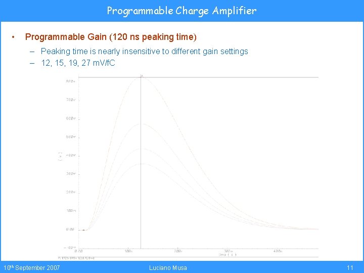
Programmable Charge Amplifier • Programmable Gain (120 ns peaking time) – Peaking time is nearly insensitive to different gain settings – 12, 15, 19, 27 m. V/f. C 10 th September 2007 Luciano Musa 11
Programmable Charge Amplifier • Programmable Gain (30 ns peaking time) – Peaking time is nearly insensitive to different gain settings – 11, 14, 18, 25 m. V/f. C 10 th September 2007 Luciano Musa 12
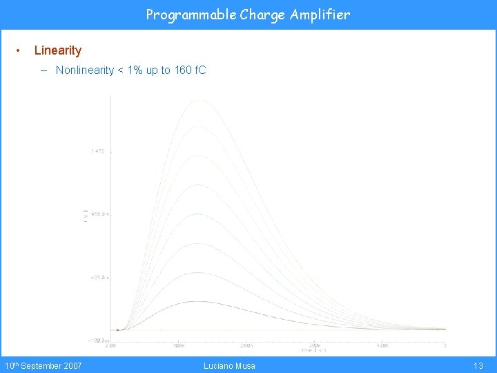
Programmable Charge Amplifier • Linearity – Nonlinearity < 1% up to 160 f. C 10 th September 2007 Luciano Musa 13
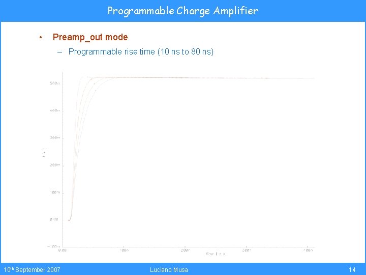
Programmable Charge Amplifier • Preamp_out mode – Programmable rise time (10 ns to 80 ns) 10 th September 2007 Luciano Musa 14
Programmable Charge Amplifier • Preamp_out mode – Programmable gain (5. 3 m. V/f. C to 6. 8 m. V/f. C) 10 th September 2007 Luciano Musa 15
Programmable Charge Amplifier • Preamp Decay Time – Preamp_out mode – Continuously programmable 10 th September 2007 Luciano Musa 16
Programmable Charge Amplifier 10 th September 2007 Luciano Musa 17
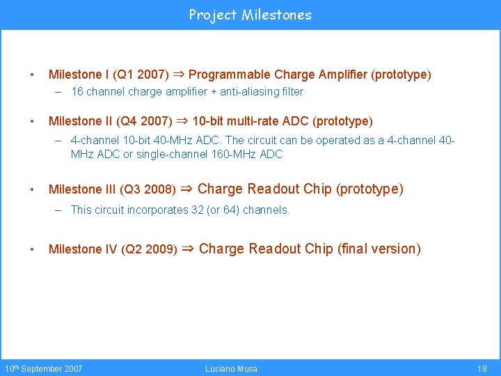
Project Milestones • Milestone I (Q 1 2007) ⇒ Programmable Charge Amplifier (prototype) – 16 channel charge amplifier + anti-aliasing filter • Milestone II (Q 4 2007) ⇒ 10 -bit multi-rate ADC (prototype) – 4 -channel 10 -bit 40 -MHz ADC. The circuit can be operated as a 4 -channel 40 MHz ADC or single-channel 160 -MHz ADC • Milestone III (Q 3 2008) ⇒ Charge Readout Chip (prototype) – This circuit incorporates 32 (or 64) channels. • Milestone IV (Q 2 2009) ⇒ Charge Readout Chip (final version) 10 th September 2007 Luciano Musa 18