Schematic and Layout Tips Agenda Schematic Tips ADC




- Slides: 78

Schematic and Layout Tips

Agenda Schematic Tips • • • ADC Schematics DAC Schematics RF Schematics PCB Layout Recommendations • General Guidelines • • Trace Routing Part Placement Layer Stack-up Cooling Trouble Shooting Help

ADC Schematics Analog Input Power Supply Clocking

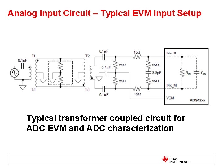
Analog Input Circuit – Typical EVM Input Setup Typical transformer coupled circuit for ADC EVM and ADC characterization

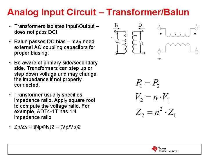
Analog Input Circuit – Transformer/Balun • Transformers isolates InputOutput – does not pass DC! • Balun passes DC bias – may need external AC coupling capacitors for proper biasing. • Be aware of primary side/secondary side. Transformers can step up or step down voltage and may change the impedance if not properly connected. • Transformer usually specifies impedance ratio. Apply square root to compute the voltage ratio. For example, ADT 4 -1 T has 1: 4 impedance ratio • Zp/Zs = (Np/Ns)2 = (Vp/Vs)2

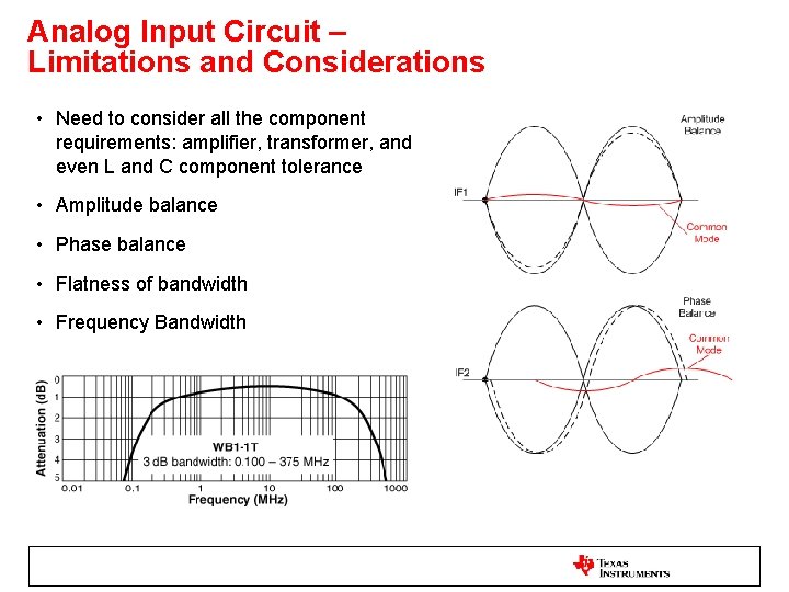
Analog Input Circuit – Limitations and Considerations • Need to consider all the component requirements: amplifier, transformer, and even L and C component tolerance • Amplitude balance • Phase balance • Flatness of bandwidth • Frequency Bandwidth

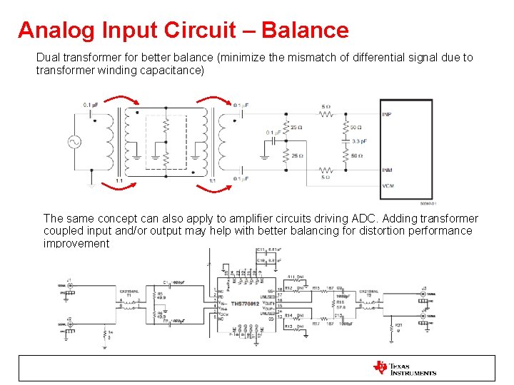
Analog Input Circuit – Balance Dual transformer for better balance (minimize the mismatch of differential signal due to transformer winding capacitance) The same concept can also apply to amplifier circuits driving ADC. Adding transformer coupled input and/or output may help with better balancing for distortion performance improvement

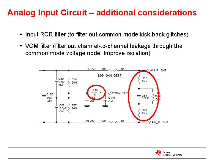
Analog Input Circuit – additional considerations • Input RCR filter (to filter out common mode kick-back glitches) • VCM filter (filter out channel-to-channel leakage through the common mode voltage node. Improve isolation)

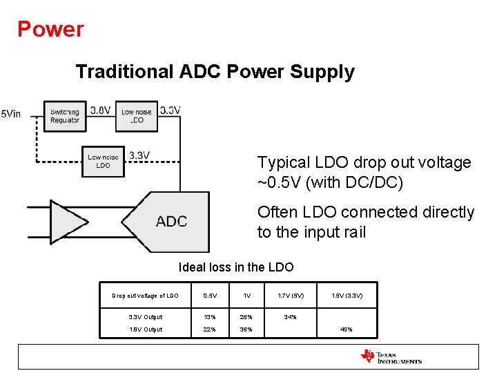
Power Traditional ADC Power Supply Typical LDO drop out voltage ~0. 5 V (with DC/DC) Often LDO connected directly to the input rail Ideal loss in the LDO Drop out voltage of LDO 0. 5 V 1 V 1. 7 V (5 V) 3. 3 V Output 13% 26% 34% 1. 8 V Output 22% 36% 1. 5 V (3. 3 V) 45%

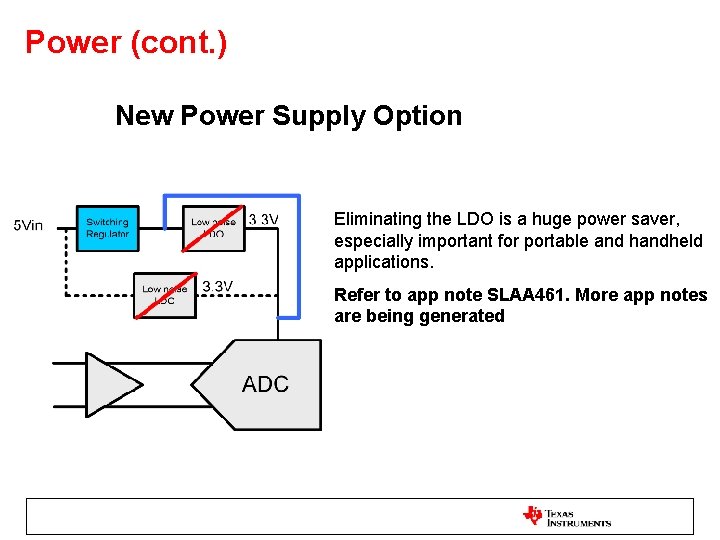
Power (cont. ) New Power Supply Option Eliminating the LDO is a huge power saver, especially important for portable and handheld applications. Refer to app note SLAA 461. More app notes are being generated

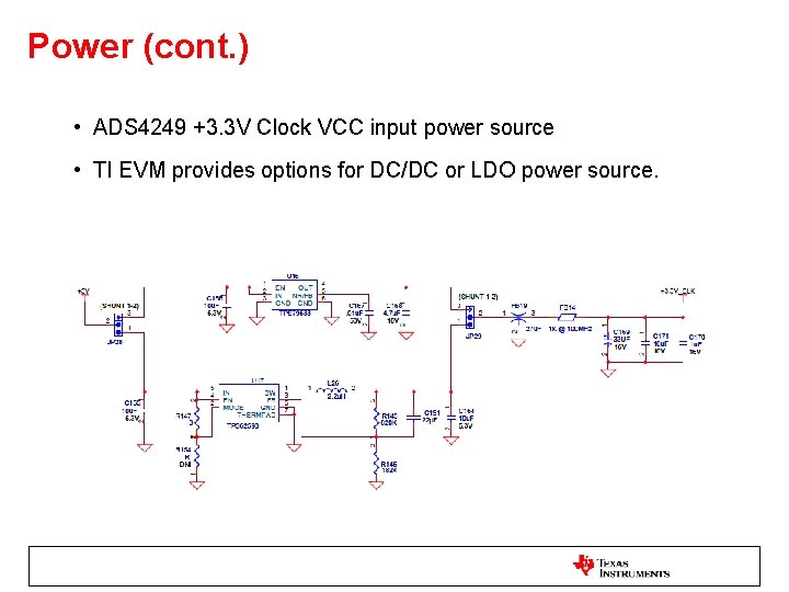
Power (cont. ) • ADS 4249 +3. 3 V Clock VCC input power source • TI EVM provides options for DC/DC or LDO power source.

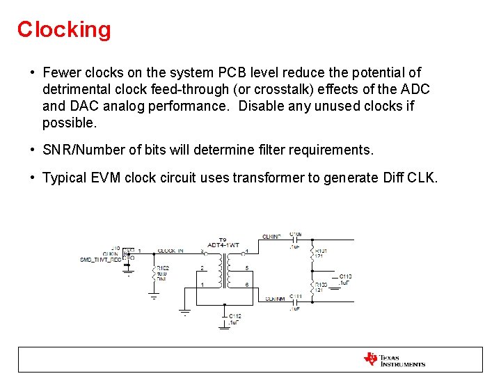
Clocking • Fewer clocks on the system PCB level reduce the potential of detrimental clock feed-through (or crosstalk) effects of the ADC and DAC analog performance. Disable any unused clocks if possible. • SNR/Number of bits will determine filter requirements. • Typical EVM clock circuit uses transformer to generate Diff CLK.

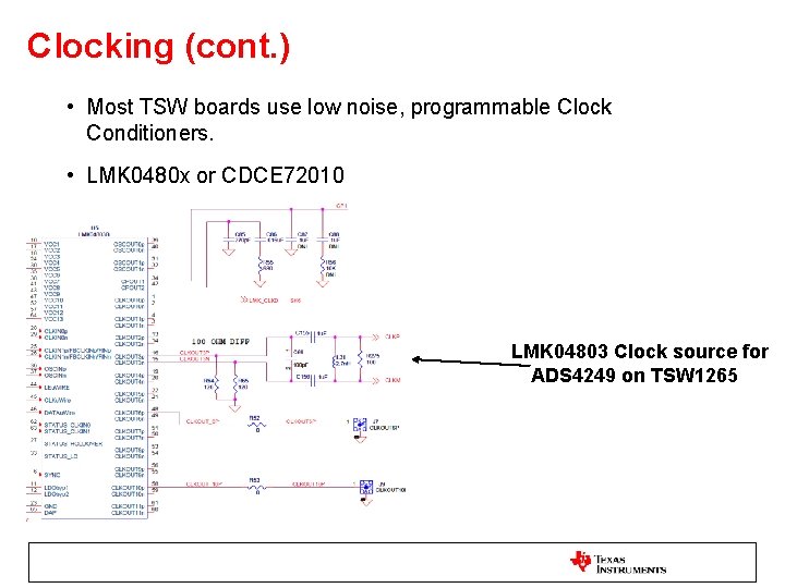
Clocking (cont. ) • Most TSW boards use low noise, programmable Clock Conditioners. • LMK 0480 x or CDCE 72010 LMK 04803 Clock source for ADS 4249 on TSW 1265

DAC Schematics Digital Input Analog Output Clocking

Digital Input • All signals should be matched to have the same trace length. • The matching of trace length between the LVDS pairs are typically no more than +/- 10 mils. • The overall length of the trace is not critical. Maintaining the same length for all signals is more important. • Most newer EVM’s provide options to delay the DATACLK (changing trace length) to help meet setup and hold requirements. • Add probe points on CLK and data lines if possible for trouble shooting.

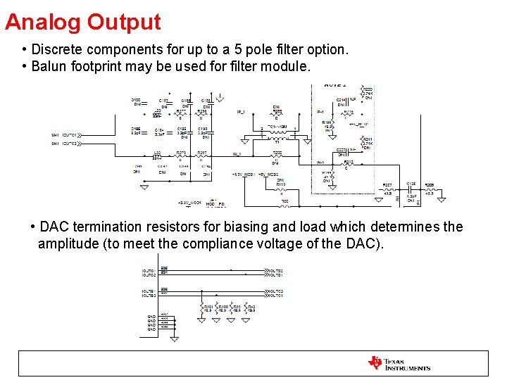
Analog Output • Discrete components for up to a 5 pole filter option. • Balun footprint may be used for filter module. • DAC termination resistors for biasing and load which determines the amplitude (to meet the compliance voltage of the DAC).

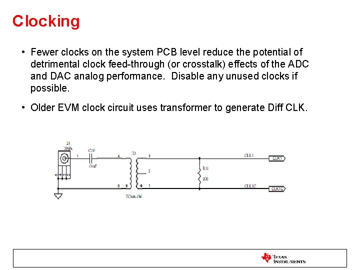
Clocking • Fewer clocks on the system PCB level reduce the potential of detrimental clock feed-through (or crosstalk) effects of the ADC and DAC analog performance. Disable any unused clocks if possible. • Older EVM clock circuit uses transformer to generate Diff CLK.

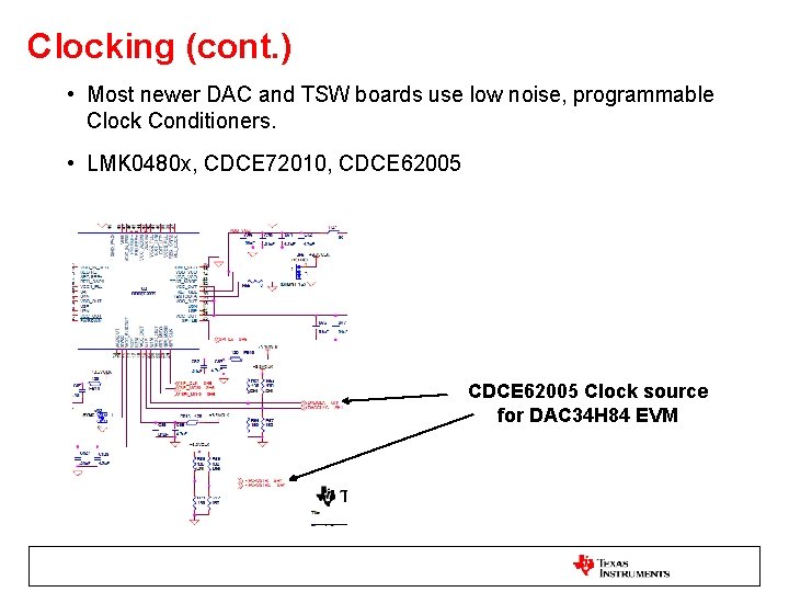
Clocking (cont. ) • Most newer DAC and TSW boards use low noise, programmable Clock Conditioners. • LMK 0480 x, CDCE 72010, CDCE 62005 Clock source for DAC 34 H 84 EVM

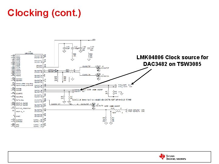
Clocking (cont. ) LMK 04806 Clock source for DAC 3482 on TSW 3085

RF Schematics DAC 348 x to Modulator Interface RF Output Power Supply LO Source

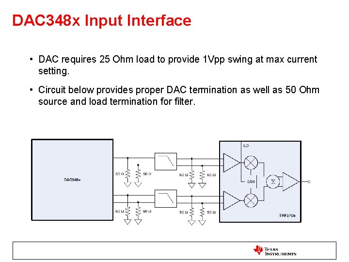
DAC 348 x Input Interface • DAC requires 25 Ohm load to provide 1 Vpp swing at max current setting. • Circuit below provides proper DAC termination as well as 50 Ohm source and load termination for filter.

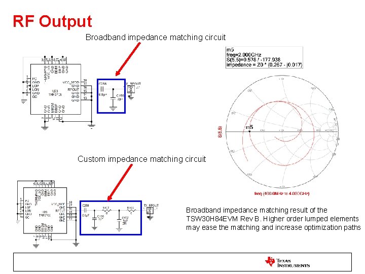
RF Output Broadband impedance matching circuit Custom impedance matching circuit Broadband impedance matching result of the TSW 30 H 84 EVM Rev B. Higher order lumped elements may ease the matching and increase optimization paths

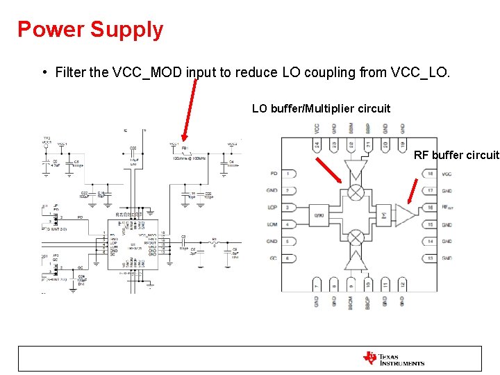
Power Supply • Filter the VCC_MOD input to reduce LO coupling from VCC_LO. LO buffer/Multiplier circuit RF buffer circuit

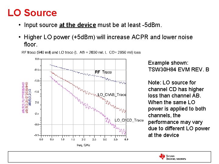
LO Source • Input source at the device must be at least -5 d. Bm. • Higher LO power (+5 d. Bm) will increase ACPR and lower noise floor. Example shown: TSW 30 H 84 EVM REV. B Note: LO source for channel CD has higher loss than channel AB. When the same LO power is applied to both channels, the performance may vary due to different LO power at the device

PCB Layout Recommendations General Guidelines Trace Routing Part Placement Layer Stackup Cooling

General Guidelines • Try to keep High power/frequency signals (> 0 d. Bm) away from any low power/frequency signals (< 0 d. Bm) as much as possible. • Share pads if possible to remove stub length. • Analog in one area, Digital in another. • Place parts that are connected together close as possible (result in shorter traces, less chance for reflections). • IC’s routing to connectors should be placed near their respective connector. • Route high speed differential lines on internal layers for better noise suppression. These signals must have unbroken reference impedance planes above and below them to maintain the proper impedance.

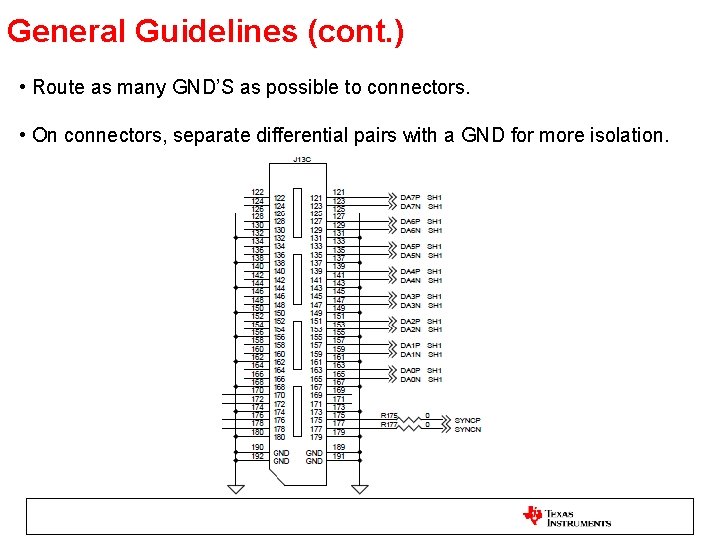
General Guidelines (cont. ) • Route as many GND’S as possible to connectors. • On connectors, separate differential pairs with a GND for more isolation.

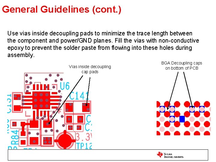
General Guidelines (cont. ) Use vias inside decoupling pads to minimize the trace length between the component and power/GND planes. Fill the vias with non-conductive epoxy to prevent the solder paste from flowing into these holes during assembly. Vias inside decoupling cap pads BGA Decoupling caps on bottom of PCB

General Guidelines (cont. ) Add multiple large (10 -12 mil) vias in power pads. 8 mil via w/ standard plating will carry approximately 1 amp. 18 mil via a little more than 2 amps. Use multiple vias on large surface mount pads needs multiple vias if they are connected to internal power or ground layers. Shape to shape constraints need to have a default clearance of 20 mils. Impedance traces may reference to a split plane (shape) but must never cross over the split. Differential pair to differential pair spacing should be twice the spacing of the individual pair. Example: 100 ohm differential trace is 4. 6 mil with 7. 40 mil spacing. Pair to pair spacing should be 14. 8 mils or greater. Avoid long parallel nets > 500 mils. Avoid broadside coupling on adjacent stripline layers. Route one of the layers orthogonally to minimize coupled regions. Route noisy signals on stripline (internal plane) rather than microstrip (top/bottom layer) to reduce EMI. Ideally have ground planes above and below a power plane. Check ground pours for fingers of ground plane that do not have a ground via at the end of the finger. These can be transmission lines so add a via or delete the finger.

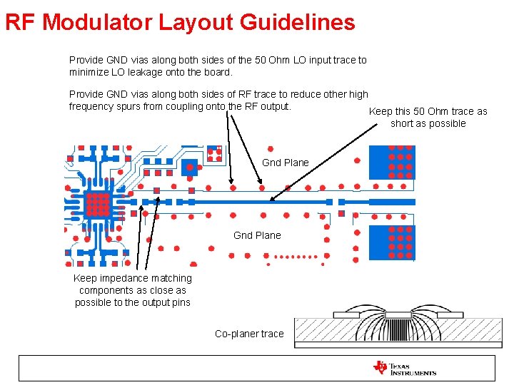
RF Modulator Layout Guidelines Provide GND vias along both sides of the 50 Ohm LO input trace to minimize LO leakage onto the board. Provide GND vias along both sides of RF trace to reduce other high frequency spurs from coupling onto the RF output. Keep this 50 Ohm trace as short as possible Gnd Plane Keep impedance matching components as close as possible to the output pins Co-planer trace

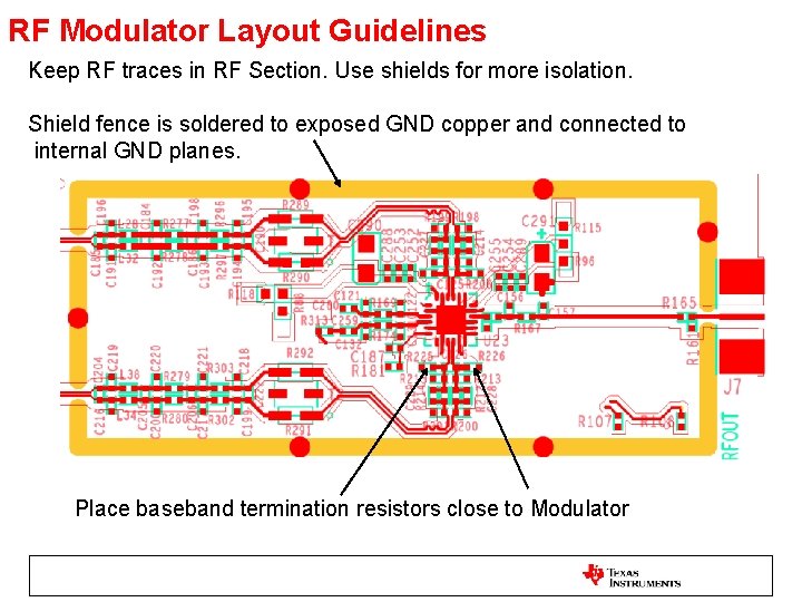
RF Modulator Layout Guidelines Keep RF traces in RF Section. Use shields for more isolation. Shield fence is soldered to exposed GND copper and connected to internal GND planes. Place baseband termination resistors close to Modulator

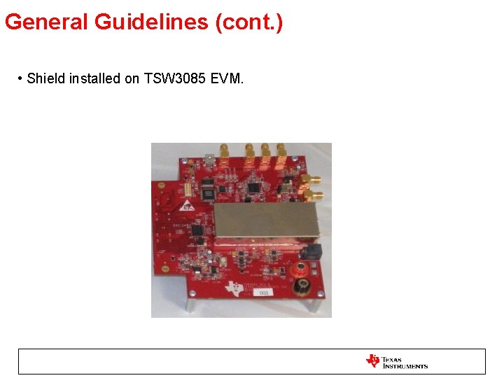
General Guidelines (cont. ) • Shield installed on TSW 3085 EVM.

Trace Routing • Minimize parasitic and maintain impedance by routing the trace with no vias if possible. • Route traces as short as possible. • Use a single solid GND plane (no breaks) under the top and bottom layer signals to keep the impedance constant. Inner layer differential traces must have solid GND planes above and below the signal.

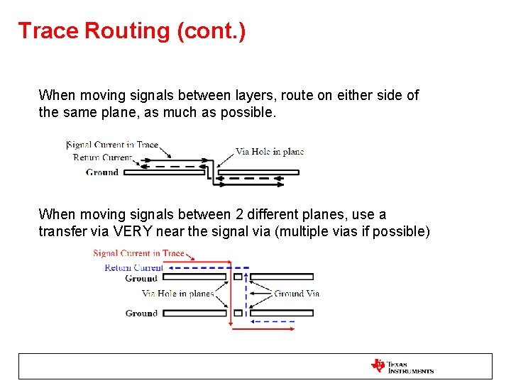
Trace Routing (cont. ) When moving signals between layers, route on either side of the same plane, as much as possible. When moving signals between 2 different planes, use a transfer via VERY near the signal via (multiple vias if possible)

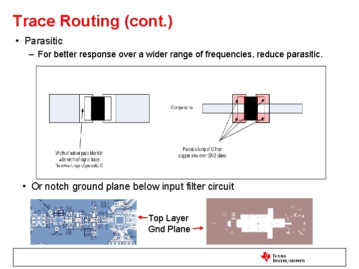
Trace Routing (cont. ) • Parasitic – For better response over a wider range of frequencies, reduce parasitic. • Or notch ground plane below input filter circuit Top Layer Gnd Plane

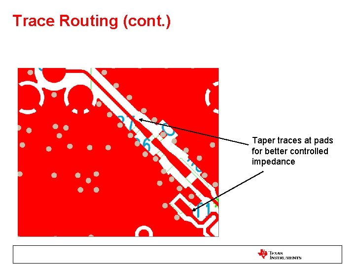
Trace Routing (cont. ) Taper traces at pads for better controlled impedance

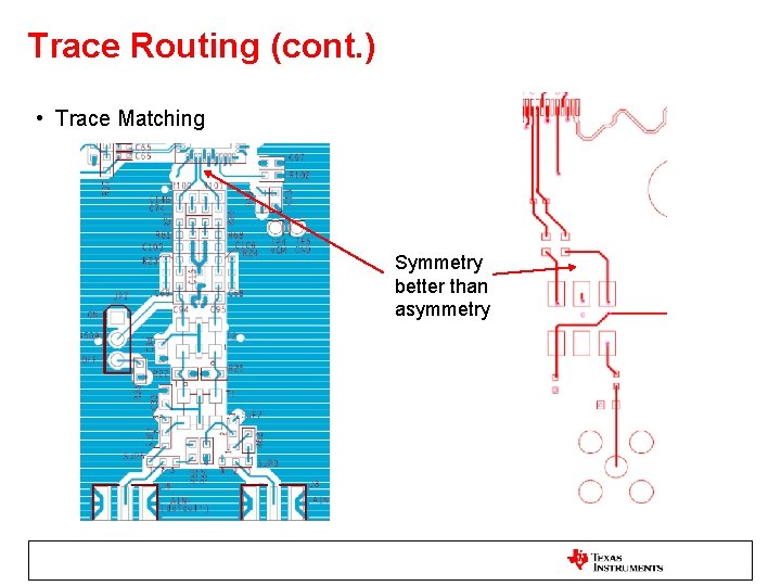
Trace Routing (cont. ) • Trace Matching Symmetry better than asymmetry

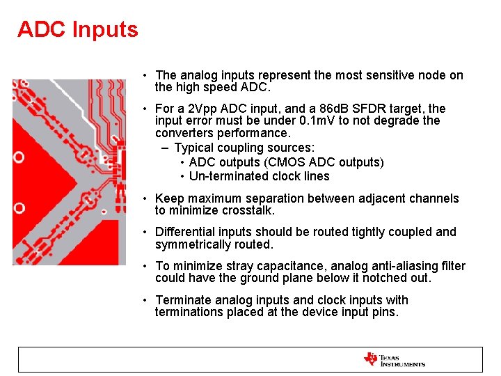
ADC Inputs • The analog inputs represent the most sensitive node on the high speed ADC. • For a 2 Vpp ADC input, and a 86 d. B SFDR target, the input error must be under 0. 1 m. V to not degrade the converters performance. – Typical coupling sources: • ADC outputs (CMOS ADC outputs) • Un-terminated clock lines • Keep maximum separation between adjacent channels to minimize crosstalk. • Differential inputs should be routed tightly coupled and symmetrically routed. • To minimize stray capacitance, analog anti-aliasing filter could have the ground plane below it notched out. • Terminate analog inputs and clock inputs with terminations placed at the device input pins.

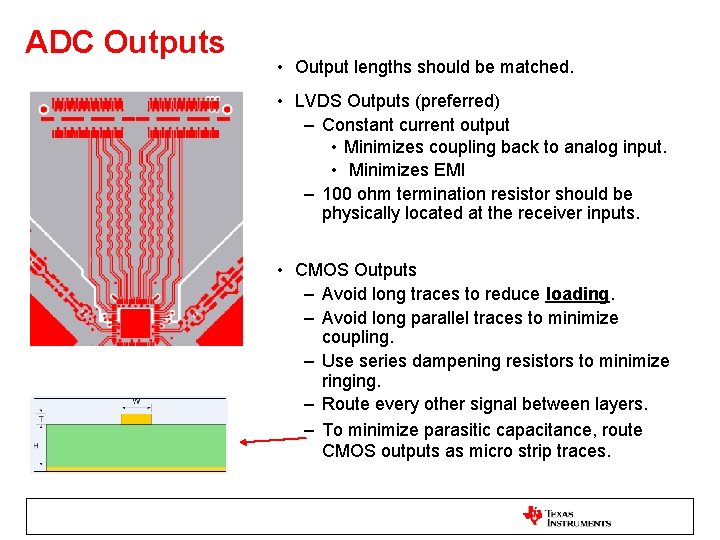
ADC Outputs • Output lengths should be matched. • LVDS Outputs (preferred) – Constant current output • Minimizes coupling back to analog input. • Minimizes EMI – 100 ohm termination resistor should be physically located at the receiver inputs. • CMOS Outputs – Avoid long traces to reduce loading. – Avoid long parallel traces to minimize coupling. – Use series dampening resistors to minimize ringing. – Route every other signal between layers. – To minimize parasitic capacitance, route CMOS outputs as micro strip traces.

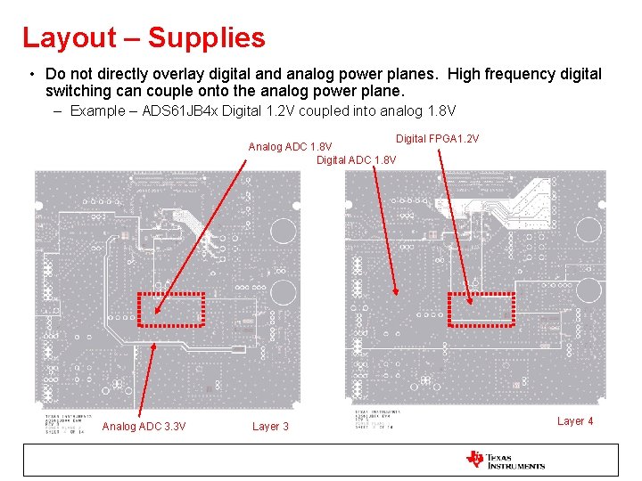
Layout – Supplies • Do not directly overlay digital and analog power planes. High frequency digital switching can couple onto the analog power plane. – Example – ADS 61 JB 4 x Digital 1. 2 V coupled into analog 1. 8 V Digital FPGA 1. 2 V Analog ADC 1. 8 V Digital ADC 1. 8 V Analog ADC 3. 3 V Layer 3 Layer 4

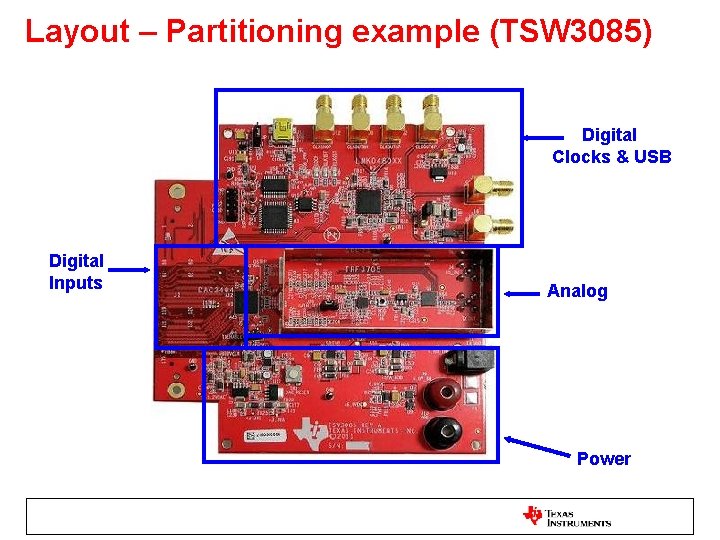
Layout – Partitioning example (TSW 3085) Digital Clocks & USB Digital Inputs Analog Power

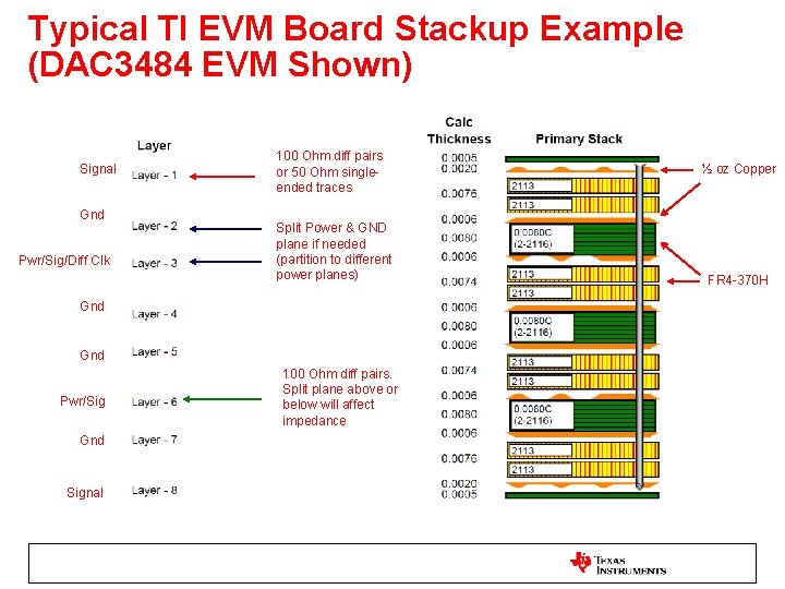
Typical TI EVM Board Stackup Example (DAC 3484 EVM Shown) Signal Gnd Pwr/Sig/Diff Clk 100 Ohm diff pairs or 50 Ohm singleended traces Split Power & GND plane if needed (partition to different power planes) Gnd Pwr/Sig Gnd Signal 100 Ohm diff pairs. Split plane above or below will affect impedance ½ oz Copper FR 4 -370 H

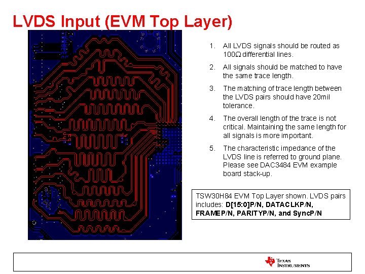
LVDS Input (EVM Top Layer) 1. All LVDS signals should be routed as 100 W differential lines. 2. All signals should be matched to have the same trace length. 3. The matching of trace length between the LVDS pairs should have 20 mil tolerance. 4. The overall length of the trace is not critical. Maintaining the same length for all signals is more important. 5. The characteristic impedance of the LVDS line is referred to ground plane. Please see DAC 3484 EVM example board stack-up. TSW 30 H 84 EVM Top Layer shown. LVDS pairs includes: D[15: 0]P/N, DATACLKP/N, FRAMEP/N, PARITYP/N, and Sync. P/N

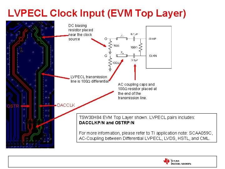
LVPECL Clock Input (EVM Top Layer) DC biasing resistor placed near the clock source LVPECL transmission line is 100 W differential OSTR AC coupling caps and 100 W resistor placed at the end of the transmission line. DACCLK TSW 30 H 84 EVM Top Layer shown. LVPECL pairs includes: DACCLKP/N and OSTRP/N For more information, please refer to TI application note: SCAA 059 C, AC-Coupling between Differential LVPECL, LVDS, HSTL, and CML.

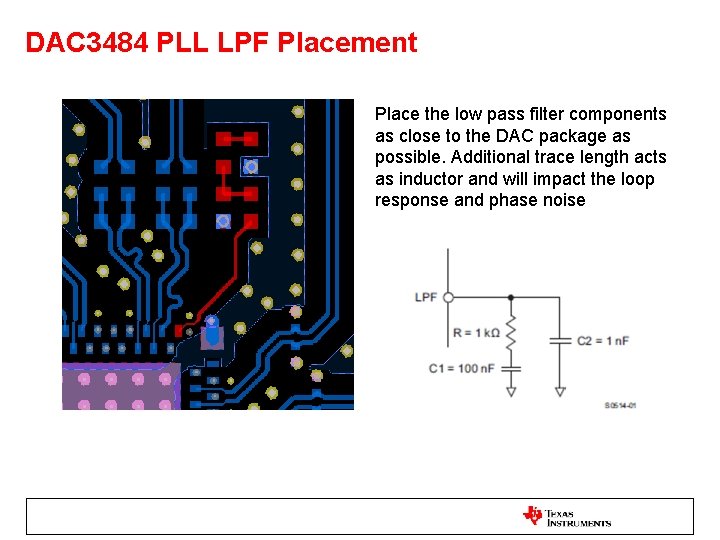
DAC 3484 PLL LPF Placement Place the low pass filter components as close to the DAC package as possible. Additional trace length acts as inductor and will impact the loop response and phase noise

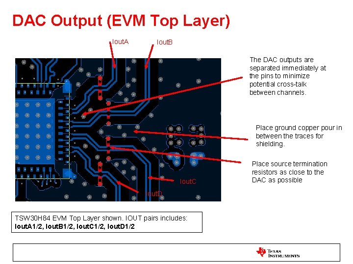
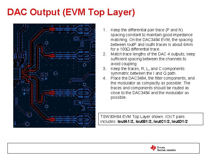
DAC Output (EVM Top Layer) Iout. A Iout. B The DAC outputs are separated immediately at the pins to minimize potential cross-talk between channels. Place ground copper pour in between the traces for shielding. Iout. C Iout. D TSW 30 H 84 EVM Top Layer shown. IOUT pairs includes: Iout. A 1/2, Iout. B 1/2, Iout. C 1/2, Iout. D 1/2 Place source termination resistors as close to the DAC as possible

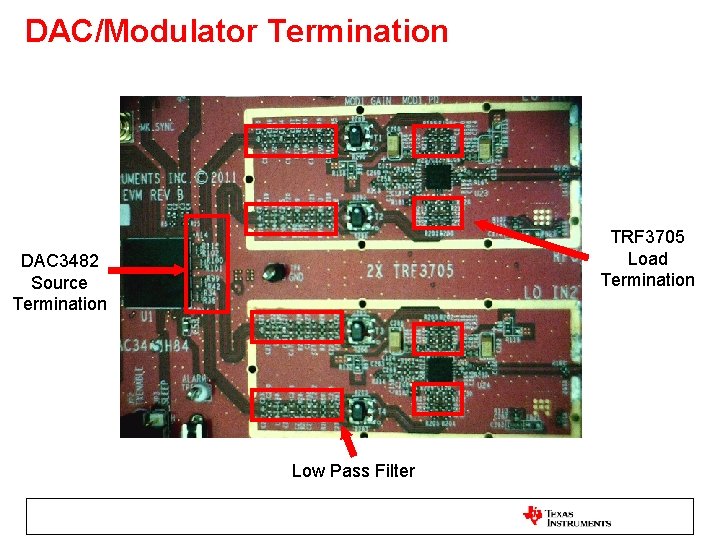
DAC/Modulator Termination TRF 3705 Load Termination DAC 3482 Source Termination Low Pass Filter

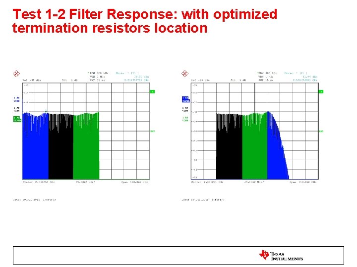
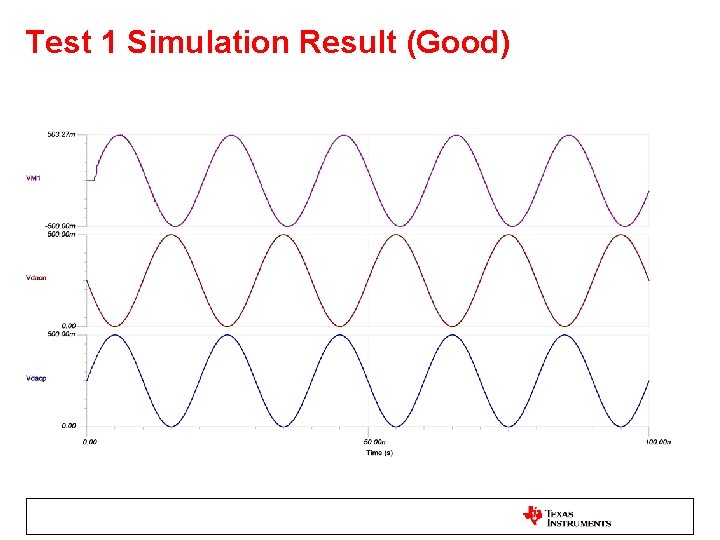
Test 1 -2 Filter Response: with optimized termination resistors location

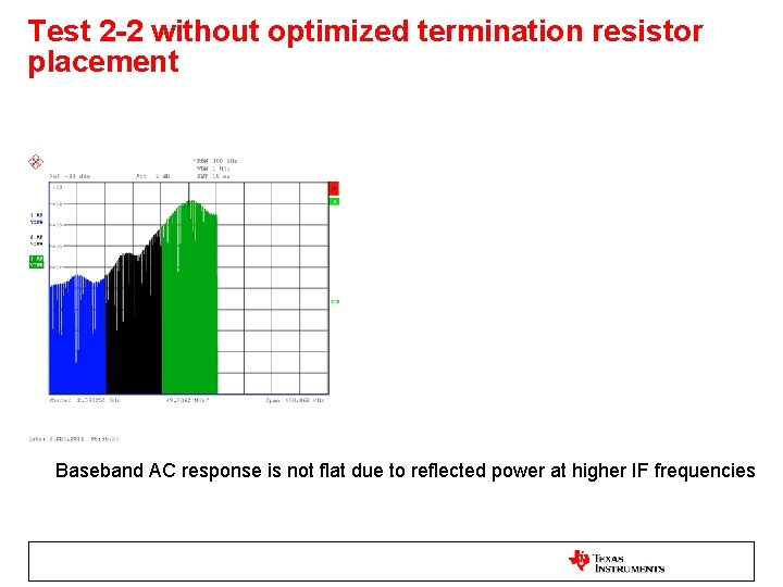
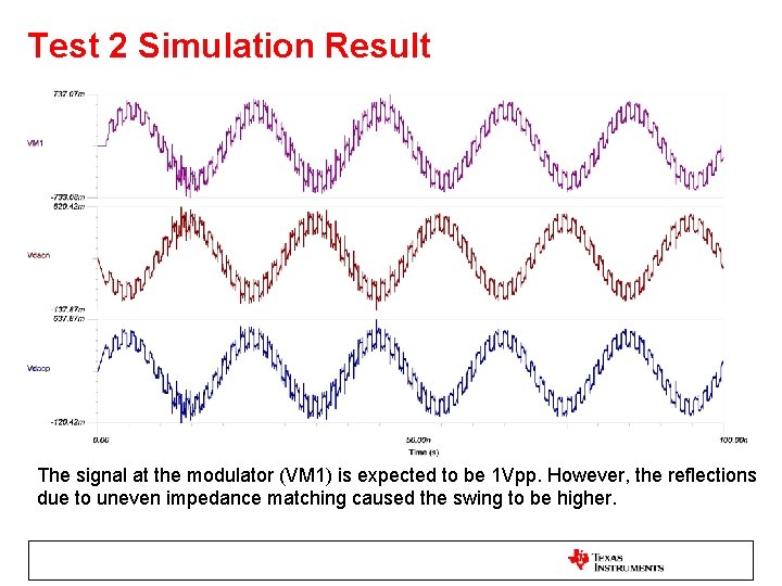
Test 2 -2 without optimized termination resistor placement Baseband AC response is not flat due to reflected power at higher IF frequencies

DAC Output (EVM Top Layer) 1. 2. 3. 4. Keep the differential pair trace (P and N) spacing constant to maintain good impedance matching. On the DAC 3484 EVM, the spacing between Iout. P and Iout. N traces is about 6 mils for a 100 W differential trace. Match trace lengths of the DAC 4 outputs; keep sufficient spacing between the channels to avoid coupling Keep the traces, R, L, and C components symmetric between the I and Q path. Place the DAC 3484, the filter components, and the modulator as compactly as possible. The traces and components should be routed as close to the DAC 3484 and the modulator as possible. TSW 30 H 84 EVM Top Layer shown. IOUT pairs includes: Iout. A 1/2, Iout. B 1/2, Iout. C 1/2, Iout. D 1/2

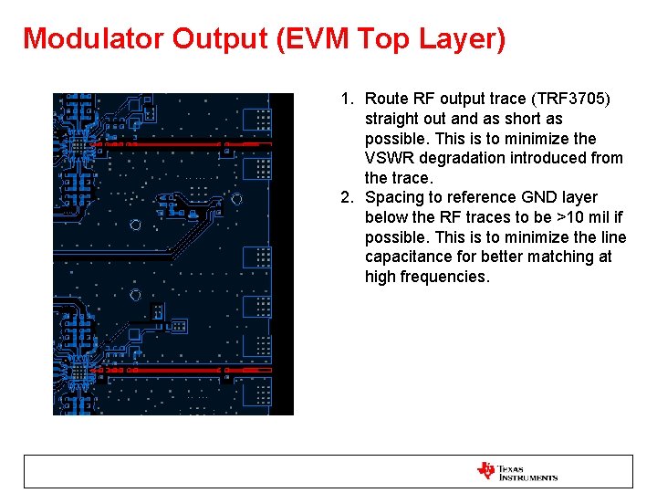
Modulator Output (EVM Top Layer) 1. Route RF output trace (TRF 3705) straight out and as short as possible. This is to minimize the VSWR degradation introduced from the trace. 2. Spacing to reference GND layer below the RF traces to be >10 mil if possible. This is to minimize the line capacitance for better matching at high frequencies.

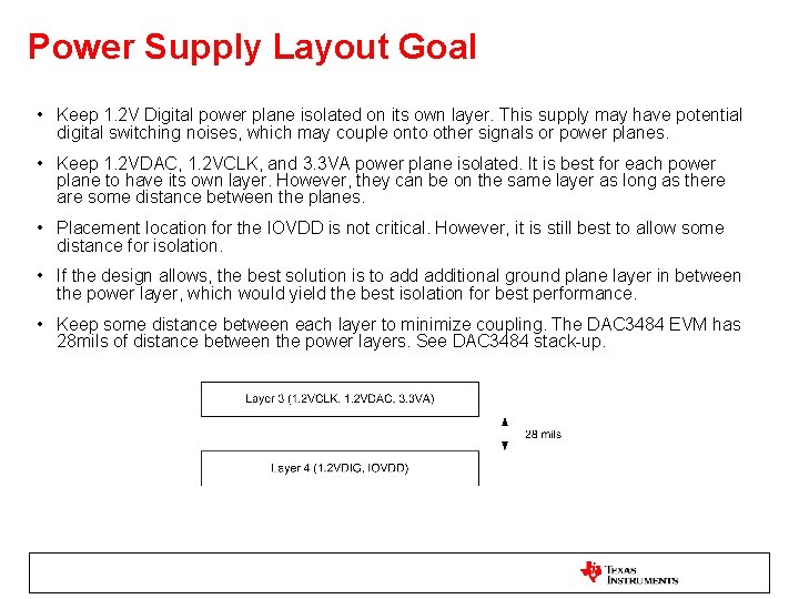
Power Supply Layout Goal • Keep 1. 2 V Digital power plane isolated on its own layer. This supply may have potential digital switching noises, which may couple onto other signals or power planes. • Keep 1. 2 VDAC, 1. 2 VCLK, and 3. 3 VA power plane isolated. It is best for each power plane to have its own layer. However, they can be on the same layer as long as there are some distance between the planes. • Placement location for the IOVDD is not critical. However, it is still best to allow some distance for isolation. • If the design allows, the best solution is to additional ground plane layer in between the power layer, which would yield the best isolation for best performance. • Keep some distance between each layer to minimize coupling. The DAC 3484 EVM has 28 mils of distance between the power layers. See DAC 3484 stack-up.

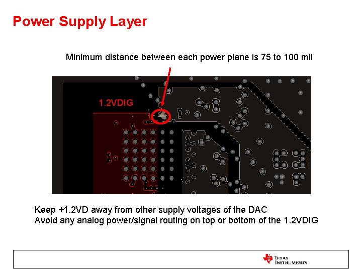
Power Supply Layer Minimum distance between each power plane is 75 to 100 mil 1. 2 VDIG Keep +1. 2 VD away from other supply voltages of the DAC Avoid any analog power/signal routing on top or bottom of the 1. 2 VDIG

Layout - Grounding • Whether to split ground plane into analog and digital, or leave solid – is still a matter of debate – Our position is usually to have one solid, clean ground plane • Then place components and routing over the ground plane with an eye towards return currents – If return currents for digital functions are kept away from analog or other sensitive circuits, then ground plane is already effectively partitioned

Layout – Digital/Analog Grounding • Add the following to the grounding issue. Go through the following mental exercise when working on the layout of a high speed design like this (or, indeed, a high precision lower speed design). Except at one point at the chip where the grounds are connected. “Cut” the ground plane between analog and digital ground making sure all the analog pins are in the analog ground section and all the digital pins are in the digital ground section. Route all the traces without ever crossing the cut. Sometimes this requires moving some other parts around. Once this is done, remove the cuts. The reason for the cuts is just to force the discipline of having all the analog traces stay on their side and all the digital traces stay on their side. • High speed ground currents will run on the ground plane under the traces that sourced the current (i. e. the path of least IMPEDANCE, not RESISTANCE). This is due to the mutual inductances between the trace and ground. Low speed signals will follow the straight line least- resistance path back. At speeds in between the current will have a distribution of paths between the two. What is “high speed” and “low speed” are determined by the geometry and dielectric constants of the materials being used and Maxwell’s equations. • If components are properly placed to make it easier to route all the digital traces away in one direction and all the analog traces in the other direction the currents will never cross or share any common section of the ground plane. You really do not need to know what is high speed and what is low speed to get this right. Just keep in mind the generalities that the current will be distributed between the straight line path of least resistance and the under-the-trace path of least impedance and make sure these return paths for the analog signals run away form the chip in one direction (on one side of the cuts) and the return paths for the digital signals run away from the chip in the other direction (on the other side of the cuts). If this is done right, no current will “want” to cross the cuts and, therefore, the cuts serve no purpose and can be removed, or rather filled in with metal for a solid ground plane. • Once you get good at this thought process there is no need to lay in the temporary cuts. You just place your components and run your traces thinking about what the round trip path is for the currents keeping digital away form analog and it all takes care of itself.

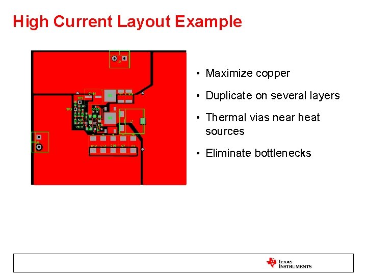
High Current Layout Example • Maximize copper • Duplicate on several layers • Thermal vias near heat sources • Eliminate bottlenecks

Decoupling • Parallel different capacitor types for reduced impedance across a frequency band. • Provide a rapid charge delivery to the IC by using low ESR capacitors placed close to every power and ground pin if possible. • Frequency dependent. • No one size fits all!

Decoupling Recommendations • Create small power planes between IC power pins and decoupling caps instead of traces when there are several caps and power input pins in close proximity. Use as many vias as possible to connect this plane to the internal power plane. • Use the smallest package decoupling capacitors possible (402 footprint) to provide the lowest inductance possible. .

Decoupling Recommendations (cont. ) • Since Decoupling Capacitors cannot provide energy above 150 MHz (at best), Energy for Fast Switching edges is drawn from the capacitance formed by the parallel plates of the power planes in the PCB. • Many PCBs do not have sufficient power plane area to create a capacitor large enough to supply the switching currents required. • Place Power and GND planes as close as possible in board stackup to increase the board capacitance. The closer the better!

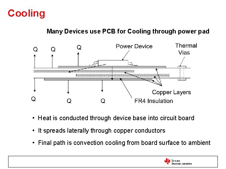
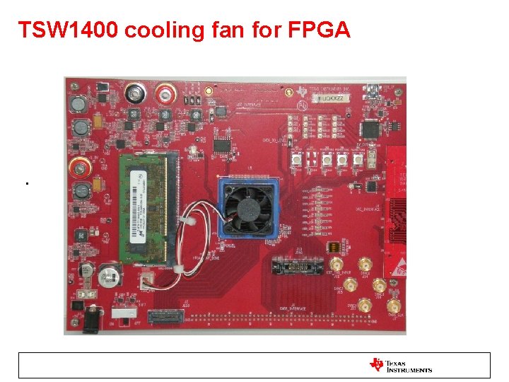
Cooling Many Devices use PCB for Cooling through power pad • Heat is conducted through device base into circuit board • It spreads laterally through copper conductors • Final path is convection cooling from board surface to ambient

PCB Cooling Strategy • Use many large, thick copper planes to distribute heat across PCB surface. • Maximize thermal paths (power pads) with poured copper wherever practical. • Maximize the number of vias inside the power pad. • Use both sides of the board to cool. • Avoid breaks in planes as they substantially degrade lateral heat flow.

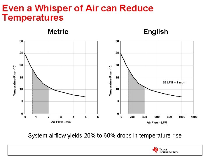
Even a Whisper of Air can Reduce Temperatures Metric English System airflow yields 20% to 60% drops in temperature rise

TSW 1400 cooling fan for FPGA •

Trouble Shooting Help ADC/DAC Spurs & Noise Device Debug

ADC Spurs & Noise • Measure the performance of an ADC using a continuous wave (CW) input. Compare to datasheet performance. • Analyze the ADC output with an ADC capture tool or logic analyzer. • ADC analysis is typically done in the frequency domain by performance a Fast Fourier Transform (FFT) of the ADC output data. • Filter the input signal and CLK as signal generators have very poor distortion leading to large harmonics. • Provide a -1 d. BFS (or 95% of full scale) as the input amplitude input level as most ADC datasheet use this parameters.

ADC Spurs & Noise (cont. ) • Clock spurs – any spurs on the clock input will result in a spur at the ADC output. • The frequency of clock spurs will typically move 1: 1 with the input frequency. If the spur frequency does not change with clock frequency, then the source of the spur is likely coupling into the clock path. • Sub-harmonics on the clock, such as the sample rate divided by 2 or 4 can cause spurs. Sub-harmonics can be generated by clocking devices with multiple outputs and/or divided frequencies. • Coupling between clock paths on the board can be a problem.

ADC Spurs & Noise (cont. ) • Spurious signals that do not move with the input signal are typically generated by some source outside the signal chain and couple into the signal path. • Switching regulators can generate spurs by coupling either through the input path, clock path or the ADC power supplies. • Spurs are at a frequency or offset frequency of several hundred k. Hz. • Switching regulators can be used successfully to power ADCs, but particular care in the interface to the ADC is required.

DAC Spurs & Noise • For the DAC, the test method is the same. Instead of capturing the single tone, the single tone output is generated and capture on the analyzer. • For timing issue with the DAC setup (i. e. setup/hold time), two tone testing or modulating signal testing may show the timing error artifacts better. – The LSBs may not be toggling correctly, but the output single tone may still show correctly because the MSBs are toggling correctly. • The spur location troubleshooting is the same as ADC spur troubleshooting • Verify resistance and dc level on differential baseband signals between DAC and modulators.

Device de-bug • Verify devices have proper input voltages. – If supply is low, verify current spec of regulators. – If not present, check for shorts to GND. • Verify clock integrity, frequency and amplitude. • Verify no solder blobs between pins. • Check for proper solder joints on pins. • Verify internal registers are programmed properly. • Use internal test pattern modes if available (ADC’s). • Verify setup and hold times.

Back Up Material

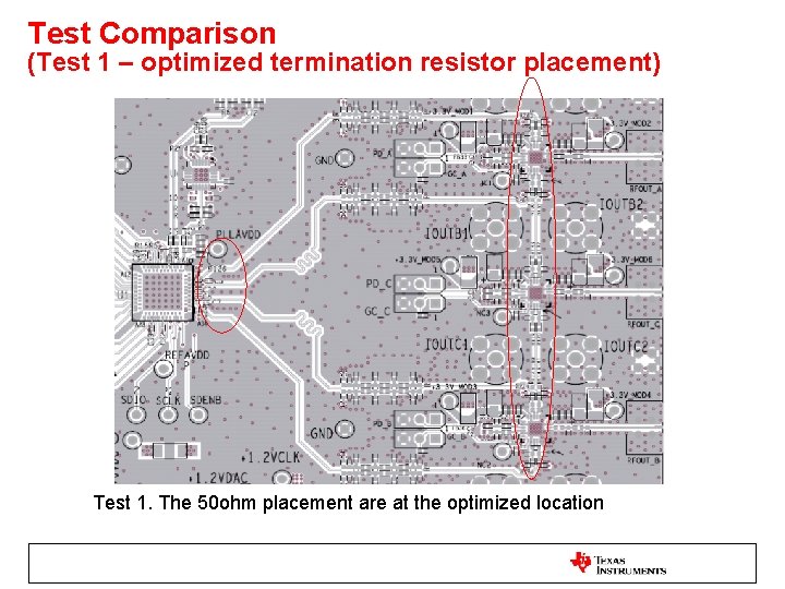
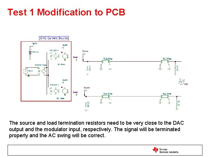
Test Comparison (Test 1 – optimized termination resistor placement) Test 1. The 50 ohm placement are at the optimized location

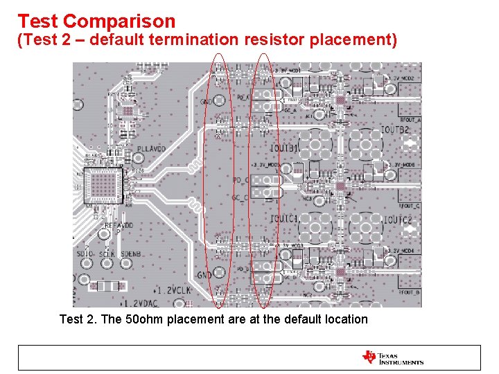
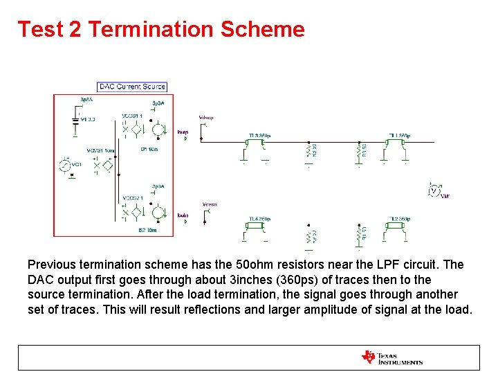
Test Comparison (Test 2 – default termination resistor placement) Test 2. The 50 ohm placement are at the default location

Test 1 Modification to PCB The source and load termination resistors need to be very close to the DAC output and the modulator input, respectively. The signal will be terminated properly and the AC swing will be correct.

Test 1 Simulation Result (Good)

Test 2 Termination Scheme Previous termination scheme has the 50 ohm resistors near the LPF circuit. The DAC output first goes through about 3 inches (360 ps) of traces then to the source termination. After the load termination, the signal goes through another set of traces. This will result reflections and larger amplitude of signal at the load.

Test 2 Simulation Result The signal at the modulator (VM 1) is expected to be 1 Vpp. However, the reflections due to uneven impedance matching caused the swing to be higher.

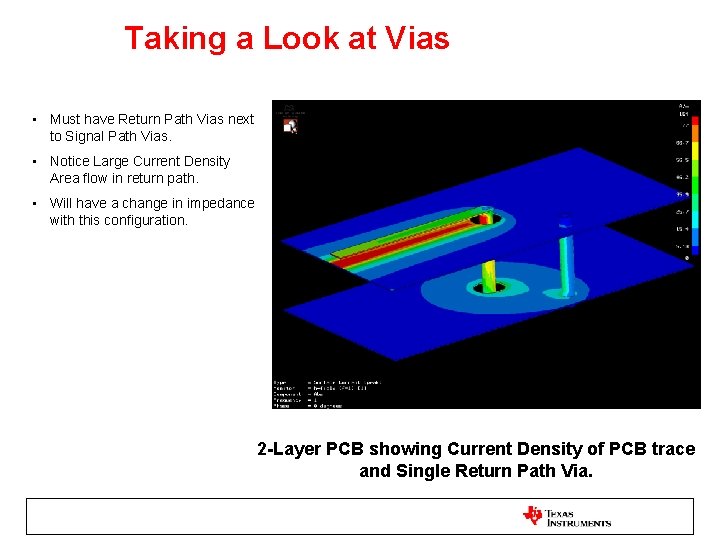
Taking a Look at Vias • Must have Return Path Vias next to Signal Path Vias. • Notice Large Current Density Area flow in return path. • Will have a change in impedance with this configuration. 2 -Layer PCB showing Current Density of PCB trace and Single Return Path Via.

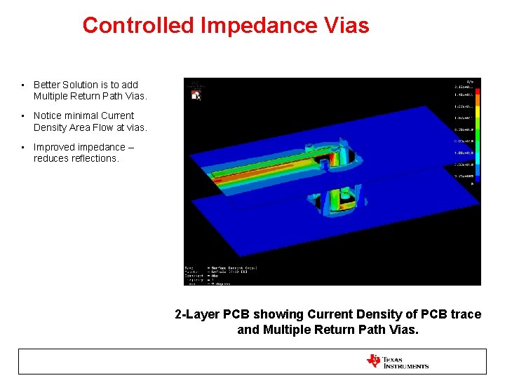
Controlled Impedance Vias • Better Solution is to add Multiple Return Path Vias. • Notice minimal Current Density Area Flow at vias. • Improved impedance – reduces reflections. 2 -Layer PCB showing Current Density of PCB trace and Multiple Return Path Vias.