Switching Power Supply Design EMI Reduction 1 AGENDA
- Slides: 95
Switching Power Supply Design: EMI Reduction 1
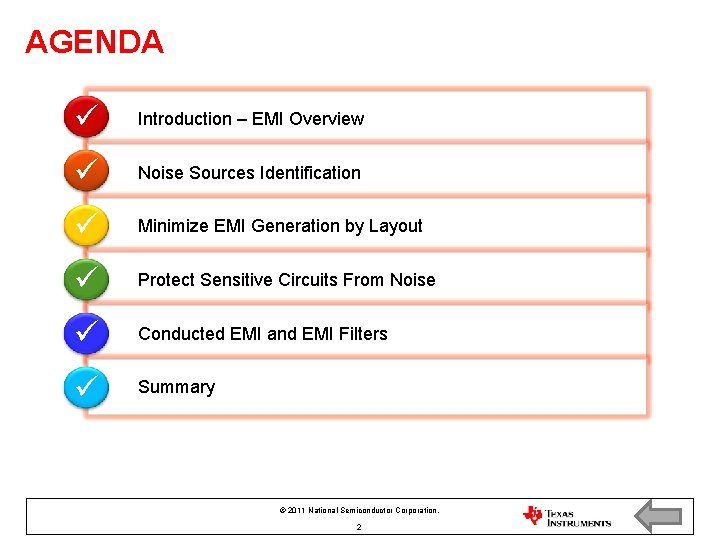
AGENDA Introduction – EMI Overview Noise Sources Identification Minimize EMI Generation by Layout Protect Sensitive Circuits From Noise Conducted EMI and EMI Filters Summary © 2011 National Semiconductor Corporation. 2
AGENDA Introduction – EMI Overview Noise Sources Identification Minimize Noise Generation by Layout Protect Sensitive Circuits from Noise Conducted EMI and EMI Filters Summary • Definition • Standard • EMI in SMPS 3
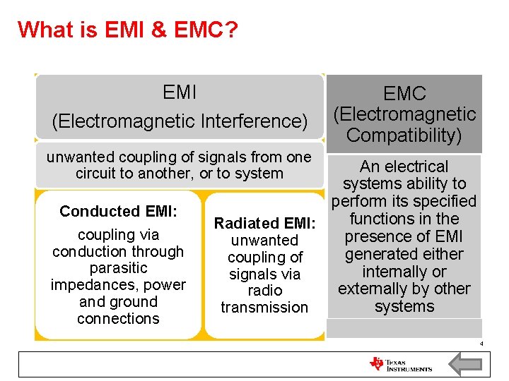
What is EMI & EMC? EMI (Electromagnetic Interference) EMC (Electromagnetic Compatibility) unwanted coupling of signals from one circuit to another, or to system Conducted EMI: coupling via conduction through parasitic impedances, power and ground connections An electrical systems ability to perform its specified functions in the Radiated EMI: presence of EMI unwanted generated either coupling of internally or signals via externally by other radio systems transmission 4
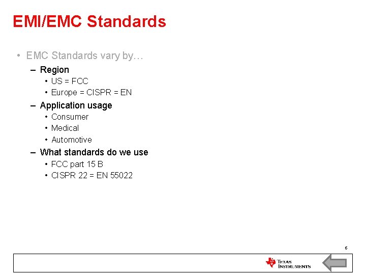
EMI/EMC Standards • EMC Standards vary by… – Region • US = FCC • Europe = CISPR = EN – Application usage • Consumer • Medical • Automotive – What standards do we use • FCC part 15 B • CISPR 22 = EN 55022 5
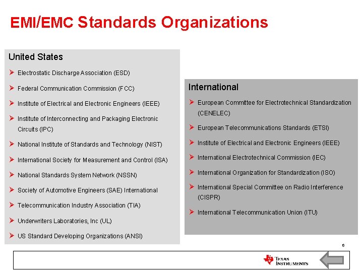
EMI/EMC Standards Organizations United States Ø Electrostatic Discharge Association (ESD) Ø Federal Communication Commission (FCC) International Ø Institute of Electrical and Electronic Engineers (IEEE) Ø European Committee for Electrotechnical Standardization Ø Institute of Interconnecting and Packaging Electronic Circuits (IPC) (CENELEC) Ø European Telecommunications Standards (ETSI) Ø National Institute of Standards and Technology (NIST) Ø Institute of Electrical and Electronic Engineers (IEEE) Ø International Society for Measurement and Control (ISA) Ø International Electrotechnical Commission (IEC) Ø National Standards System Network (NSSN) Ø International Organization for Standardization (ISO) Ø Society of Automotive Engineers (SAE) International Ø International Special Committee on Radio Interference (CISPR) Ø Telecommunication Industry Association (TIA) Ø International Telecommunication Union (ITU) Ø Underwriters Laboratories, Inc (UL) Ø US Standard Developing Organizations (ANSI) 6
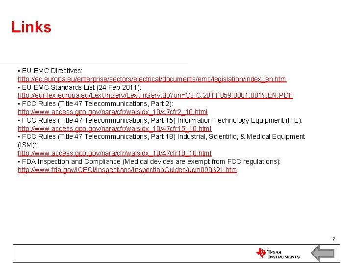
Links • EU EMC Directives: http: //ec. europa. eu/enterprise/sectors/electrical/documents/emc/legislation/index_en. htm • EU EMC Standards List (24 Feb 2011): http: //eur-lex. europa. eu/Lex. Uri. Serv. do? uri=OJ: C: 2011: 059: 0001: 0019: EN: PDF • FCC Rules (Title 47 Telecommunications, Part 2): http: //www. access. gpo. gov/nara/cfr/waisidx_10/47 cfr 2_10. html • FCC Rules (Title 47 Telecommunications, Part 15) Information Technology Equipment (ITE): http: //www. access. gpo. gov/nara/cfr/waisidx_10/47 cfr 15_10. html • FCC Rules (Title 47 Telecommunications, Part 18) Industrial, Scientific, & Medical Equipment (ISM): http: //www. access. gpo. gov/nara/cfr/waisidx_10/47 cfr 18_10. html • FDA Inspection and Compliance (Medical devices are exempt from FCC regulations): http: //www. fda. gov/ICECI/Inspections/Inspection. Guides/ucm 090621. htm 7
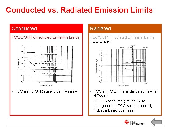
Conducted vs. Radiated Emission Limits Conducted Radiated FCC/CISPR Conducted Emission Limits FCC/CISPR Radiated Emission Limits Measured at 10 m • FCC and CISPR standards the same • FCC and CISPR standards somewhat different • FCC B (consumer) much more stringent than FCC A (commercial, industrial, and business) 8
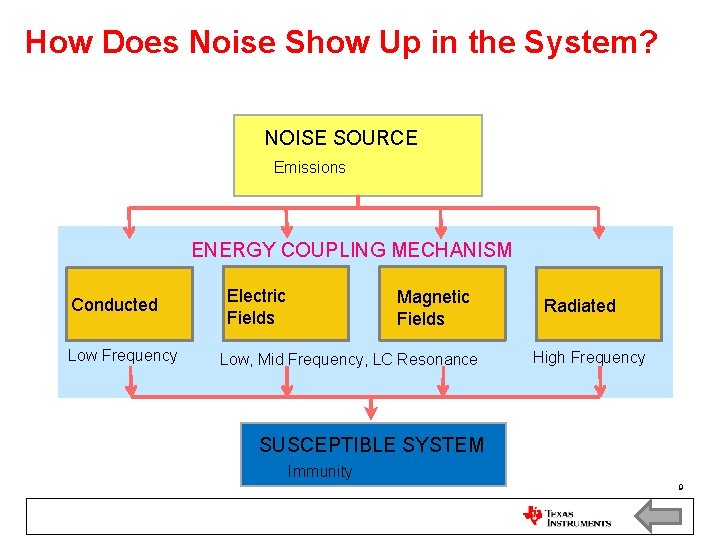
How Does Noise Show Up in the System? NOISE SOURCE Emissions ENERGY COUPLING MECHANISM Conducted Low Frequency Electric Fields Magnetic Fields Low, Mid Frequency, LC Resonance Radiated High Frequency SUSCEPTIBLE SYSTEM Immunity 9
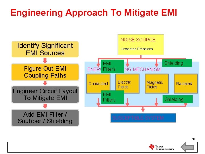
Engineering Approach To Mitigate EMI NOISE SOURCE Identify Significant EMI Sources Figure Out EMI Coupling Paths Unwanted Emissions Shielding EMI Filters ENERGY COUPLING MECHANISM Electric Fields Conducted Engineer Circuit Layout To Mitigate EMI Add EMI Filter / Snubber / Shielding Magnetic Fields EMI Filters Radiated Shielding SUSCEPTIBLE SYSTEM 10
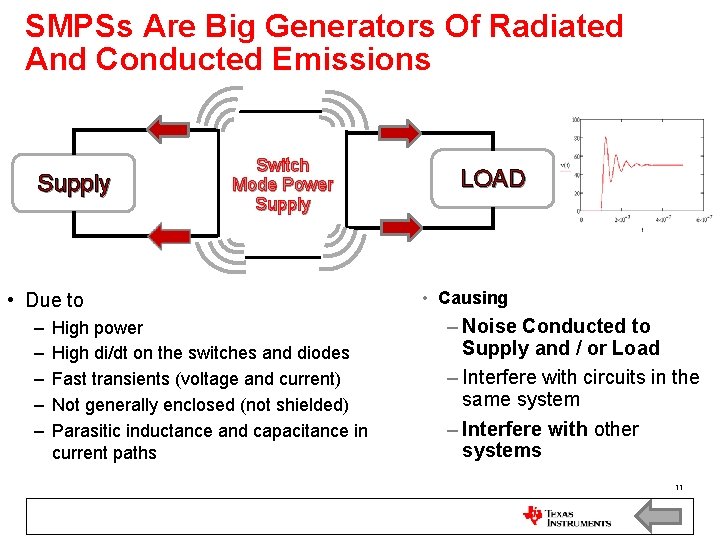
SMPSs Are Big Generators Of Radiated And Conducted Emissions Supply Switch Mode Power Supply • Due to – – – High power High di/dt on the switches and diodes Fast transients (voltage and current) Not generally enclosed (not shielded) Parasitic inductance and capacitance in current paths LOAD • Causing – Noise Conducted to Supply and / or Load – Interfere with circuits in the same system – Interfere with other systems 11
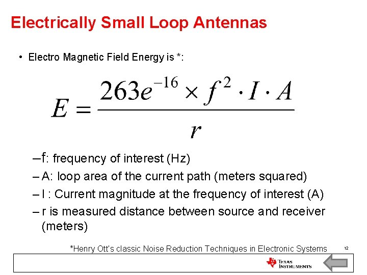
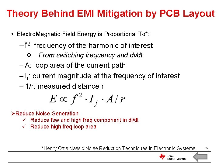
Electrically Small Loop Antennas • Electro Magnetic Field Energy is *: – f: frequency of interest (Hz) – A: loop area of the current path (meters squared) – I : Current magnitude at the frequency of interest (A) – r is measured distance between source and receiver (meters) *Henry Ott’s classic Noise Reduction Techniques in Electronic Systems 12
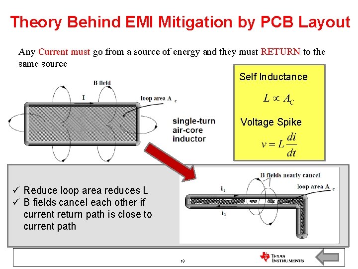
Theory Behind EMI Mitigation by PCB Layout Any Current must go from a source of energy and they must RETURN to the same source Self Inductance Voltage Spike Reduce loop area reduces L B fields cancel each other if current return path is close to current path 13 13
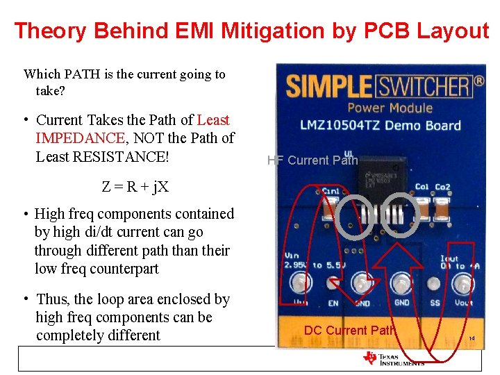
Theory Behind EMI Mitigation by PCB Layout Which PATH is the current going to take? • Current Takes the Path of Least IMPEDANCE, NOT the Path of Least RESISTANCE! HF Current Path Z = R + j. X • High freq components contained by high di/dt current can go through different path than their low freq counterpart • Thus, the loop area enclosed by high freq components can be completely different DC Current Path 14
Theory Behind EMI Mitigation by PCB Layout • Electro. Magnetic Field Energy is Proportional To*: – f 2: frequency of the harmonic of interest v From switching frequency and di/dt – A: loop area of the current path – If: current magnitude at the frequency of interest – 1/r: measured distance r ØReduce Noise Generation Reduce fsw and high freq component in di/dt Reduce high freq loop area *Henry Ott’s classic Noise Reduction Techniques in Electronic Systems 15
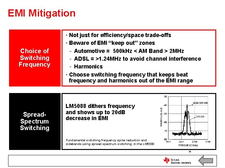
EMI Mitigation Choice of Switching Frequency Spread. Spectrum Switching • Not just for efficiency/space trade-offs • Beware of EMI “keep out” zones - Automotive = 500 k. Hz < AM Band > 2 MHz - ADSL = >1. 24 MHz to avoid channel interference - Harmonics • Choose switching frequency that keeps beat frequency and harmonics out of the EMI range LM 5088 dithers frequency and shows up to 20 d. B decrease in EMI Fundamental switching frequency spike reduction and sidebands using spread spectrum switching in the LM 5088 16
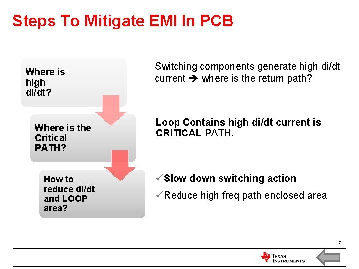
Steps To Mitigate EMI In PCB Where is high di/dt? Where is the Critical PATH? How to reduce di/dt and LOOP area? Switching components generate high di/dt current where is the return path? Loop Contains high di/dt current is CRITICAL PATH. Slow down switching action Reduce high freq path enclosed area 17
AGENDA EMI Overview – definition and standards Noise Sources Identification Minimize EMI Generation by Layout Protect Sensitive Circuits from Noise Conducted EMI and EMI Filters Summary Isolated and High Power Density Power Supply Board • Buck • Boost • Buck Boost 18
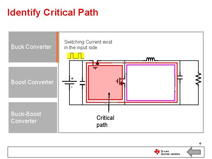
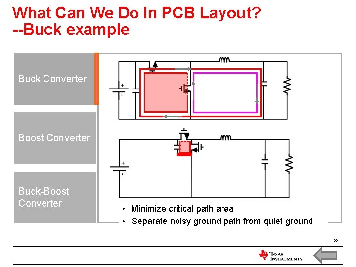
Identify Critical Path Buck Converter Switching Current exist in the input side Boost Converter Buck-Boost Converter Critical path 19
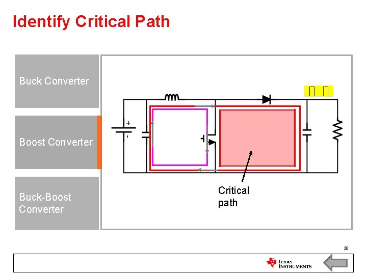
Identify Critical Path Buck Converter Boost Converter Buck-Boost Converter Critical path 20
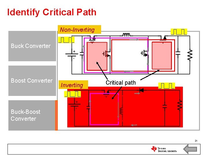
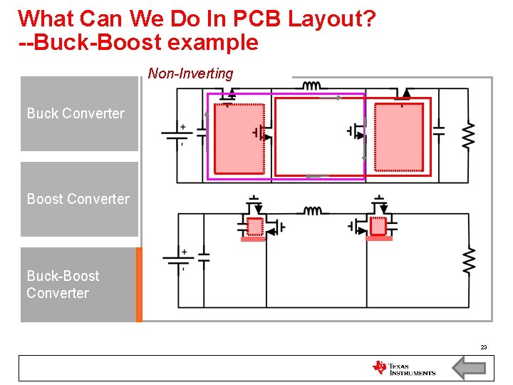
Identify Critical Path Non-Inverting Buck Converter Boost Converter Inverting Critical path Buck-Boost Converter 21
What Can We Do In PCB Layout? --Buck example Buck Converter Boost Converter Buck-Boost Converter • Minimize critical path area • Separate noisy ground path from quiet ground 22
What Can We Do In PCB Layout? --Buck-Boost example Non-Inverting Buck Converter Boost Converter Buck-Boost Converter 23
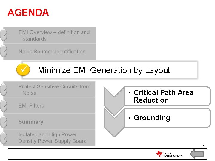
AGENDA Minimize EMI Generation by Layout • Critical Path Area Reduction • Grounding 24
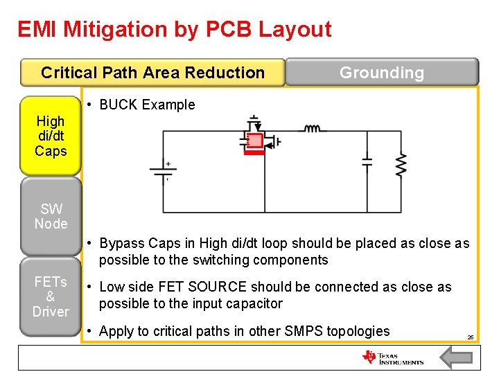
EMI Mitigation by PCB Layout Critical Path Area Reduction Grounding • BUCK Example High di/dt Caps SW Node • Bypass Caps in High di/dt loop should be placed as close as possible to the switching components FETs & Driver • Low side FET SOURCE should be connected as close as possible to the input capacitor • Apply to critical paths in other SMPS topologies 25
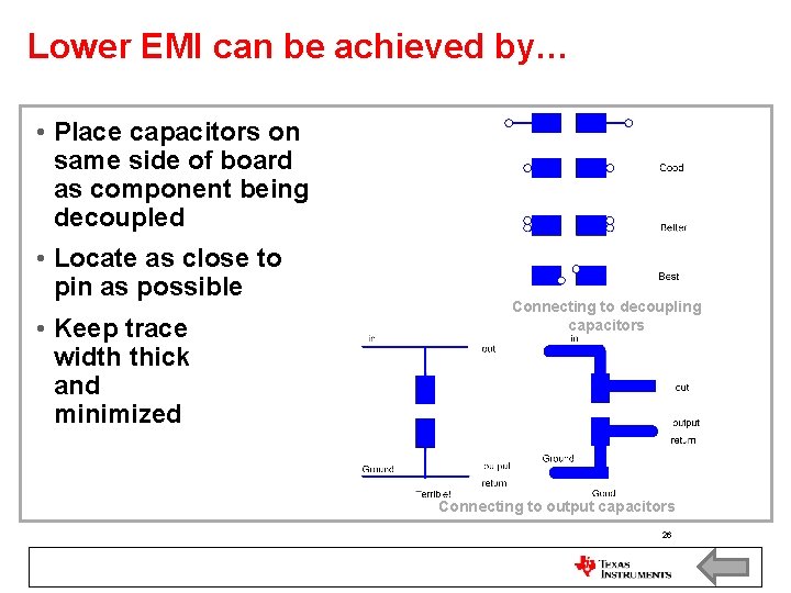
Lower EMI can be achieved by… • Place capacitors on same side of board as component being decoupled • Locate as close to pin as possible • Keep trace width thick and minimized Connecting to decoupling capacitors Connecting to output capacitors 26
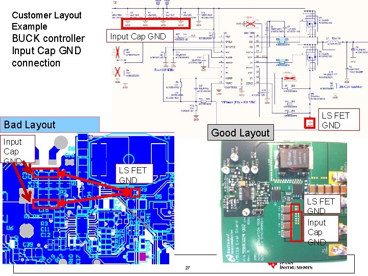
Customer Layout Example BUCK controller Input Cap GND connection Input Cap GND Bad Layout Input Cap GND Good Layout LS FET GND Input Cap GND 27
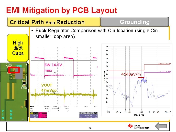
EMI Mitigation by PCB Layout Grounding Critical Path Area Reduction • Buck Regulator Comparison with Cin location (single Cin, smaller loop area) High di/dt Caps SW Node SW 14. 5 V max 41 d. BµV/m VOUT 47 m. Vpp FETs & Driver VIN VOUT 28 28
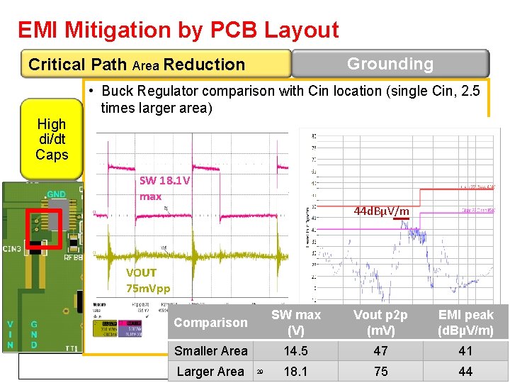
EMI Mitigation by PCB Layout Grounding Critical Path Area Reduction • Buck Regulator comparison with Cin location (single Cin, 2. 5 times larger area) High di/dt Caps SW 18. 1 V max 44 d. BµV/m SW Node FETs & Driver VOUT 75 m. Vpp Comparison SW max (V) Vout p 2 p (m. V) EMI peak (d. BµV/m) Smaller Area 14. 5 47 41 18. 1 75 44 Larger Area 29 29
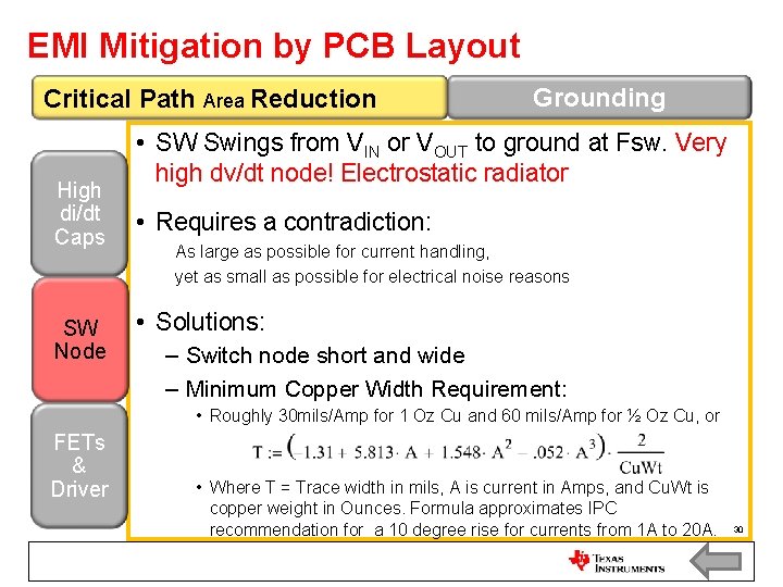
EMI Mitigation by PCB Layout Critical Path Area Reduction High di/dt Caps SW Node Grounding • SW Swings from VIN or VOUT to ground at Fsw. Very high dv/dt node! Electrostatic radiator • Requires a contradiction: As large as possible for current handling, yet as small as possible for electrical noise reasons • Solutions: – Switch node short and wide – Minimum Copper Width Requirement: • Roughly 30 mils/Amp for 1 Oz Cu and 60 mils/Amp for ½ Oz Cu, or FETs & Driver • Where T = Trace width in mils, A is current in Amps, and Cu. Wt is copper weight in Ounces. Formula approximates IPC recommendation for a 10 degree rise for currents from 1 A to 20 A. 30
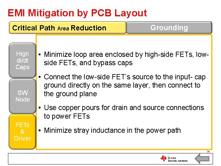
EMI Mitigation by PCB Layout Critical Path Area Reduction Grounding • Minimize loop area enclosed by high-side FETs, lowside FETs, and bypass caps • Connect the low-side FET’s source to the input- cap ground directly on the same layer, then connect to the ground plane • Use copper pours for drain and source connections to power FETs • Minimize stray inductance in the power path 31
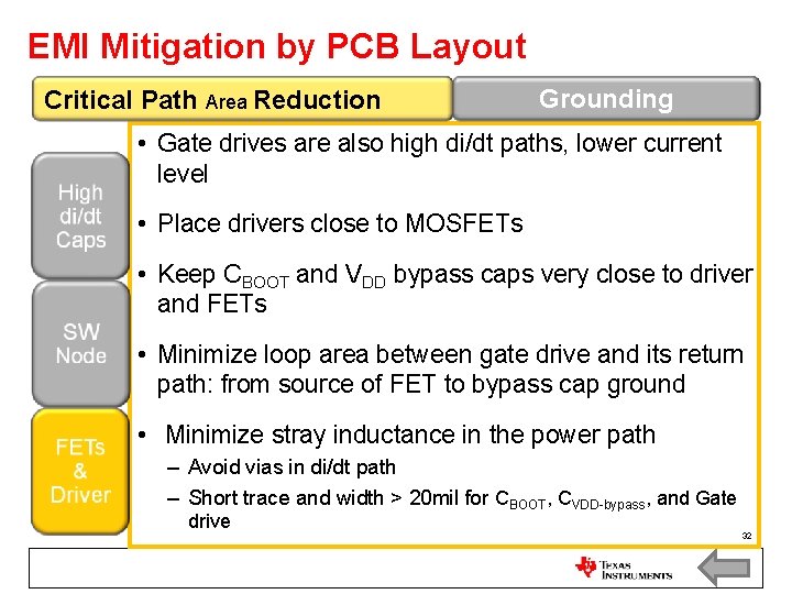
EMI Mitigation by PCB Layout Critical Path Area Reduction Grounding • Gate drives are also high di/dt paths, lower current level • Place drivers close to MOSFETs • Keep CBOOT and VDD bypass caps very close to driver and FETs • Minimize loop area between gate drive and its return path: from source of FET to bypass cap ground • Minimize stray inductance in the power path – Avoid vias in di/dt path – Short trace and width > 20 mil for CBOOT, CVDD-bypass, and Gate drive 32
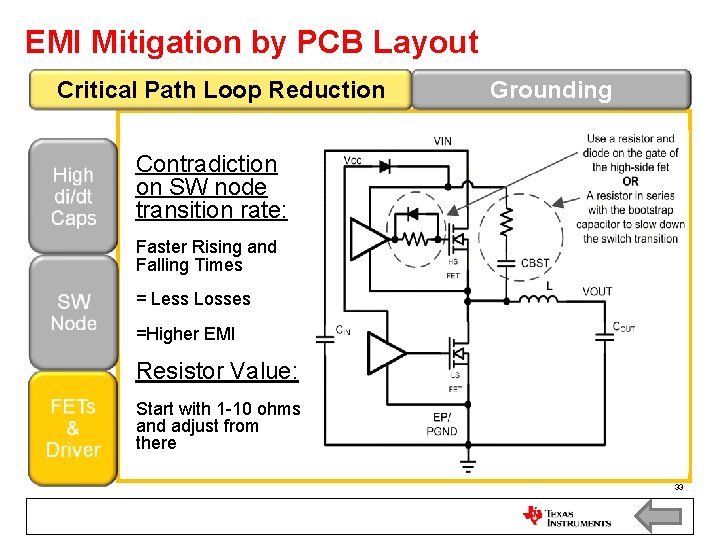
EMI Mitigation by PCB Layout Critical Path Loop Reduction Grounding Contradiction on SW node transition rate: Faster Rising and Falling Times = Less Losses =Higher EMI Resistor Value: Start with 1 -10 ohms and adjust from there 33
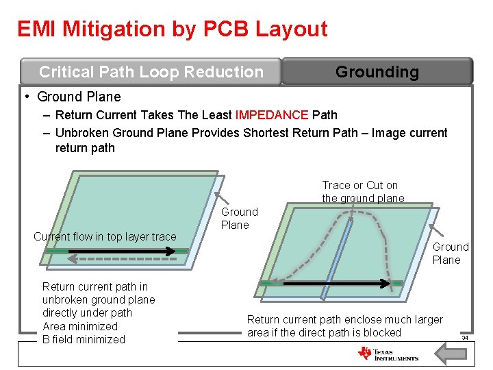
EMI Mitigation by PCB Layout Critical Path Loop Reduction Grounding • Ground Plane – Return Current Takes The Least IMPEDANCE Path – Unbroken Ground Plane Provides Shortest Return Path – Image current return path Trace or Cut on the ground plane Current flow in top layer trace Return current path in unbroken ground plane directly under path Area minimized B field minimized Ground Plane Return current path enclose much larger area if the direct path is blocked 34
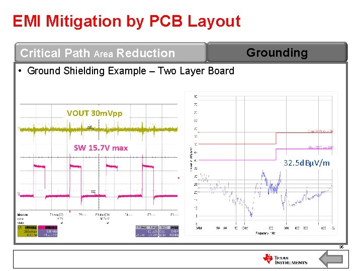
EMI Mitigation by PCB Layout Critical Path Area Reduction Grounding • Ground Shielding Example – Two Layer Board VOUT 30 m. Vpp SW 15. 7 V max 32. 5 d. BμV/m 35
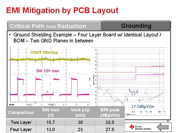
EMI Mitigation by PCB Layout Grounding Critical Path Area Reduction • Ground Shielding Example – Four Layer Board w/ Identical Layout / BOM – Two GND Planes in between VOUT 23 m. Vpp SW 13 V max Comparison SW max (V) Vout p 2 p (m. V) EMI peak (d. BµV/m) Two Layer 15. 7 30 32. 5 Four Layer 13. 0 23 27. 5 d. BμV/m 36
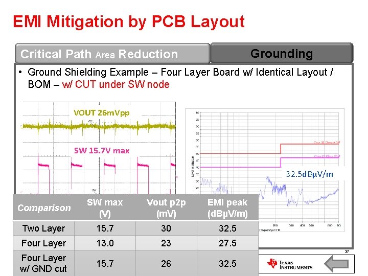
EMI Mitigation by PCB Layout Grounding Critical Path Area Reduction • Ground Shielding Example – Four Layer Board w/ Identical Layout / BOM – w/ CUT under SW node VOUT 26 m. Vpp SW 15. 7 V max 32. 5 d. BμV/m Comparison SW max (V) Vout p 2 p (m. V) EMI peak (d. BµV/m) Two Layer 15. 7 30 32. 5 Four Layer 13. 0 23 27. 5 Four Layer w/ GND cut 37 15. 7 26 32. 5
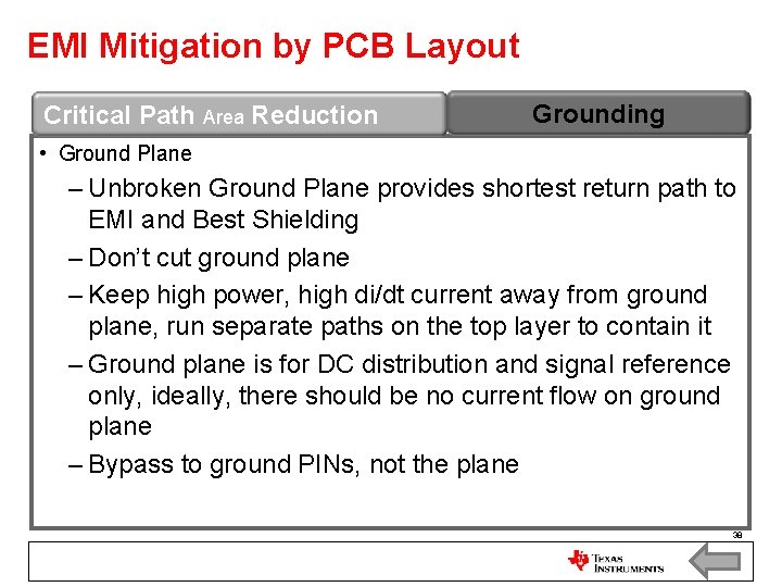
EMI Mitigation by PCB Layout Critical Path Area Reduction Grounding • Ground Plane – Unbroken Ground Plane provides shortest return path to EMI and Best Shielding – Don’t cut ground plane – Keep high power, high di/dt current away from ground plane, run separate paths on the top layer to contain it – Ground plane is for DC distribution and signal reference only, ideally, there should be no current flow on ground plane – Bypass to ground PINs, not the plane 38
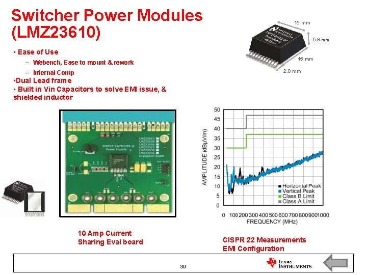
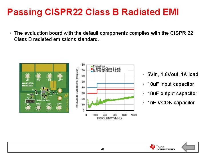
Switcher Power Modules (LMZ 23610) • Ease of Use 15 mm 5. 9 mm 15 mm – Webench, Ease to mount & rework 2. 8 mm – Internal Comp • Dual Lead frame • Built in Vin Capacitors to solve EMI issue, & shielded inductor 10 Amp Current Sharing Eval board CISPR 22 Measurements EMI Configuration 39
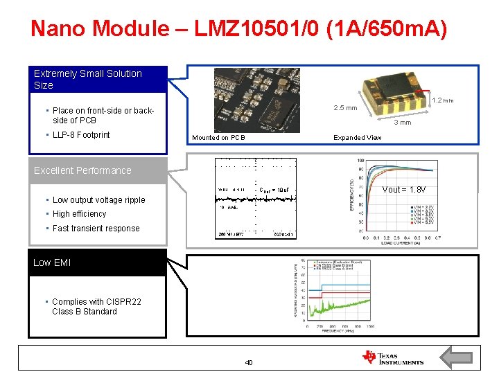
Nano Module – LMZ 10501/0 (1 A/650 m. A) Extremely Small Solution Size • Place on front-side or backside of PCB • LLP-8 Footprint 1. 2 mm 2. 5 mm 3 mm Mounted on PCB Expanded View Excellent Performance COUT = 10 u. F • Low output voltage ripple • High efficiency • Fast transient response Low EMI • Complies with CISPR 22 Class B Standard 40 Vout = 1. 8 V
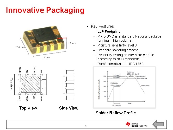
Innovative Packaging • Key Features: – LLP Footprint – Micro SMD is a standard National package running in high volume – Moisture sensitivity level 3 – Standard soldering process – Reliability testing on complete module according to NSC standards – Ro. HS compliance to IPC 1752 1. 2 mm 2. 5 mm 3 mm Top View Side View Solder Reflow Profile 41
Passing CISPR 22 Class B Radiated EMI • The evaluation board with the default components complies with the CISPR 22 Class B radiated emissions standard. • 5 Vin, 1. 8 Vout, 1 A load • 10 u. F input capacitor • 10 u. F output capacitor • 1 n. F VCON capacitor 42
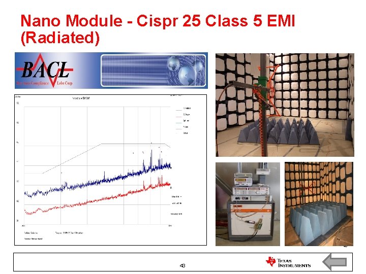
Nano Module - Cispr 25 Class 5 EMI (Radiated) 43 43
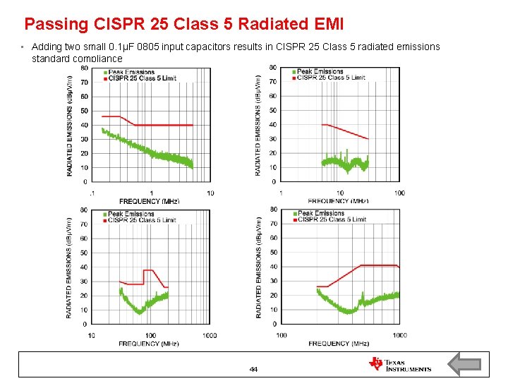
Passing CISPR 25 Class 5 Radiated EMI • Adding two small 0. 1μF 0805 input capacitors results in CISPR 25 Class 5 radiated emissions standard compliance 44
AGENDA Protect Sensitive Circuits from Noise 45
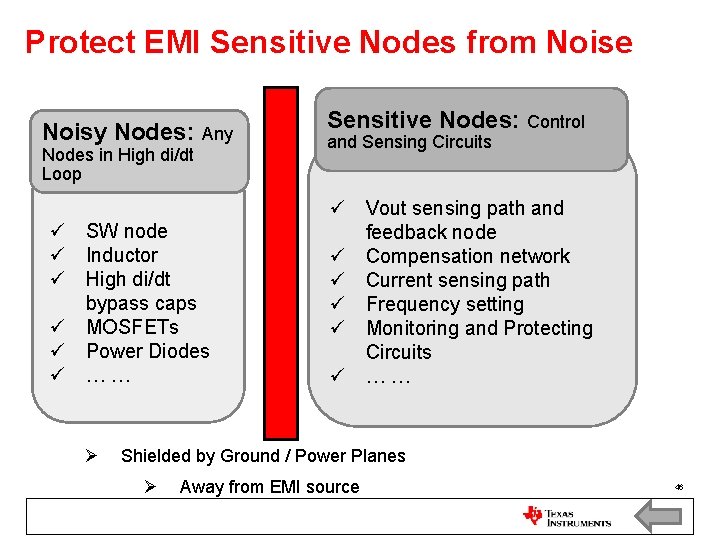
Protect EMI Sensitive Nodes from Noise Noisy Nodes: Any Nodes in High di/dt Loop SW node Inductor High di/dt bypass caps MOSFETs Power Diodes …… Ø Sensitive Nodes: Control and Sensing Circuits Vout sensing path and feedback node Compensation network Current sensing path Frequency setting Monitoring and Protecting Circuits …… Shielded by Ground / Power Planes Ø Away from EMI source 46
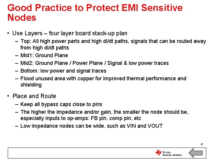
Good Practice to Protect EMI Sensitive Nodes • Use Layers – four layer board stack-up plan – Top: All high power parts and high di/dt paths, signals that can be routed away from high di/dt paths – Mid 1: Ground Plane – Mid 2: Ground Plane / Power Plane / Signal & low power traces – Bottom: low power and signal traces – Flood unused area with copper for improved thermal performance and shielding • Place and Route – Keep all bypass caps close to pins – The higher the impedance and/or gain, the smaller the node should be, especially inputs to op-amps: FB pin, comp pin, etc – Low impedance nodes can be wide, such as VIN and VOUT 47
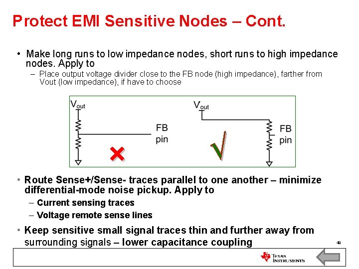
Protect EMI Sensitive Nodes – Cont. • Make long runs to low impedance nodes, short runs to high impedance nodes. Apply to – Place output voltage divider close to the FB node (high impedance), farther from Vout (low impedance), if have to choose × √ • Route Sense+/Sense- traces parallel to one another – minimize differential-mode noise pickup. Apply to – Current sensing traces – Voltage remote sense lines • Keep sensitive small signal traces thin and further away from surrounding signals – lower capacitance coupling 48
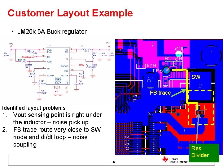
Customer Layout Example • LM 20 k 5 A Buck regulator SW FB trace L Identified layout problems 1. Vout sensing point is right under the inductor – noise pick up 2. FB trace route very close to SW node and di/dt loop – noise coupling Res 49 Divider 49
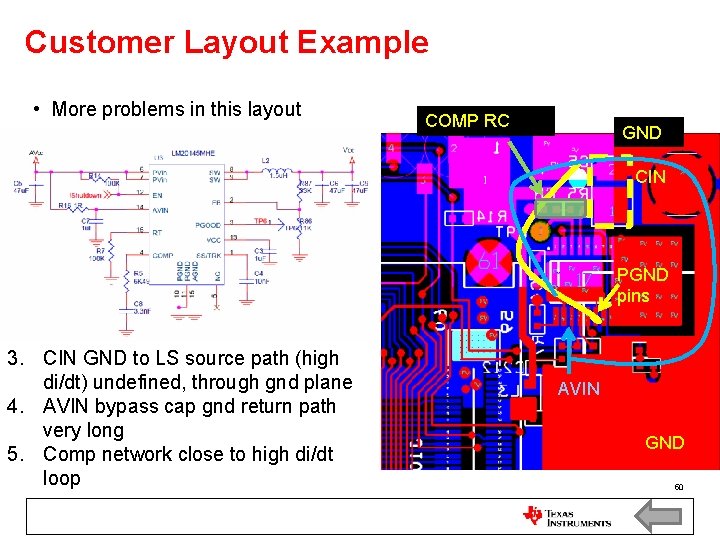
Customer Layout Example • More problems in this layout COMP RC GND CIN PGND pins 3. CIN GND to LS source path (high di/dt) undefined, through gnd plane 4. AVIN bypass cap gnd return path very long 5. Comp network close to high di/dt loop AVIN GND 50
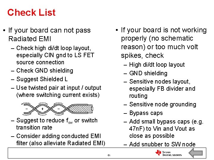
Check List • If your board is not working properly (no schematic reason) or too much volt spikes, check • If your board can not pass Radiated EMI – Check high di/dt loop layout, especially CIN gnd to LS FET source connection – Check GND shielding – Suggest Shielded L – Use twisted pair at input / output (where switching current exists) – High di/dt loop layout – GND shielding – Sensitive nodes layout, especially FB divider and routing – Sensitive node grounding – Bypass caps – Add small bypass caps (e. g. 47 n. F) to Vin and Vout as close as possible – Add snubber to SW node – Suggest to reduce fsw or switch transition rate – Consider adding conducted EMI filter (also alleviate Radiated EMI) 51
AGENDA Conducted EMI and EMI Filters 52
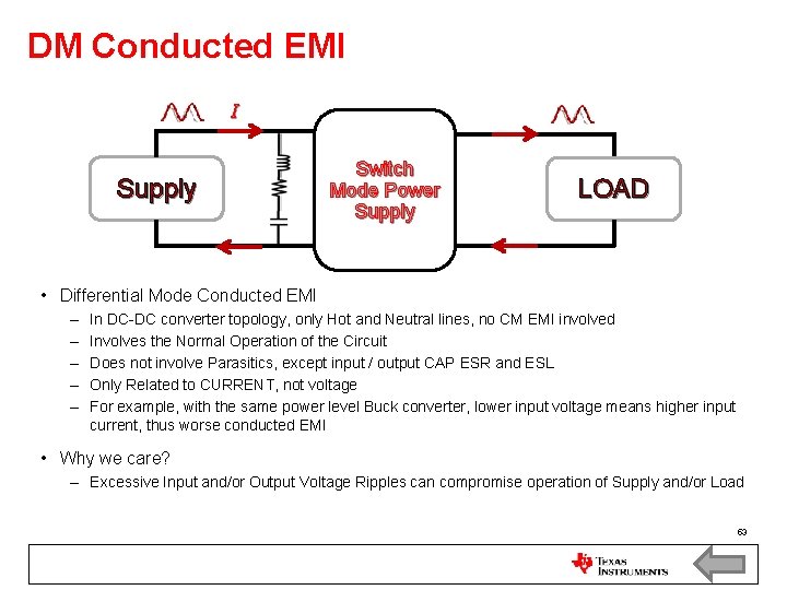
DM Conducted EMI I Supply Switch Mode Power Supply LOAD • Differential Mode Conducted EMI – – – In DC-DC converter topology, only Hot and Neutral lines, no CM EMI involved Involves the Normal Operation of the Circuit Does not involve Parasitics, except input / output CAP ESR and ESL Only Related to CURRENT, not voltage For example, with the same power level Buck converter, lower input voltage means higher input current, thus worse conducted EMI • Why we care? – Excessive Input and/or Output Voltage Ripples can compromise operation of Supply and/or Load 53
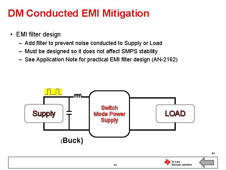
DM Conducted EMI Mitigation • EMI filter design – Add filter to prevent noise conducted to Supply or Load – Must be designed so it does not affect SMPS stability – See Application Note for practical EMI filter design (AN-2162) Switch Mode Power Supply LOAD (Buck) 54 54
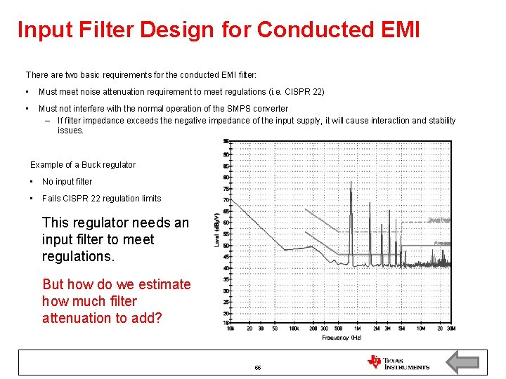
Input Filter Design for Conducted EMI There are two basic requirements for the conducted EMI filter: • Must meet noise attenuation requirement to meet regulations (i. e. CISPR 22) • Must not interfere with the normal operation of the SMPS converter – If filter impedance exceeds the negative impedance of the input supply, it will cause interaction and stability issues. Example of a Buck regulator • No input filter • Fails CISPR 22 regulation limits This regulator needs an input filter to meet regulations. But how do we estimate how much filter attenuation to add? 55
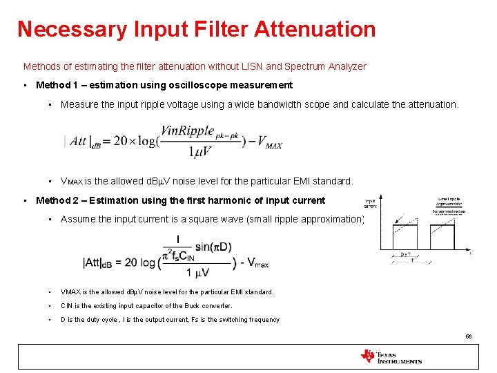
Necessary Input Filter Attenuation Methods of estimating the filter attenuation without LISN and Spectrum Analyzer • Method 1 – estimation using oscilloscope measurement • Measure the input ripple voltage using a wide bandwidth scope and calculate the attenuation. • VMAX is the allowed d. BμV noise level for the particular EMI standard. • Method 2 – Estimation using the first harmonic of input current • Assume the input current is a square wave (small ripple approximation) • VMAX is the allowed d. BμV noise level for the particular EMI standard. • CIN is the existing input capacitor of the Buck converter. • D is the duty cycle , I is the output current, Fs is the switching frequency 56
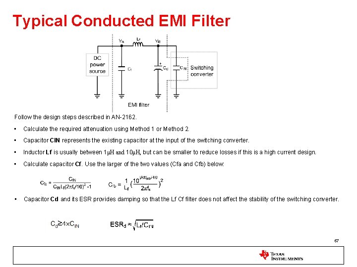
Typical Conducted EMI Filter Follow the design steps described in AN-2162. • Calculate the required attenuation using Method 1 or Method 2. • Capacitor CIN represents the existing capacitor at the input of the switching converter. • Inductor Lf is usually between 1μH and 10μH, but can be smaller to reduce losses if this is a high current design. • Calculate capacitor Cf. Use the larger of the two values (Cfa and Cfb) below: • Capacitor Cd and its ESR provides damping so that the Lf Cf filter does not affect the stability of the switching converter. 57
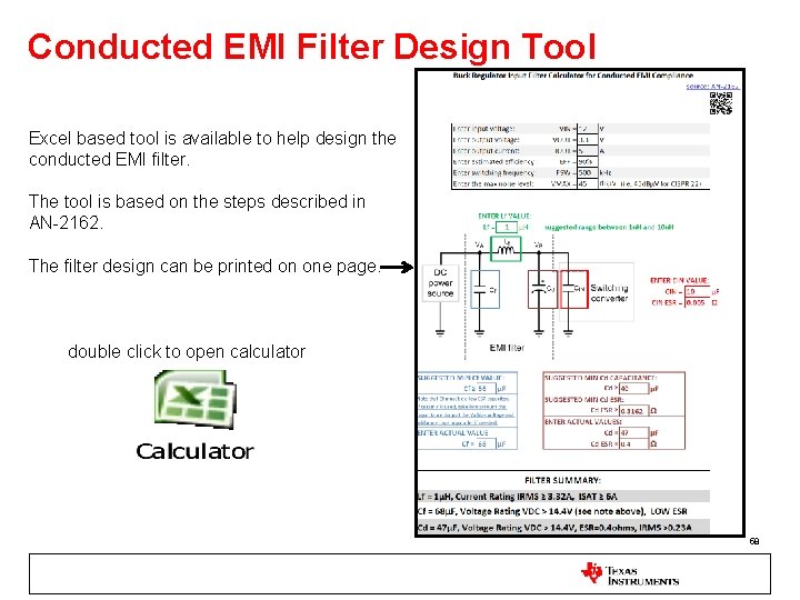
Conducted EMI Filter Design Tool Excel based tool is available to help design the conducted EMI filter. The tool is based on the steps described in AN-2162. The filter design can be printed on one page. double click to open calculator 58
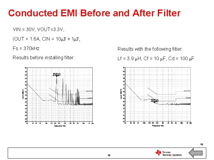
Conducted EMI Before and After Filter VIN = 30 V, VOUT=3. 3 V, IOUT = 1. 6 A, CIN = 10μF + 1μF, Fs = 370 k. Hz Results with the following filter: Results before installing filter: Lf = 3. 9 μH, Cf = 10 μF, Cd = 100 μF 59 59
AGENDA EMI Overview – definition and standards Noise Sources Identification Minimize EMI Generation by Layout Protect Sensitive Circuits from Noise Conducted EMI and EMI Filters Summary 60
SUMMARY • EMI is Electromagnetic Interference. There are many EMC standards, based on regions and applications • SMPSs are big source of radiated and conducted EMI • EMI comes from high power switching action • EMI problems can be mitigated by identifying high di/dt loop and reducing loop area by careful board layout • Sensitive circuits should be protected with careful layout and shielding • Filters can be designed to attenuate conducted EMI to protect supply / Load • Filters also help reduce radiated EMI 61
AGENDA Questions 62
Isolated and High Power Density Power Supply Board Youhao Xi Phoenix Design Center April 2011 63
Outline • Identify critical paths in isolated power circuits • Considerations for high power density board layout: copper layer thickness, trace width, and trace spacing and width • The isolation boundary • PCB Heat-sink • An isolated power supply example • Summary 64
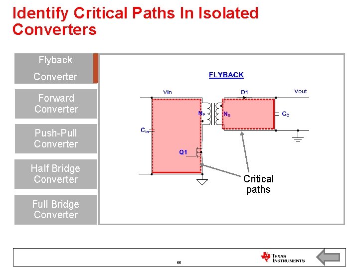
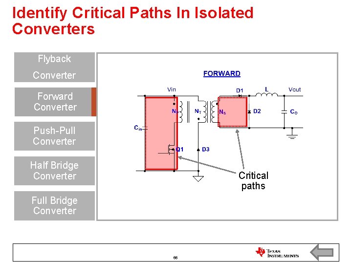
Identify Critical Paths In Isolated Converters Flyback Converter Forward Converter Push-Pull Converter Half Bridge Converter Critical paths Full Bridge Converter 65
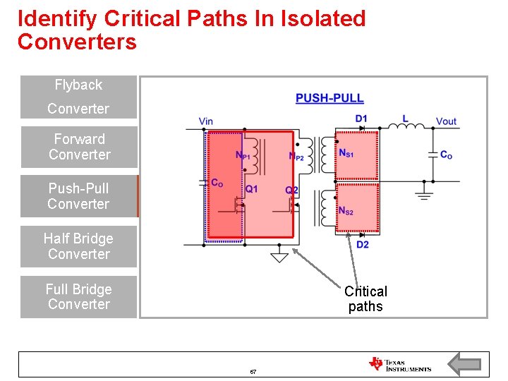
Identify Critical Paths In Isolated Converters Flyback Converter Forward Converter Push-Pull Converter Half Bridge Converter Critical paths Full Bridge Converter 66
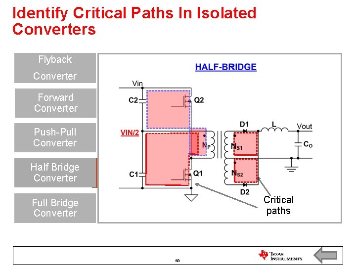
Identify Critical Paths In Isolated Converters Flyback Converter Forward Converter Push-Pull Converter Half Bridge Converter Full Bridge Converter Critical paths 67
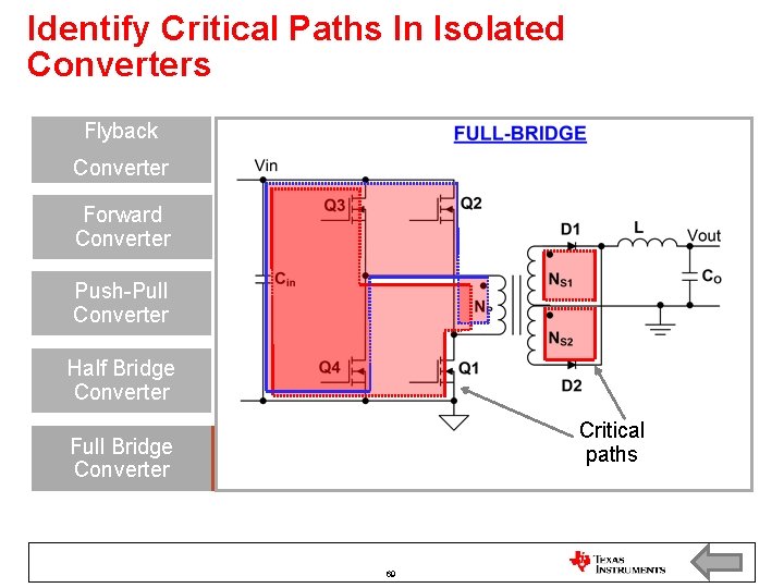
Identify Critical Paths In Isolated Converters Flyback Converter Forward Converter Push-Pull Converter Half Bridge Converter Critical paths Full Bridge Converter 68
Identify Critical Paths In Isolated Converters Flyback Converter Forward Converter Push-Pull Converter Half Bridge Converter Critical paths Full Bridge Converter 69
Isolated and High Power Density Board • The good practices and generic rules covered previously all apply to the isolated power board layout. • There are some additional considerations for isolated and high power density power boards: – Spacing requirement to sustain the potential difference between adjacent traces; – PC Board copper layer thickness and trace widths; – PC Board heatsink; – Isolation boundary. 70
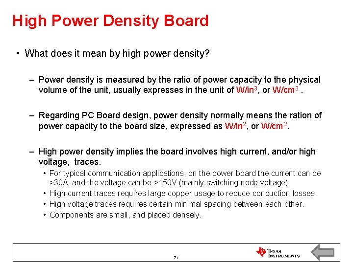
High Power Density Board • What does it mean by high power density? – Power density is measured by the ratio of power capacity to the physical volume of the unit, usually expresses in the unit of W/in 3, or W/cm 3. – Regarding PC Board design, power density normally means the ration of power capacity to the board size, expressed as W/in 2, or W/cm 2. – High power density implies the board involves high current, and/or high voltage, traces. • For typical communication applications, on the power board the current can be >30 A, and the voltage can be >150 V (mainly switching node voltage). • High current traces requires large copper usage to reduce conduction losses • High voltage traces requires certain minimal spacing between each other. • Components are small, and placed densely. 71
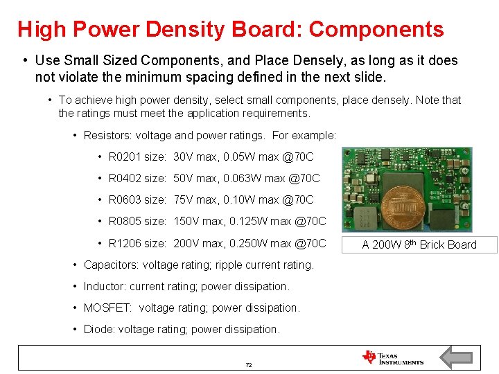
High Power Density Board: Components • Use Small Sized Components, and Place Densely, as long as it does not violate the minimum spacing defined in the next slide. • To achieve high power density, select small components, place densely. Note that the ratings must meet the application requirements. • Resistors: voltage and power ratings. For example: • R 0201 size: 30 V max, 0. 05 W max @70 C • R 0402 size: 50 V max, 0. 063 W max @70 C • R 0603 size: 75 V max, 0. 10 W max @70 C • R 0805 size: 150 V max, 0. 125 W max @70 C • R 1206 size: 200 V max, 0. 250 W max @70 C • Capacitors: voltage rating; ripple current rating. • Inductor: current rating; power dissipation. • MOSFET: voltage rating; power dissipation. • Diode: voltage rating; power dissipation. 72 A 200 W 8 th Brick Board
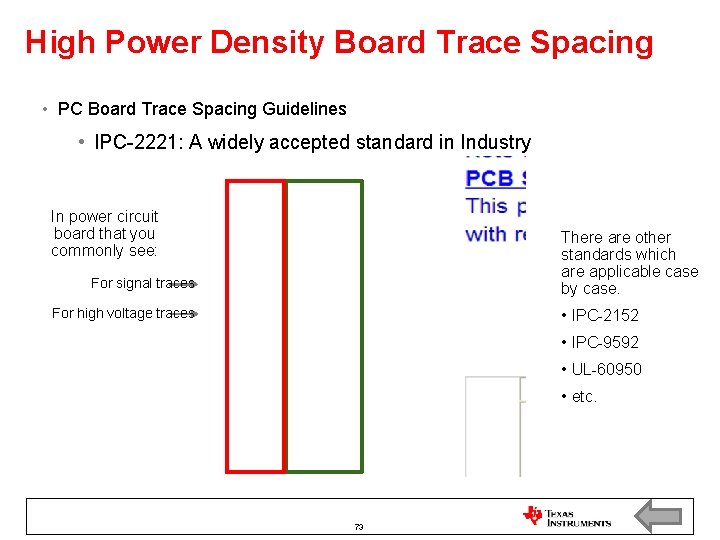
High Power Density Board Trace Spacing • PC Board Trace Spacing Guidelines • IPC-2221: A widely accepted standard in Industry In power circuit board that you commonly see: There are other standards which are applicable case by case. For signal traces For high voltage traces • IPC-2152 • IPC-9592 • UL-60950 • etc. 73
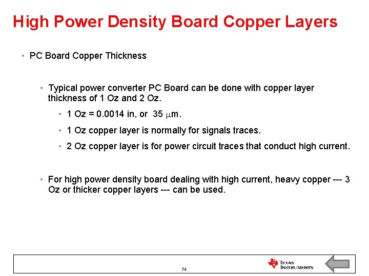
High Power Density Board Copper Layers • PC Board Copper Thickness • Typical power converter PC Board can be done with copper layer thickness of 1 Oz and 2 Oz. • 1 Oz = 0. 0014 in, or 35 m. • 1 Oz copper layer is normally for signals traces. • 2 Oz copper layer is for power circuit traces that conduct high current. • For high power density board dealing with high current, heavy copper --- 3 Oz or thicker copper layers --- can be used. 74
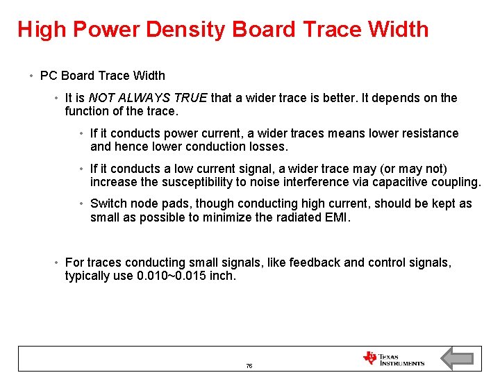
High Power Density Board Trace Width • PC Board Trace Width • It is NOT ALWAYS TRUE that a wider trace is better. It depends on the function of the trace. • If it conducts power current, a wider traces means lower resistance and hence lower conduction losses. • If it conducts a low current signal, a wider trace may (or may not) increase the susceptibility to noise interference via capacitive coupling. • Switch node pads, though conducting high current, should be kept as small as possible to minimize the radiated EMI. • For traces conducting small signals, like feedback and control signals, typically use 0. 010~0. 015 inch. 75
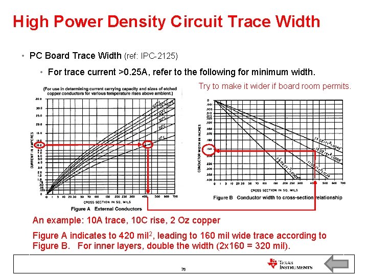
High Power Density Circuit Trace Width • PC Board Trace Width (ref: IPC-2125) • For trace current >0. 25 A, refer to the following for minimum width. Try to make it wider if board room permits. An example: 10 A trace, 10 C rise, 2 Oz copper Figure A indicates to 420 mil 2, leading to 160 mil wide trace according to Figure B. For inner layers, double the width (2 x 160 = 320 mil). 76
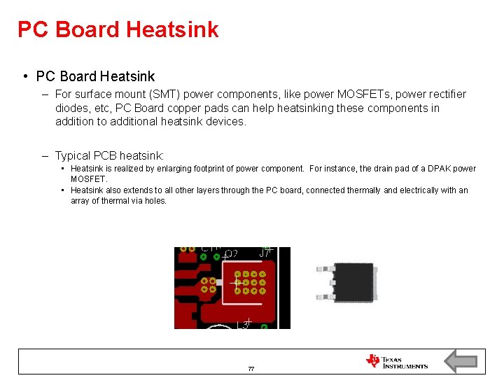
PC Board Heatsink • PC Board Heatsink – For surface mount (SMT) power components, like power MOSFETs, power rectifier diodes, etc, PC Board copper pads can help heatsinking these components in addition to additional heatsink devices. – Typical PCB heatsink: • Heatsink is realized by enlarging footprint of power component. For instance, the drain pad of a DPAK power MOSFET. • Heatsink also extends to all other layers through the PC board, connected thermally and electrically with an array of thermal via holes. 77
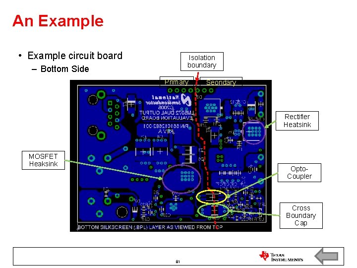
Isolation Boundary • Isolation boundary – Depending on application, the requirement of isolation strength is different. • For telecom, it is usually 1. 5 k. Vac rms, or 2. 2 k. V dc. • For medical, it is 2. 5 k. Vac rms up to 5 k. Vac rms. • Some applications may require 10. 1 k. Vdc. – Isolation boundary needs to be clear of conductors, or clear of copper traces. The clearance should confirm the spacing per applicable safety regulations and standards. – In power supply, there are four types of devices that are usually placed across the isolation boundary. • • Power transformers fulfilling isolated power transfer Opto-couplers, or solid state isolators Pulse transformers for isolated gate drive A common mode capacitor (always reserve a position on PCB, even if not intended to use initially). 78
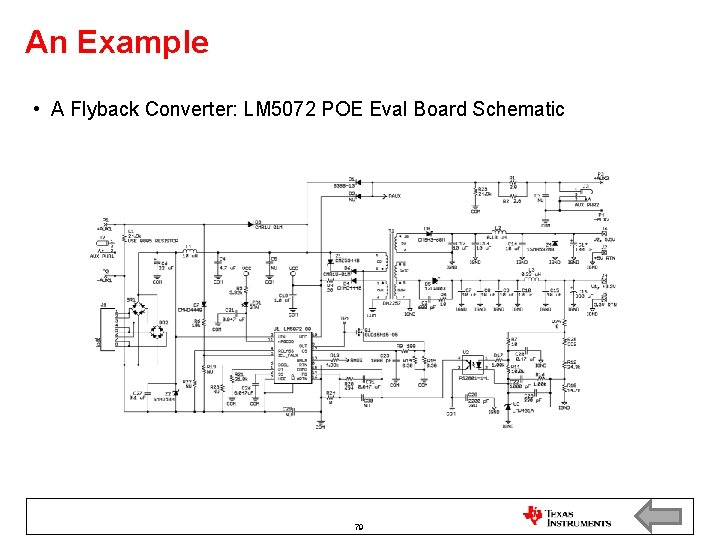
An Example • A Flyback Converter: LM 5072 POE Eval Board Schematic 79
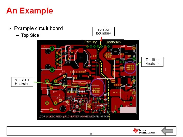
An Example • Example circuit board Isolation boundary – Top Side Primary Seondary Rectifier Heatsink MOSFET Heaksink 80
An Example • Example circuit board Isolation boundary – Bottom Side Primary Seondary Rectifier Heatsink MOSFET Heaksink Opto. Coupler Cross Boundary Cap 81
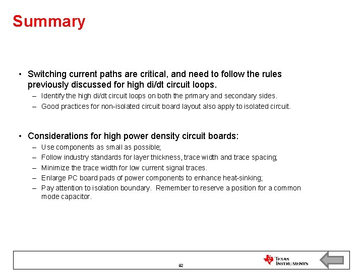
Summary • Switching current paths are critical, and need to follow the rules previously discussed for high di/dt circuit loops. – Identify the high di/dt circuit loops on both the primary and secondary sides. – Good practices for non-isolated circuit board layout also apply to isolated circuit. • Considerations for high power density circuit boards: – – – Use components as small as possible; Follow industry standards for layer thickness, trace width and trace spacing; Minimize the trace width for low current signal traces. Enlarge PC board pads of power components to enhance heat-sinking; Pay attention to isolation boundary. Remember to reserve a position for a common mode capacitor. 82
Thank You 83
Appendix A) Snubbers David Baba Power Design Group 84
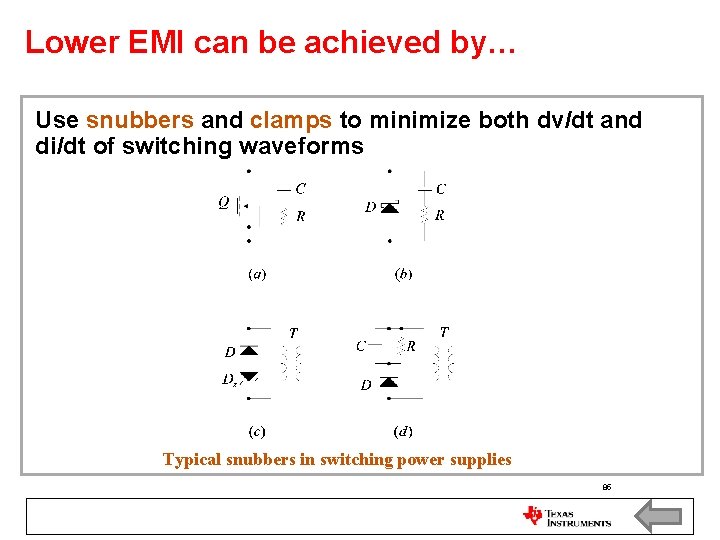
Lower EMI can be achieved by… Use snubbers and clamps to minimize both dv/dt and di/dt of switching waveforms Typical snubbers in switching power supplies 85
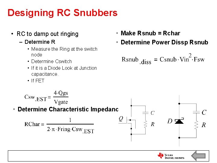
Designing RC Snubbers • RC to damp out ringing – Determine R • Make Rsnub = Rchar • Determine Power Dissp Rsnub • Measure the Ring at the switch node • Determine Cswitch • If it is a Diode Look at Junction capacitance. • If FET • Determine Characteristic Impedance
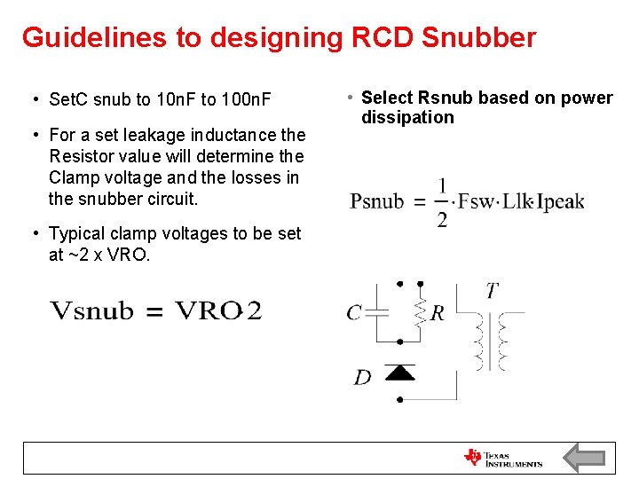
Guidelines to designing RCD Snubber • Set. C snub to 10 n. F to 100 n. F • For a set leakage inductance the Resistor value will determine the Clamp voltage and the losses in the snubber circuit. • Typical clamp voltages to be set at ~2 x VRO. • Select Rsnub based on power dissipation
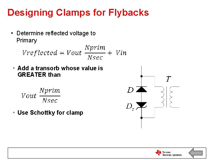
Designing Clamps for Flybacks • Determine reflected voltage to Primary • Add a transorb whose value is GREATER than • Use Schottky for clamp
Appendix B) Component Selection David Baba Power Design Group 89
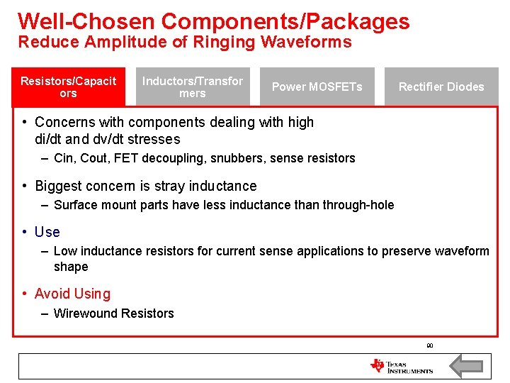
Well-Chosen Components/Packages Reduce Amplitude of Ringing Waveforms Resistors/Capacit ors Inductors/Transfor mers Power MOSFETs Rectifier Diodes • Concerns with components dealing with high di/dt and dv/dt stresses – Cin, Cout, FET decoupling, snubbers, sense resistors • Biggest concern is stray inductance – Surface mount parts have less inductance than through-hole • Use – Low inductance resistors for current sense applications to preserve waveform shape • Avoid Using – Wirewound Resistors 90
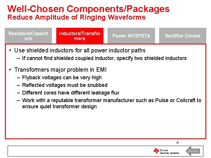
Well-Chosen Components/Packages Reduce Amplitude of Ringing Waveforms Resistors/Capacit ors Inductors/Transfor mers Power MOSFETs Rectifier Diodes • Use shielded inductors for all power inductor paths – If cannot find shielded coupled inductor, specify two shielded inductors • Transformers major problem in EMI – – Flyback voltages can be very high Reflected voltages must be snubbed Different cores have different leakage flux Work with a reputable transformer manufacturer such as Pulse or Coilcraft to ensure quiet transformer design 91
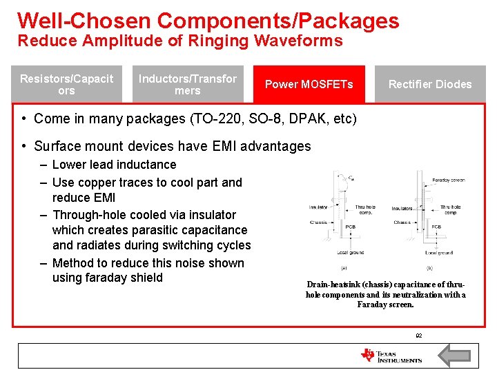
Well-Chosen Components/Packages Reduce Amplitude of Ringing Waveforms Resistors/Capacit ors Inductors/Transfor mers Power MOSFETs Rectifier Diodes • Come in many packages (TO-220, SO-8, DPAK, etc) • Surface mount devices have EMI advantages – Lower lead inductance – Use copper traces to cool part and reduce EMI – Through-hole cooled via insulator which creates parasitic capacitance and radiates during switching cycles – Method to reduce this noise shown using faraday shield Drain-heatsink (chassis) capacitance of thruhole components and its neutralization with a Faraday screen. 92
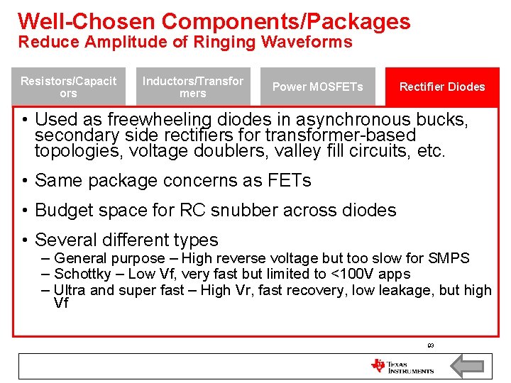
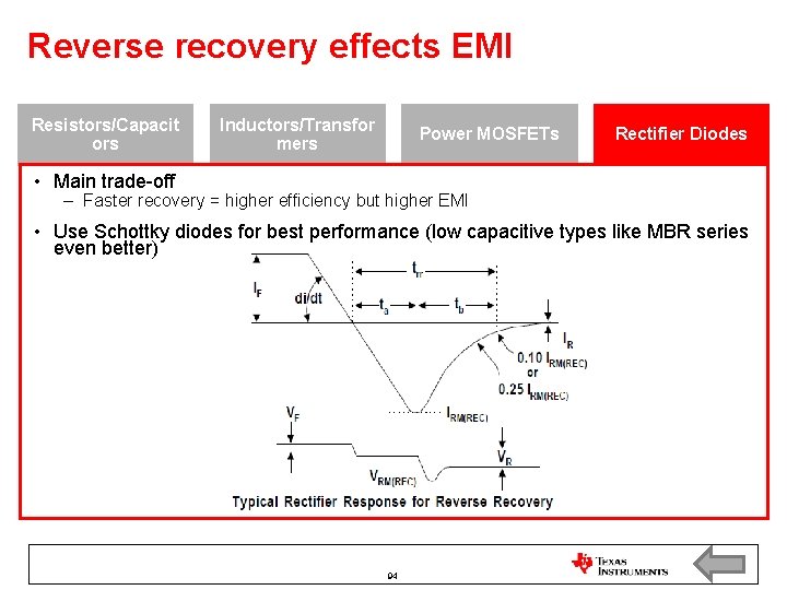
Well-Chosen Components/Packages Reduce Amplitude of Ringing Waveforms Resistors/Capacit ors Inductors/Transfor mers Power MOSFETs Rectifier Diodes • Used as freewheeling diodes in asynchronous bucks, secondary side rectifiers for transformer-based topologies, voltage doublers, valley fill circuits, etc. • Same package concerns as FETs • Budget space for RC snubber across diodes • Several different types – General purpose – High reverse voltage but too slow for SMPS – Schottky – Low Vf, very fast but limited to <100 V apps – Ultra and super fast – High Vr, fast recovery, low leakage, but high Vf 93
Reverse recovery effects EMI Resistors/Capacit ors Inductors/Transfor mers Power MOSFETs Rectifier Diodes • Main trade-off – Faster recovery = higher efficiency but higher EMI • Use Schottky diodes for best performance (low capacitive types like MBR series even better) 94
Thank You Questions? 95