Lecture 1213 SWITCHINGMODE POWER SUPPLIES 1 SwitchingMode Power

- Slides: 63

Lecture # 12&13 SWITCHING-MODE POWER SUPPLIES 1

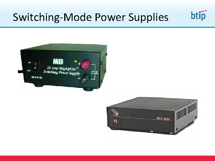
Switching-Mode Power Supplies 2

Introduction to Switching Regulators Objective of topic is to answer the following questions: 1. 2. 3. 4. 5. 6. 7. 8. What is a switching power supply? What types of switchers are available? Why is a switcher needed? How does a switcher operate in general? How does a buck converter operate? How does a boost converter operate? How does a buck-boost converter operate? How many design topologies of a switching power supplies? 3

Introduction to Switching Regulators Intended Audience: • Electrical engineers with limited power supply background • A simple, functional understanding of inductors and capacitors is assumed • A simple, functional understanding of transistors is assumed Expected Time: • Approximately 120 minutes 4

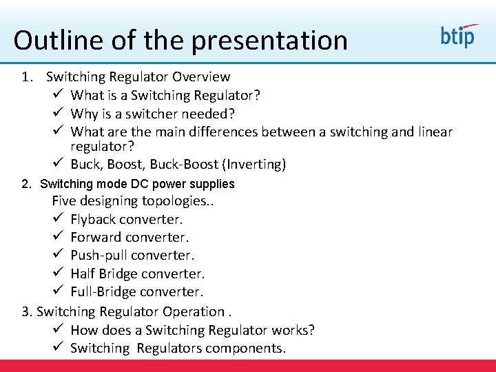
Outline of the presentation 1. Switching Regulator Overview ü What is a Switching Regulator? ü Why is a switcher needed? ü What are the main differences between a switching and linear regulator? ü Buck, Boost, Buck-Boost (Inverting) 2. Switching mode DC power supplies Five designing topologies. . ü Flyback converter. ü Forward converter. ü Push-pull converter. ü Half Bridge converter. ü Full-Bridge converter. 3. Switching Regulator Operation. ü How does a Switching Regulator works? ü Switching Regulators components. 5

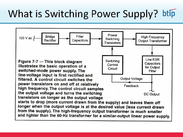
What is Switching Power Supply? 6

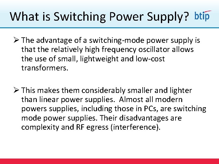
What is Switching Power Supply? Ø The advantage of a switching-mode power supply is that the relatively high frequency oscillator allows the use of small, lightweight and low-cost transformers. Ø This makes them considerably smaller and lighter than linear power supplies. Almost all modern powers supplies, including those in PCs, are switching mode power supplies. Their disadvantages are complexity and RF egress (interference). 7

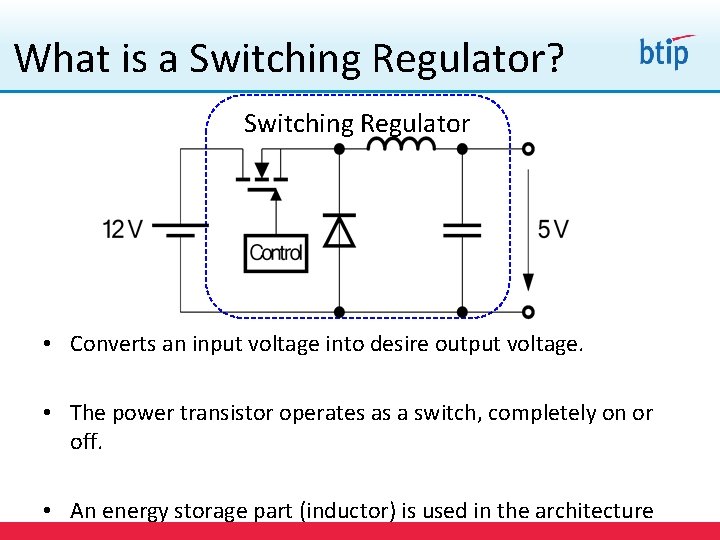
What is a Switching Regulator? Switching Regulator • Converts an input voltage into desire output voltage. • The power transistor operates as a switch, completely on or off. • An energy storage part (inductor) is used in the architecture 8

Choosing Between Linear and Switching Regulators • When possible, most designers would prefer to use a linear voltage regulator rather than a switching voltage regulator • Linear regulators are usually lower in price • Linear regulators are usually simpler to implement • Linear regulators do not have associated noise/ripple problems apparent in switching regulators 9

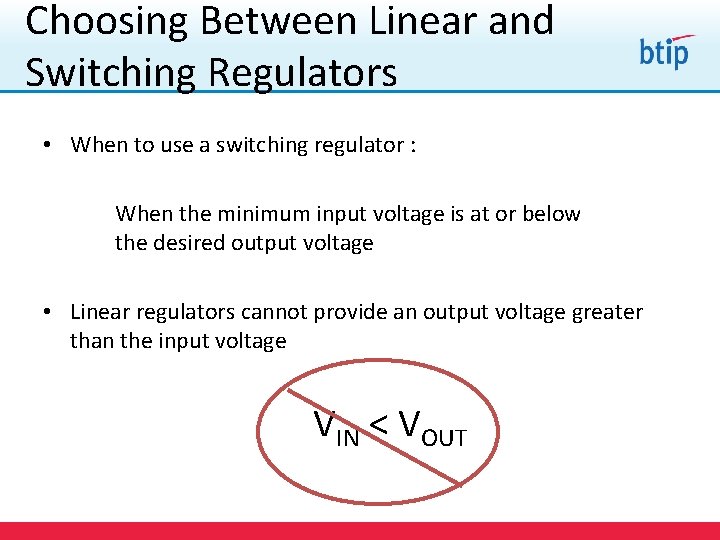
Choosing Between Linear and Switching Regulators • When to use a switching regulator : When the minimum input voltage is at or below the desired output voltage • Linear regulators cannot provide an output voltage greater than the input voltage V < VOUT IN 10

Choosing Between Linear and Switching Regulators • When to use a switching regulator: • The efficiency of a linear regulator cannot maintain the junction temperature below the specified maximum • The maximum junction temperature is usually 150 C • The efficiency of linear regulators often prohibit their use in high voltage, high current applications 11

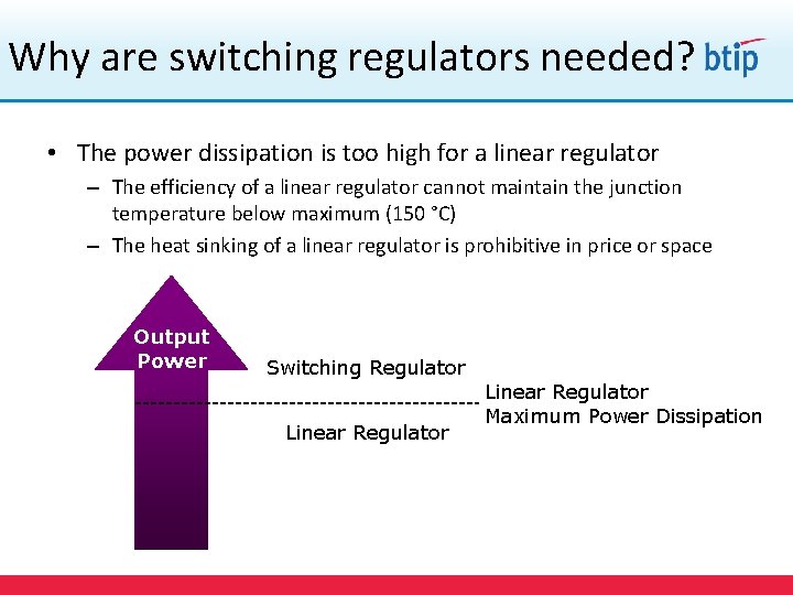
Why are switching regulators needed? • The power dissipation is too high for a linear regulator – The efficiency of a linear regulator cannot maintain the junction temperature below maximum (150 °C) – The heat sinking of a linear regulator is prohibitive in price or space Output Power Switching Regulator Linear Regulator Maximum Power Dissipation 12

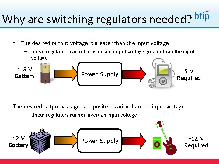
Why are switching regulators needed? • The desired output voltage is greater than the input voltage – Linear regulators cannot provide an output voltage greater than the input voltage 1. 5 V Battery Power Supply 5 V Required The desired output voltage is opposite polarity than the input voltage – Linear regulators cannot invert an input voltage 12 V Battery Power Supply -12 V Required 13

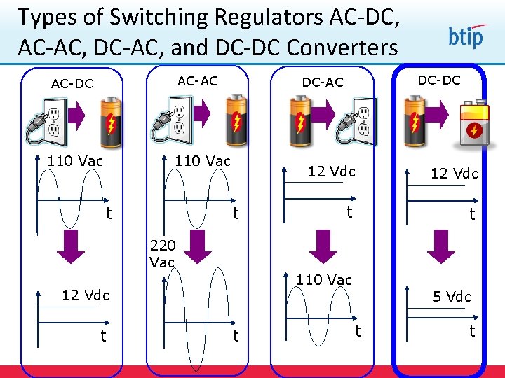
Types of Switching Regulators AC-DC, AC-AC, DC-AC, and DC-DC Converters AC-AC AC-DC 110 Vac t DC-DC DC-AC t 12 Vdc t t 220 Vac 110 Vac 12 Vdc t 5 Vdc t t t 14

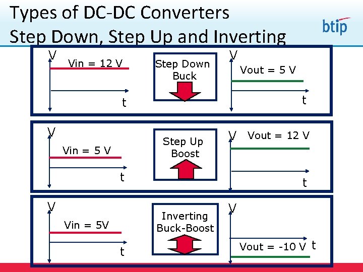
Types of DC-DC Converters Step Down, Step Up and Inverting V Vin = 12 V Step Down Buck V Vout = 5 V t t V Step Up Boost Vin = 5 V V Vout = 12 V t Inverting Buck-Boost Vin = 5 V t V Vout = -10 V t 15

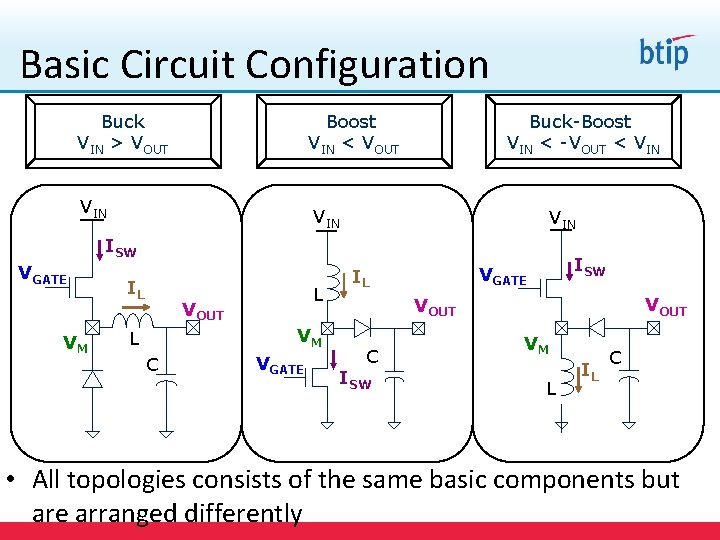
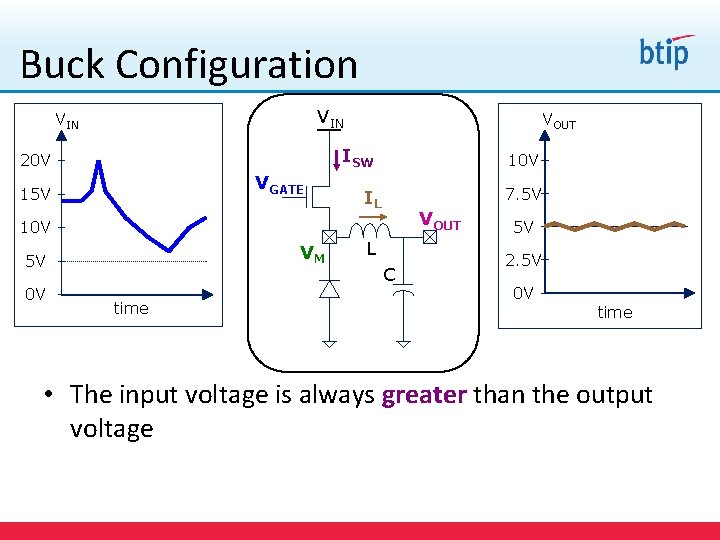
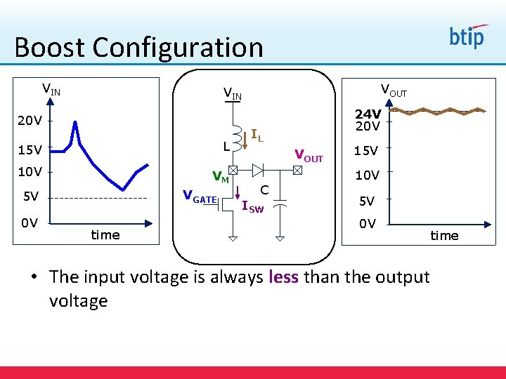
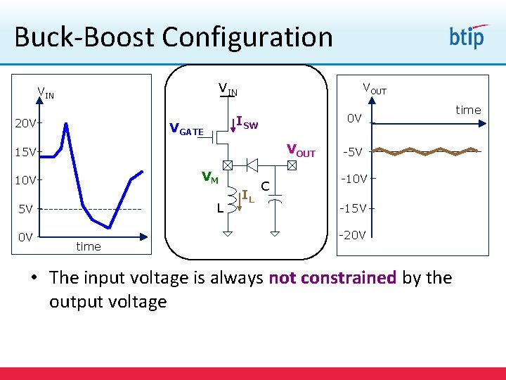
Basic Circuit Configuration Buck VIN > VOUT Boost VIN < VOUT VIN Buck-Boost VIN < -VOUT < VIN VIN ISW VGATE VM IL L VOUT VM L C VGATE ISW VGATE IL VOUT C ISW VM L IL C • All topologies consists of the same basic components but 16 are arranged differently

Buck Configuration VIN VOUT ISW 20 V VGATE 15 V 10 V 7. 5 V IL VOUT 10 V VM 5 V 0 V time L C 5 V 2. 5 V 0 V time • The input voltage is always greater than the output voltage 17

Boost Configuration VIN 20 V 15 V L 10 V VM VGATE 5 V 0 V VOUT VIN time 24 V 20 V IL VOUT C ISW 15 V 10 V 5 V 0 V time • The input voltage is always less than the output voltage 18

Buck-Boost Configuration VIN 20 V VOUT 0 V ISW VGATE VOUT 15 V VM 10 V L 5 V 0 V time IL C time -5 V -10 V -15 V -20 V • The input voltage is always not constrained by the output voltage 19

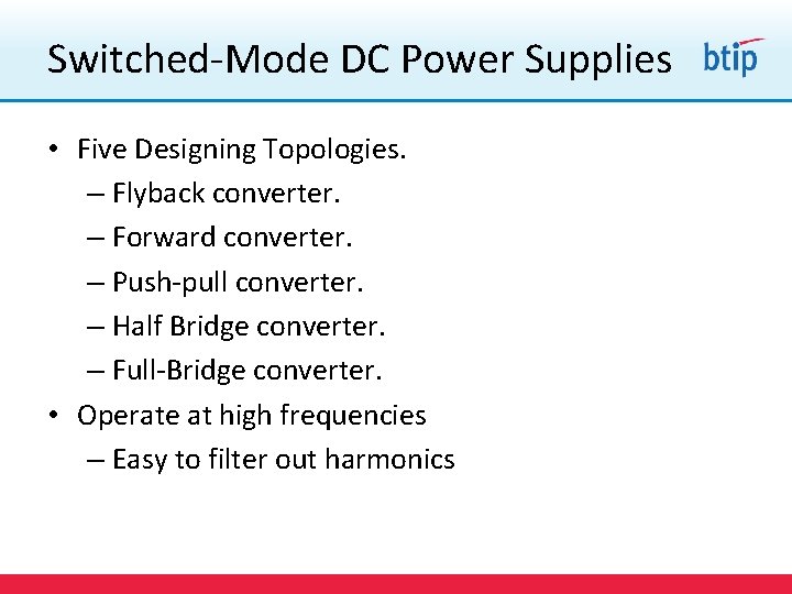
Switched-Mode DC Power Supplies • Five Designing Topologies. – Flyback converter. – Forward converter. – Push-pull converter. – Half Bridge converter. – Full-Bridge converter. • Operate at high frequencies – Easy to filter out harmonics 20

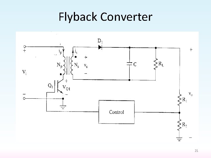
Flyback Converter 21

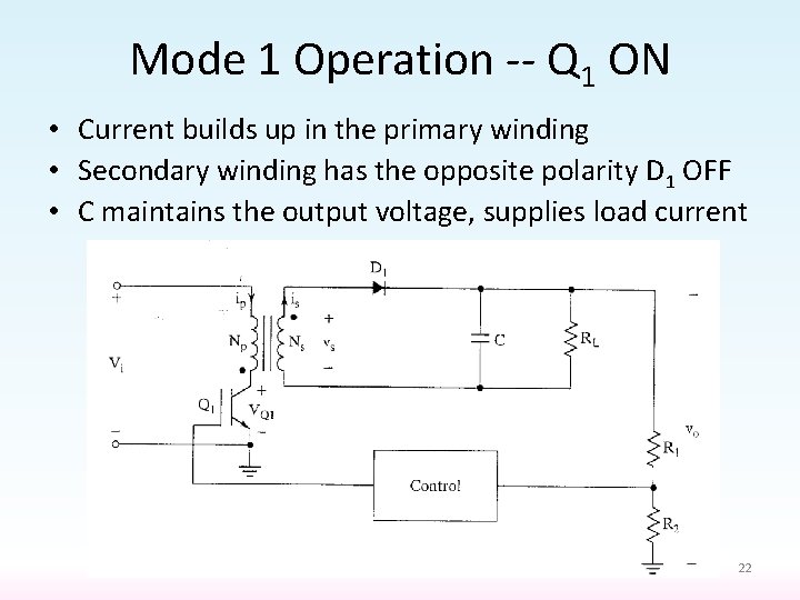
Mode 1 Operation -- Q 1 ON • Current builds up in the primary winding • Secondary winding has the opposite polarity D 1 OFF • C maintains the output voltage, supplies load current 22

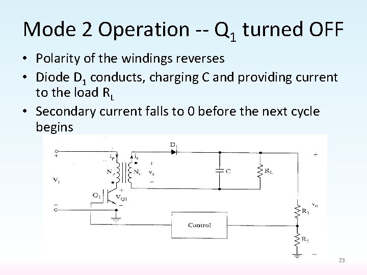
Mode 2 Operation -- Q 1 turned OFF • Polarity of the windings reverses • Diode D 1 conducts, charging C and providing current to the load RL • Secondary current falls to 0 before the next cycle begins 23

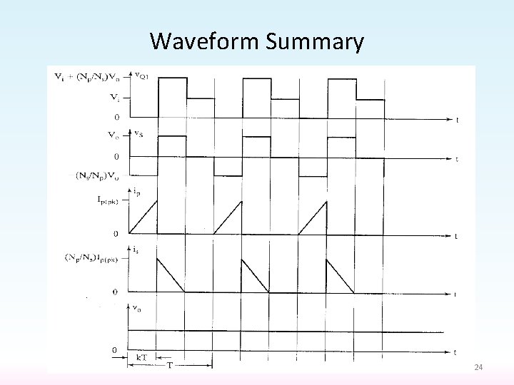
Waveform Summary 24

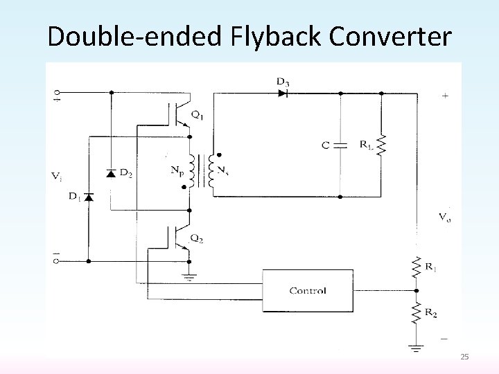
Double-ended Flyback Converter 25

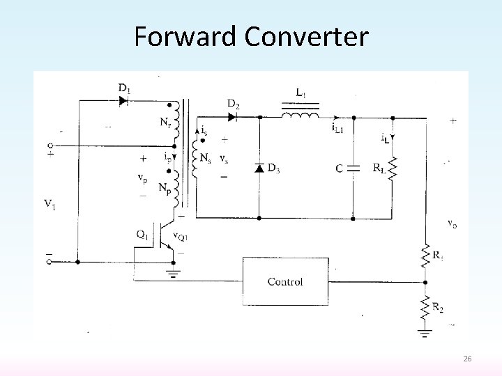
Forward Converter 26

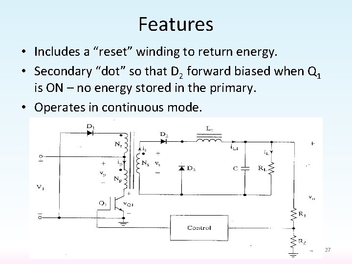
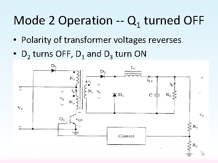
Features • Includes a “reset” winding to return energy. • Secondary “dot” so that D 2 forward biased when Q 1 is ON – no energy stored in the primary. • Operates in continuous mode. 27

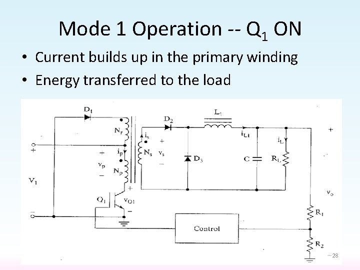
Mode 1 Operation -- Q 1 ON • Current builds up in the primary winding • Energy transferred to the load 28

Mode 2 Operation -- Q 1 turned OFF • Polarity of transformer voltages reverses • D 2 turns OFF, D 1 and D 3 turn ON 29

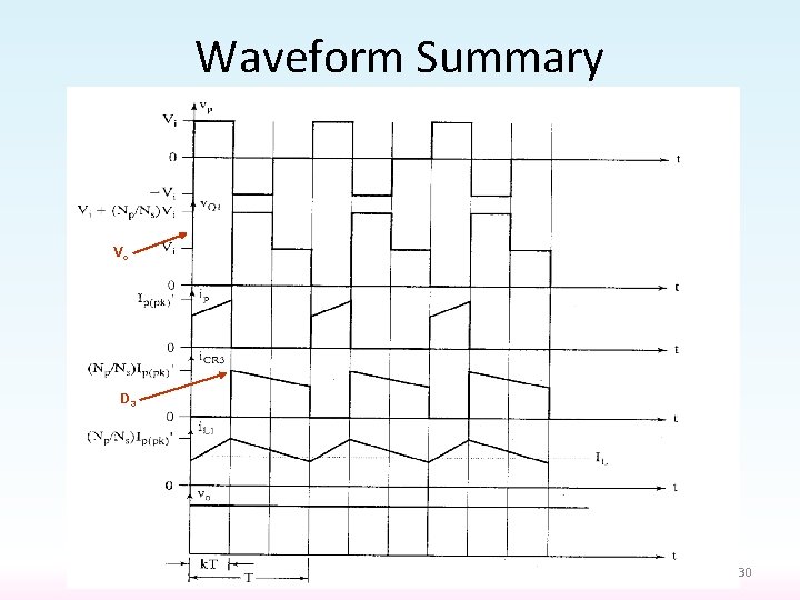
Waveform Summary Vo D 3 30

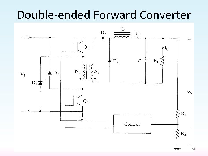
Double-ended Forward Converter 31

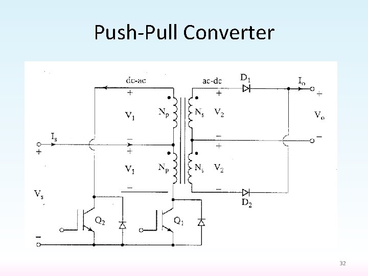
Push-Pull Converter 32

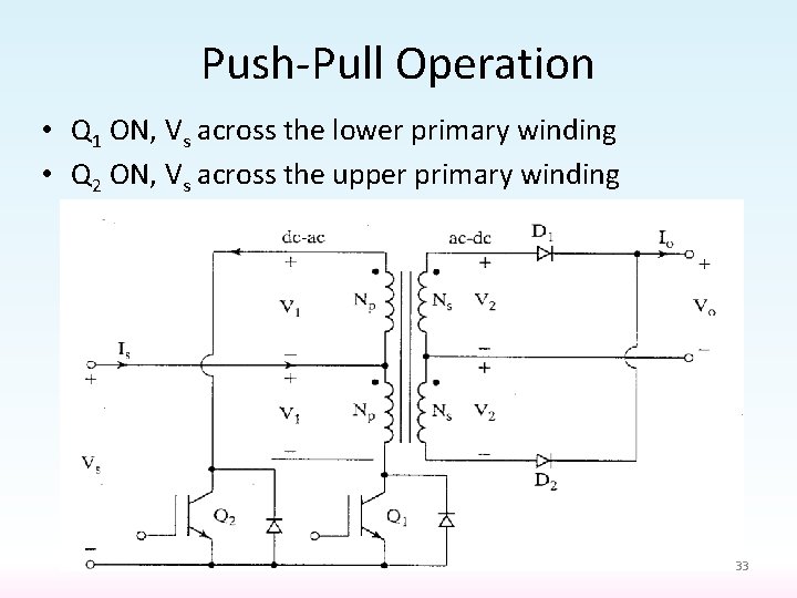
Push-Pull Operation • Q 1 ON, Vs across the lower primary winding • Q 2 ON, Vs across the upper primary winding 33

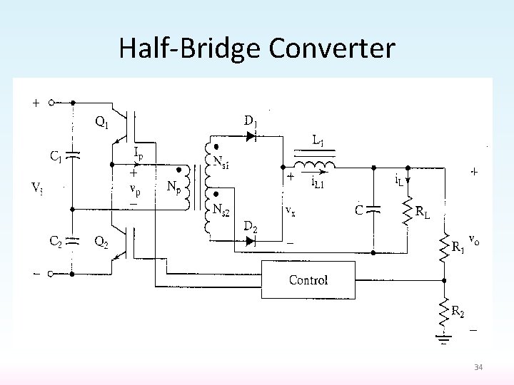
Half-Bridge Converter 34

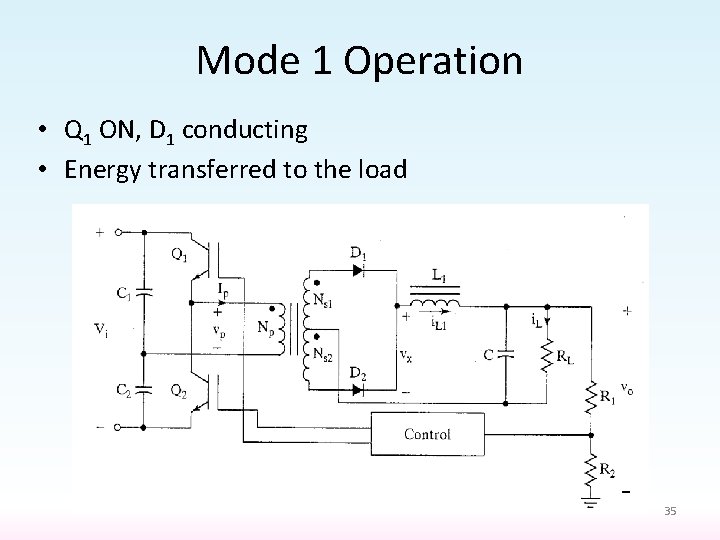
Mode 1 Operation • Q 1 ON, D 1 conducting • Energy transferred to the load 35

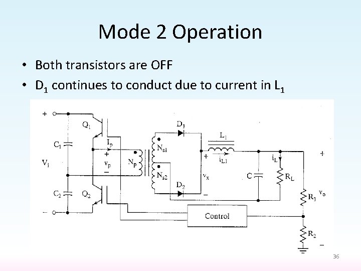
Mode 2 Operation • Both transistors are OFF • D 1 continues to conduct due to current in L 1 36

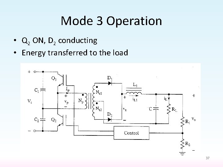
Mode 3 Operation • Q 2 ON, D 2 conducting • Energy transferred to the load 37

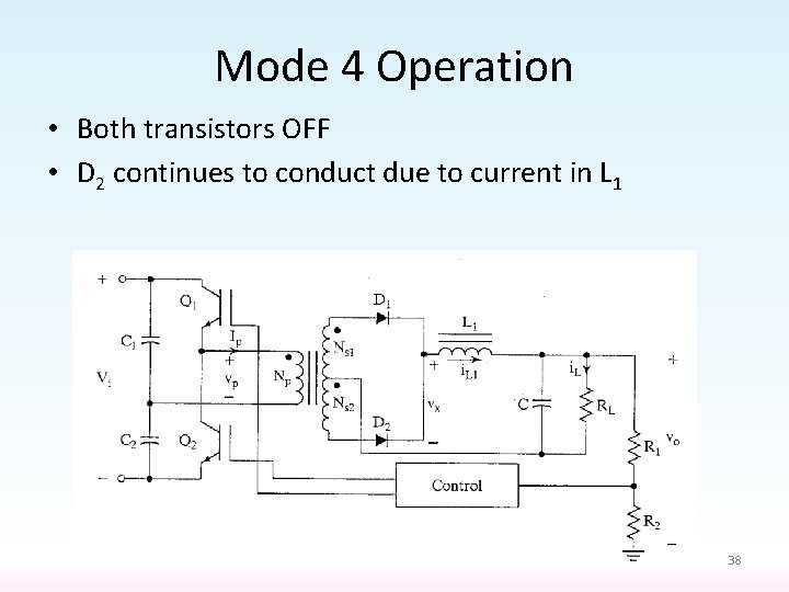
Mode 4 Operation • Both transistors OFF • D 2 continues to conduct due to current in L 1 38

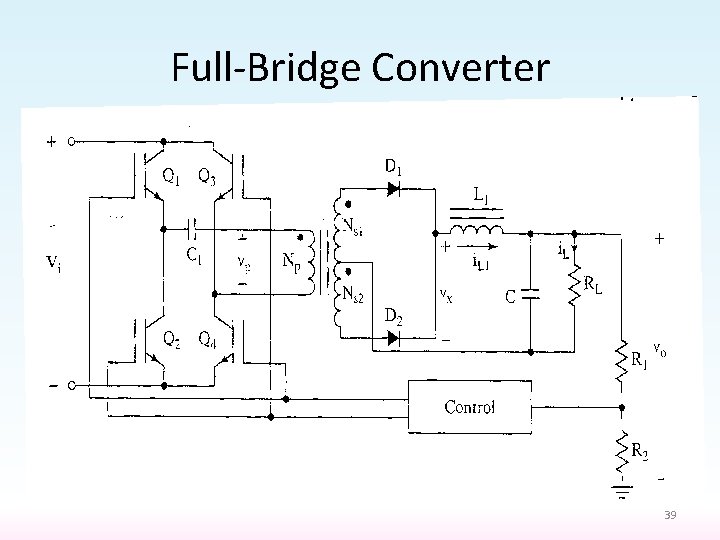
Full-Bridge Converter 39

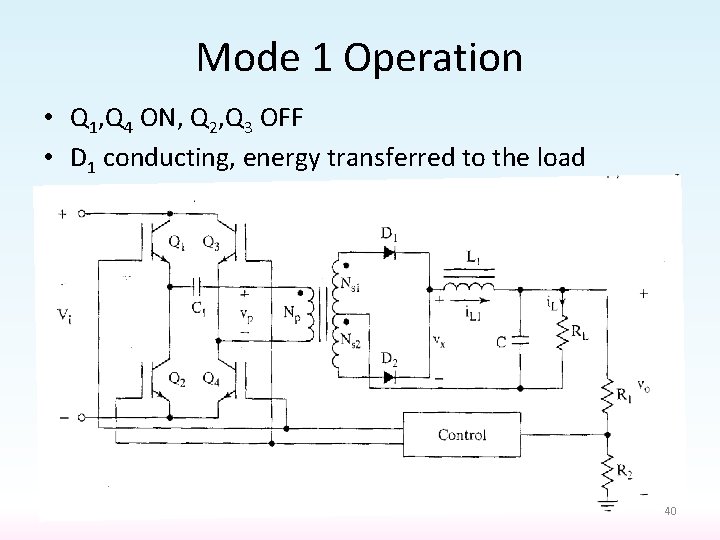
Mode 1 Operation • Q 1, Q 4 ON, Q 2, Q 3 OFF • D 1 conducting, energy transferred to the load 40

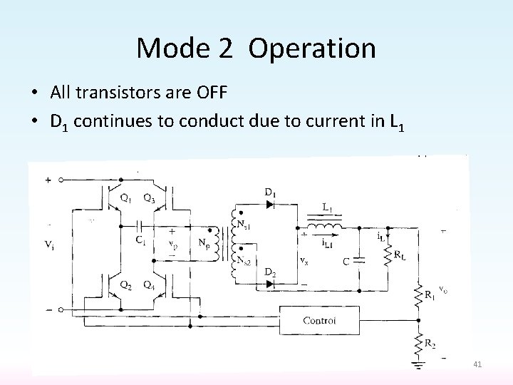
Mode 2 Operation • All transistors are OFF • D 1 continues to conduct due to current in L 1 41

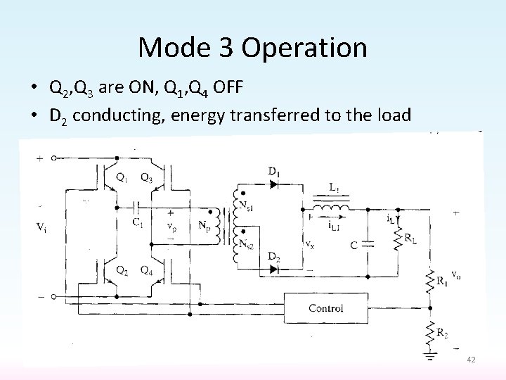
Mode 3 Operation • Q 2, Q 3 are ON, Q 1, Q 4 OFF • D 2 conducting, energy transferred to the load 42

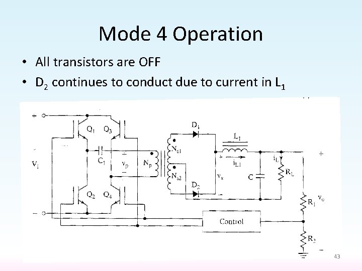
Mode 4 Operation • All transistors are OFF • D 2 continues to conduct due to current in L 1 43

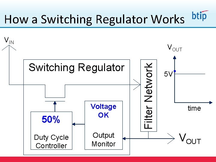
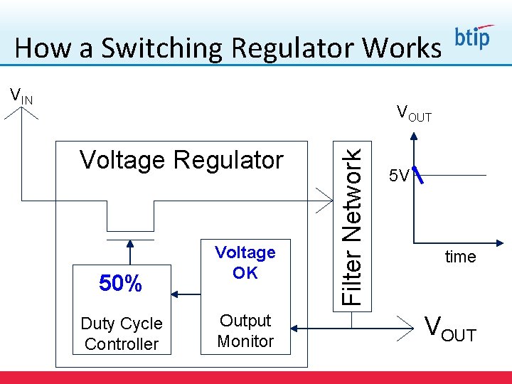
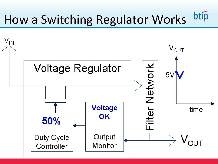
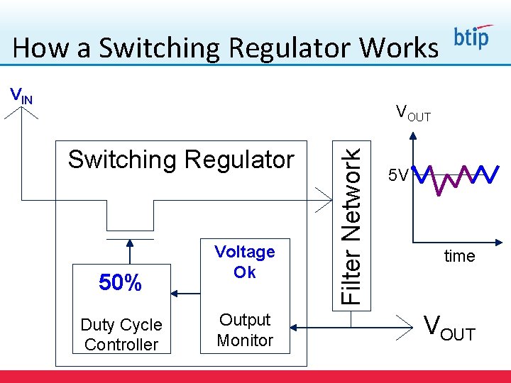
How a Switching Regulator Works VIN Switching Regulator 50% Duty Cycle Controller Voltage OK Output Monitor Filter Network VOUT 5 V time VOUT 44

How a Switching Regulator Works VIN Voltage Regulator 50% Duty Cycle Controller Voltage OK Output Monitor Filter Network VOUT 5 V time VOUT 45

How a Switching Regulator Works VIN Voltage Regulator 50% Duty Cycle Controller Voltage OK Output Monitor Filter Network VOUT 5 V time VOUT 46

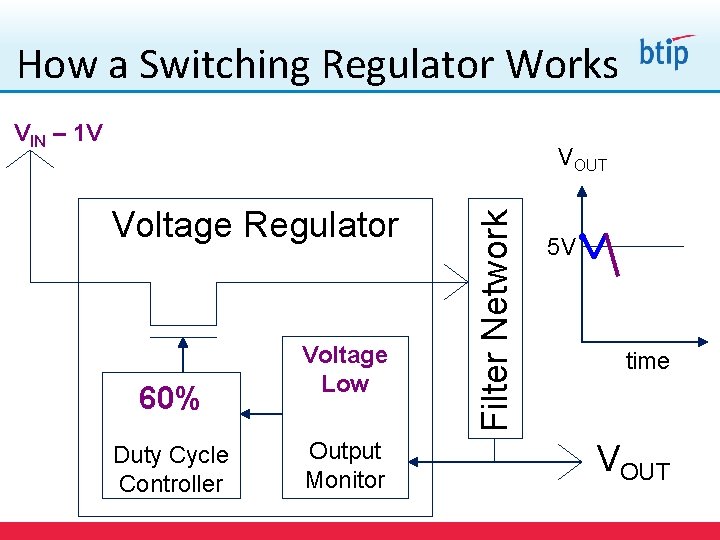
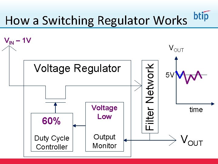
How a Switching Regulator Works VIN – 1 V Voltage Regulator 60% Duty Cycle Controller Voltage Low Output Monitor Filter Network VOUT 5 V time VOUT 47

How a Switching Regulator Works VIN – 1 V Voltage Regulator 60% Duty Cycle Controller Voltage Low Output Monitor Filter Network VOUT 5 V time VOUT 48

How a Switching Regulator Works VIN Switching Regulator 50% Duty Cycle Controller Voltage Ok Output Monitor Filter Network VOUT 5 V time VOUT 49

Switching Regulator Components 50

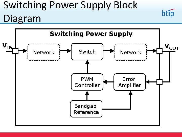
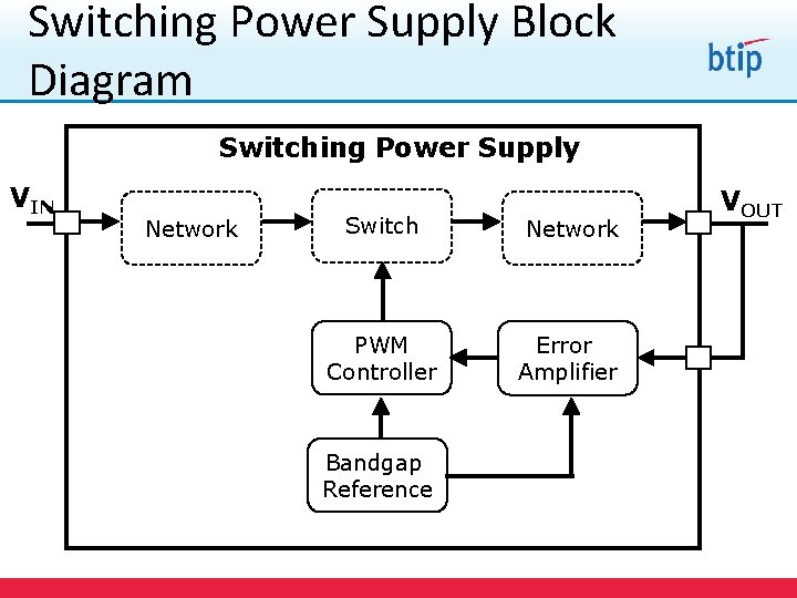
Switching Power Supply Block Diagram Switching Power Supply VIN Network Switch Network PWM Controller Error Amplifier VOUT Bandgap Reference 51

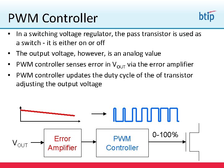
PWM Controller • In a switching voltage regulator, the pass transistor is used as a switch - it is either on or off • The output voltage, however, is an analog value • PWM controller senses error in VOUT via the error amplifier • PWM controller updates the duty cycle of the of transistor adjusting the output voltage VOUT Error Amplifier PWM Controller 0 -100% 52

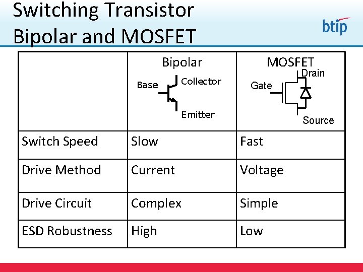
Switching Transistor Bipolar and MOSFET Bipolar Base Collector MOSFET Drain Gate Emitter Source Switch Speed Slow Fast Drive Method Current Voltage Drive Circuit Complex Simple ESD Robustness High Low 53

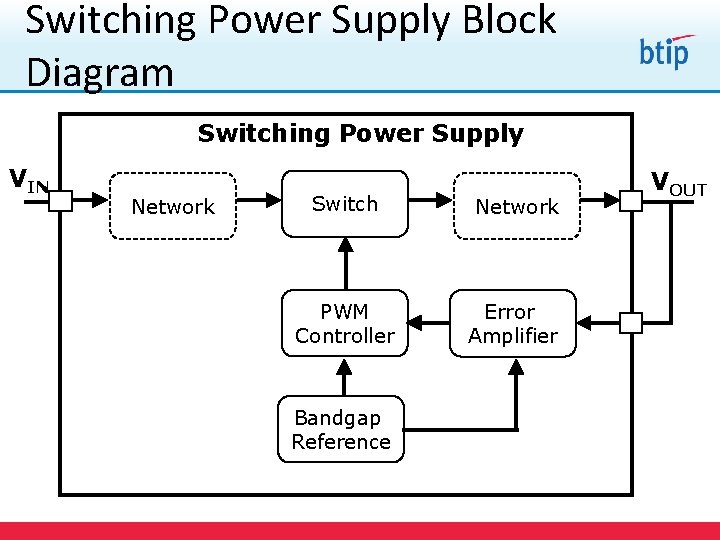
Switching Power Supply Block Diagram Switching Power Supply VIN Network Switch Network PWM Controller Error Amplifier VOUT Bandgap Reference 54

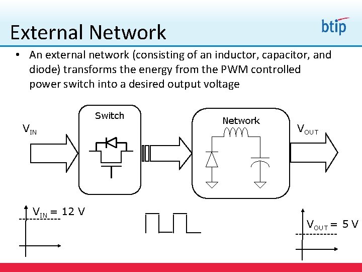
External Network • An external network (consisting of an inductor, capacitor, and diode) transforms the energy from the PWM controlled power switch into a desired output voltage Switch VIN = 12 V Network VOUT = 5 V 55

Switching Power Supply Block Diagram Switching Power Supply VIN Network Switch Network PWM Controller Error Amplifier VOUT Bandgap Reference 56

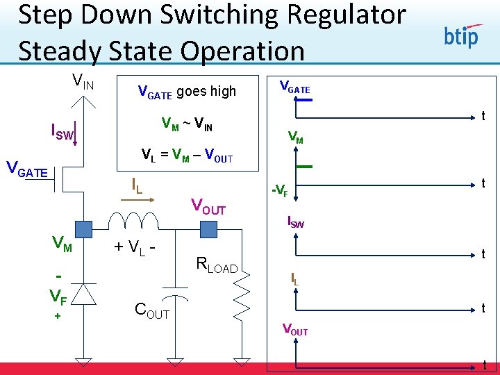
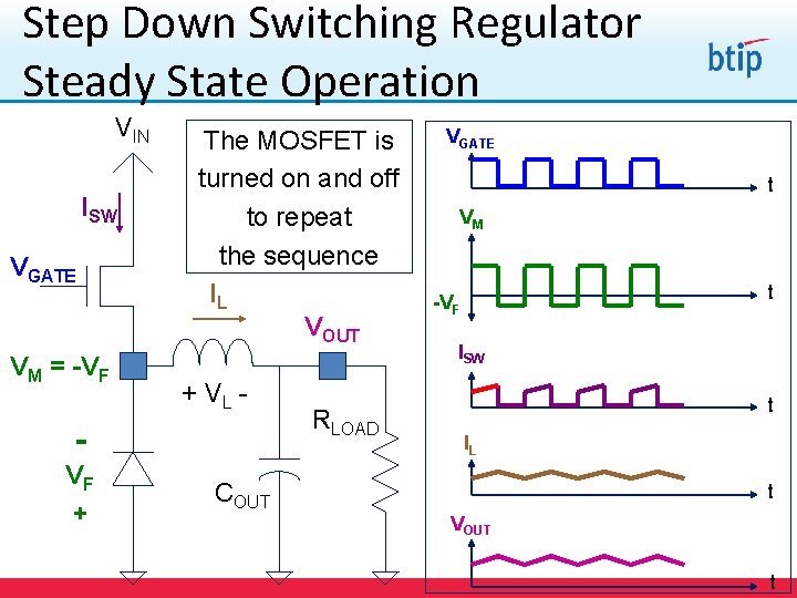
Step Down Switching Regulator Steady State Operation VIN VGATE goes high VM ~ VIN ISW VGATE t VM VL = VM – VOUT VGATE IL VM VF + + VL - VOUT RLOAD t -VF ISW t IL COUT t VOUT 57 t

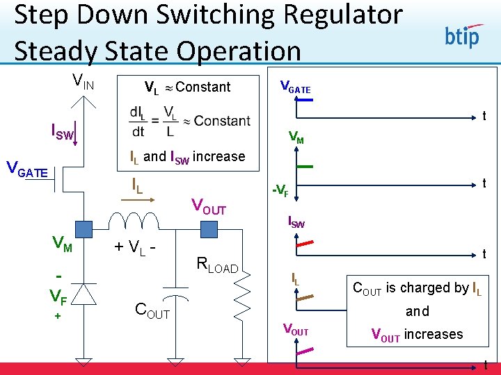
Step Down Switching Regulator Steady State Operation VIN VL Constant VGATE t ISW VM IL and ISW increase VGATE IL VM VF + + VL - VOUT RLOAD t -VF ISW t IL COUT is charged by IL t and VOUT increases 58 t

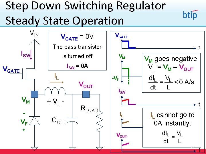
Step Down Switching Regulator Steady State Operation VIN ISW VGATE = 0 V VGATE The pass transistor is turned off t VM ISW = 0 A VGATE IL VM VF + + VL COUT VOUT RLOAD VM goes negative VL = VM – VOUT t -VF ISW t IL IL cannot go to 0 A instantly: t VOUT 59 t

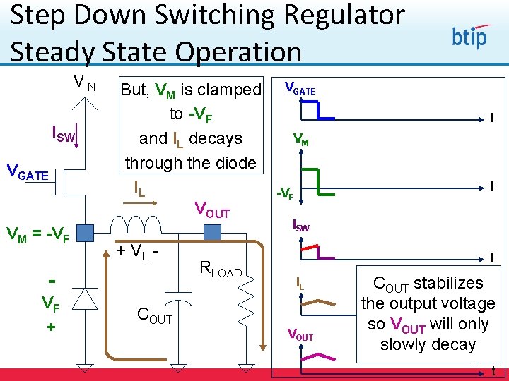
Step Down Switching Regulator Steady State Operation VIN ISW VGATE VM = -VF But, VM is clamped to -VF and IL decays through the diode IL VOUT + VL - VF + RLOAD VGATE t VM t -VF ISW t IL COUT VOUT COUT stabilizes the output voltaget so VOUT will only slowly decay 60 t

Step Down Switching Regulator Steady State Operation VIN ISW VGATE VM = -VF The MOSFET is turned on and off to repeat the sequence IL VOUT + VL - VF + RLOAD VGATE t VM t -VF ISW t IL COUT t VOUT 61 t

REFERENCES Ø For student study : Ø Read Chapter 21 discrete & integrated voltage regulators topics (21. 5) from the book introductory electronic devices and circuits by (Robert T. paynter)conventional flow version. Ø Wikipedia & world wide web. 62

THANK YOU! 63