High speed pipelined ADC Multiplexer for CALICE Why

- Slides: 13

High speed pipelined ADC + Multiplexer for CALICE

Why this high speed (25 MS/s) • Because pipeline is not power efficient below 10 MHz. • For a good FOM, the converter must be used at high frequency affordable by the process.

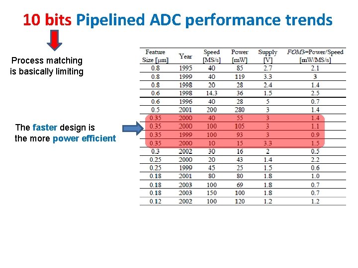
10 bits Pipelined ADC performance trends Process matching is basically limiting The faster design is the more power efficient

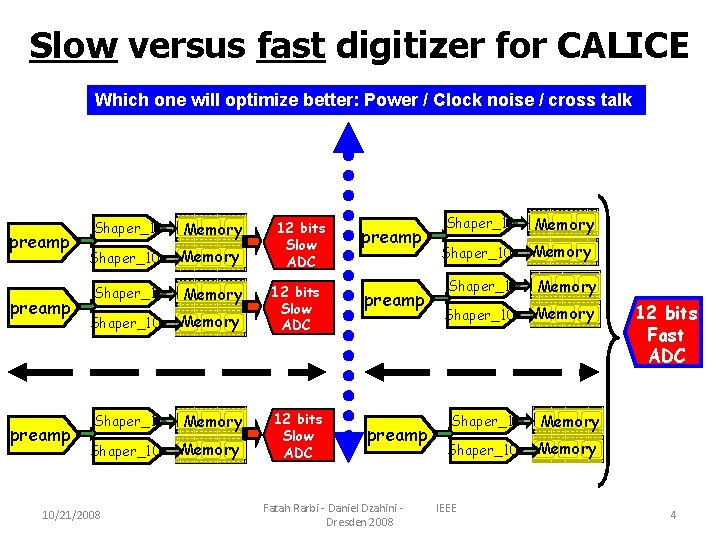
Slow versus fast digitizer for CALICE Which one will optimize better: Power / Clock noise / cross talk preamp Shaper_1 Memory Shaper_10 Memory 10/21/2008 12 bits Slow ADC preamp Fatah Rarbi - Daniel Dzahini Dresden 2008 Shaper_1 Memory Shaper_10 Memory IEEE 12 bits Fast ADC 4

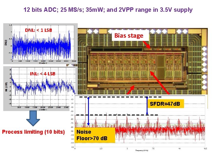
12 bits ADC; 25 MS/s; 35 m. W; and 2 VPP range in 3. 5 V supply DNL: < 1 LSB Bias stage INL: < 4 LSB Digital correction Process limiting (10 bits) Noise Floor>70 d. B 1. 5 bit stage SFDR=47 d. B

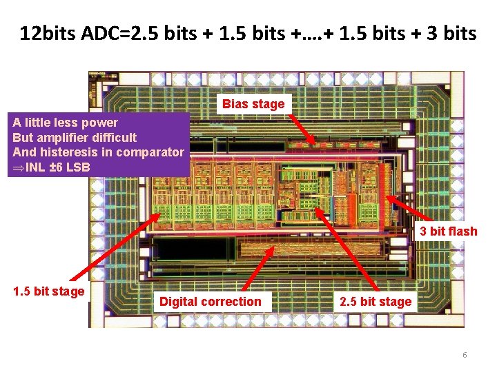
12 bits ADC=2. 5 bits + 1. 5 bits +…. + 1. 5 bits + 3 bits Bias stage A little less power But amplifier difficult And histeresis in comparator ÞINL ± 6 LSB 3 bit flash 1. 5 bit stage Digital correction 2. 5 bit stage 6

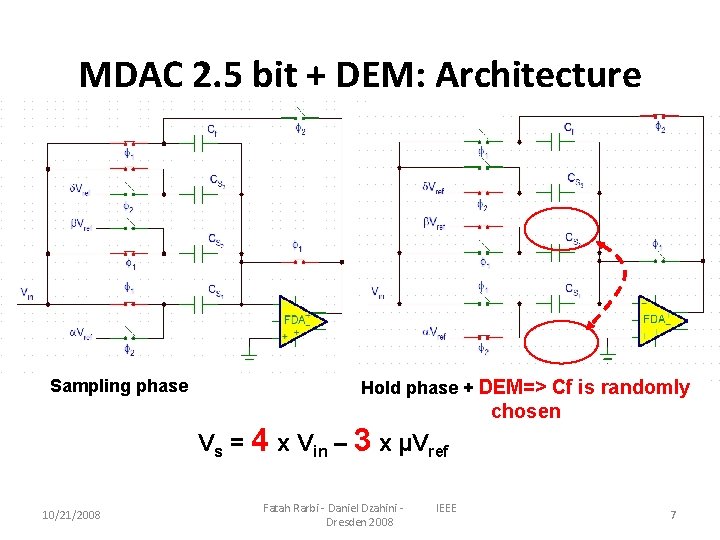
MDAC 2. 5 bit + DEM: Architecture Sampling phase Hold phase + DEM=> Cf is randomly Vs = 4 x Vin – 3 x µVref 10/21/2008 Fatah Rarbi - Daniel Dzahini Dresden 2008 IEEE chosen 7

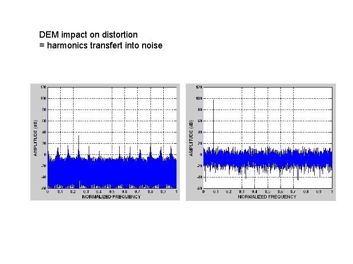
DEM impact on distortion = harmonics transfert into noise

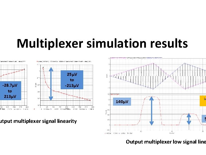
Multiplexer simulation results -28. 7µV to 213µV 25µV to -213µV utput multiplexer signal linearity 140µV Lo 5 Output multiplexer low signal line

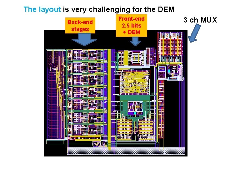
The layout is very challenging for the DEM Back-end stages Front-end 2. 5 bits + DEM 3 ch MUX

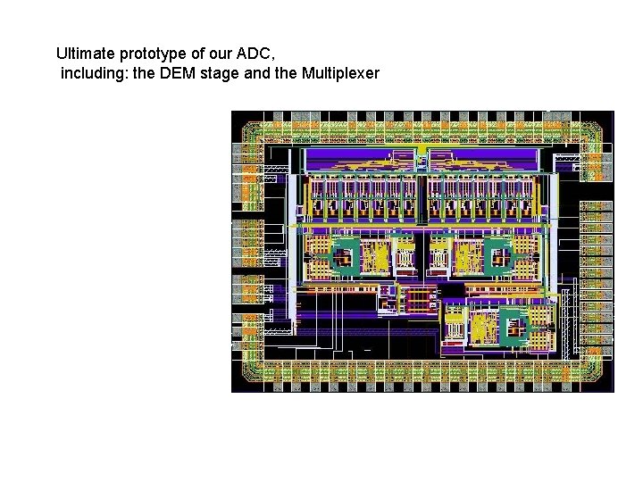
Ultimate prototype of our ADC, including: the DEM stage and the Multiplexer

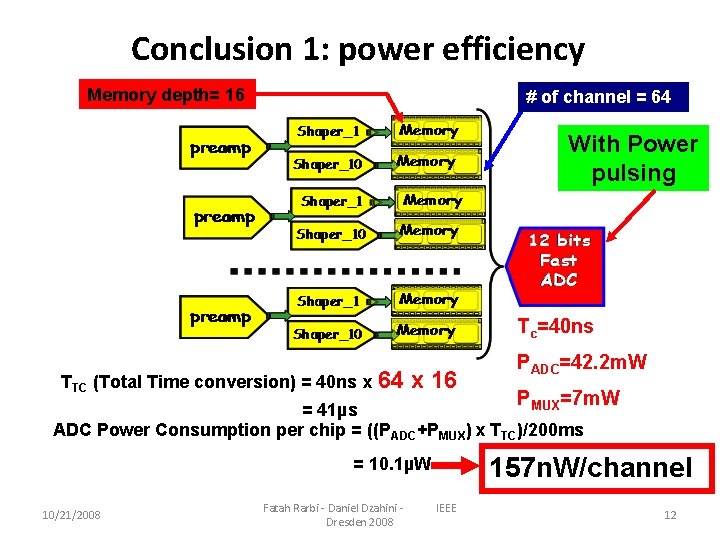
Conclusion 1: power efficiency Memory depth= 16 # of channel = 64 With Power pulsing Tc=40 ns TTC (Total Time conversion) = 40 ns x 64 x 16 PADC=42. 2 m. W P =7 m. W MUX = 41µs ADC Power Consumption per chip = ((PADC+PMUX) x TTC)/200 ms 157 n. W/channel = 10. 1µW 10/21/2008 Fatah Rarbi - Daniel Dzahini Dresden 2008 IEEE 12

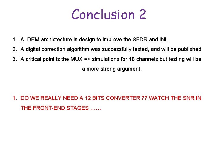
Conclusion 2 1. A DEM archictecture is design to improve the SFDR and INL 2. A digital correction algorithm was successfully tested, and will be published 3. A critical point is the MUX => simulations for 16 channels but testing will be a more strong argument. 1. DO WE REALLY NEED A 12 BITS CONVERTER ? ? WATCH THE SNR IN THE FRONT-END STAGES ……