CENG 4480A 3 AnalogDigital Conversions Analog to Digital
![Diagram of a flash ADC [1] AD/DA (v. 5 b) 29 Diagram of a flash ADC [1] AD/DA (v. 5 b) 29](https://slidetodoc.com/presentation_image_h/e0728a248775e00b6ac9847db5a11c31/image-29.jpg)
![Diagram of a subranging Flash built from two 4 -bit flash ADC, [1] § Diagram of a subranging Flash built from two 4 -bit flash ADC, [1] §](https://slidetodoc.com/presentation_image_h/e0728a248775e00b6ac9847db5a11c31/image-32.jpg)
![References § [1] Interfacing: A Laboratory Approach Using the Microcomputer for Instrumentation, Data Analysis, References § [1] Interfacing: A Laboratory Approach Using the Microcomputer for Instrumentation, Data Analysis,](https://slidetodoc.com/presentation_image_h/e0728a248775e00b6ac9847db5a11c31/image-49.jpg)
- Slides: 49

CENG 4480_A 3 Analog/Digital Conversions Analog to Digital (AD), Digital to Analog (DA) conversion AD/DA (v. 5 b) 1

Analog/digital conversions § Topics l l l Digital to analog conversion Analog to digital conversion Sampling-speed limitation Frequency aliasing Practical ADCs of different speed AD/DA (v. 5 b) 2

Digital to Analogue Conversion DAC AD/DA (v. 5 b) 3

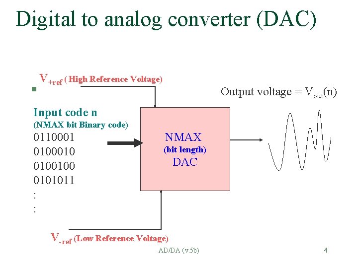
Digital to analog converter (DAC) § V+ref ( High Reference Voltage) Output voltage = Vout(n) Input code n (NMAX bit Binary code) 0110001 0100010 0100100 0101011 : : NMAX (bit length) DAC V-ref (Low Reference Voltage) AD/DA (v. 5 b) 4

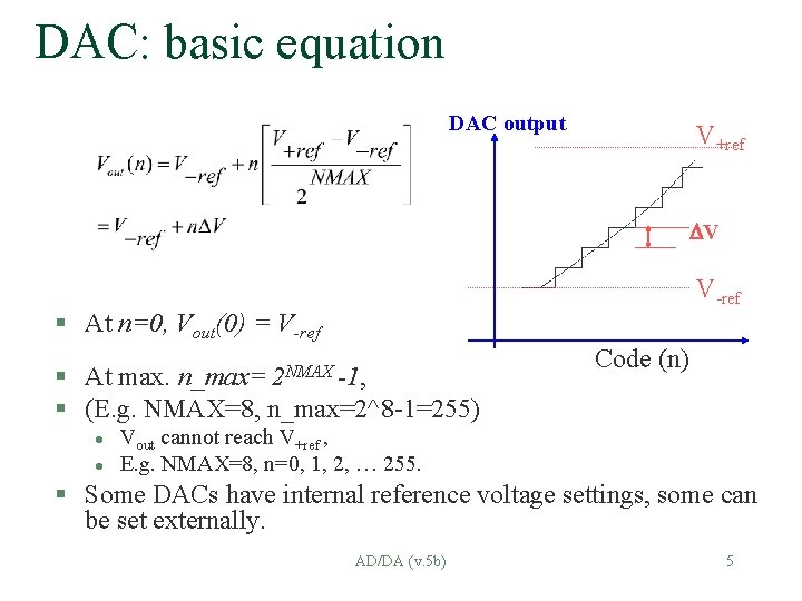
DAC: basic equation DAC output V+ref V V-ref § At n=0, Vout(0) = V-ref § At max. § (E. g. NMAX=8, n_max=2^8 -1=255) n_max= 2 NMAX -1, l l Code (n) Vout cannot reach V+ref , E. g. NMAX=8, n=0, 1, 2, … 255. § Some DACs have internal reference voltage settings, some can be set externally. AD/DA (v. 5 b) 5

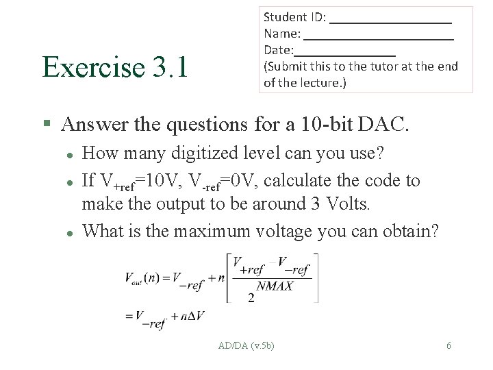
Exercise 3. 1 Student ID: _________ Name: ___________ Date: ________ (Submit this to the tutor at the end of the lecture. ) § Answer the questions for a 10 -bit DAC. l l l How many digitized level can you use? If V+ref=10 V, V-ref=0 V, calculate the code to make the output to be around 3 Volts. What is the maximum voltage you can obtain? AD/DA (v. 5 b) 6

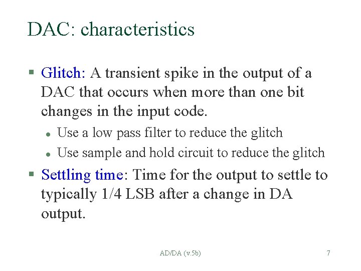
DAC: characteristics § Glitch: A transient spike in the output of a DAC that occurs when more than one bit changes in the input code. l l Use a low pass filter to reduce the glitch Use sample and hold circuit to reduce the glitch § Settling time: Time for the output to settle to typically 1/4 LSB after a change in DA output. AD/DA (v. 5 b) 7

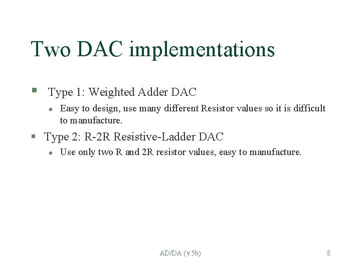
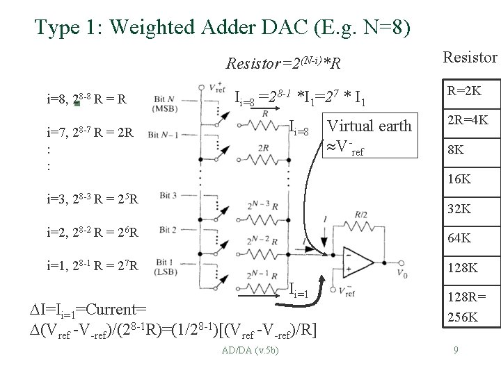
Two DAC implementations § Type 1: Weighted Adder DAC l Easy to design, use many different Resistor values so it is difficult to manufacture. § Type 2: R-2 R Resistive-Ladder DAC l Use only two R and 2 R resistor values, easy to manufacture. AD/DA (v. 5 b) 8

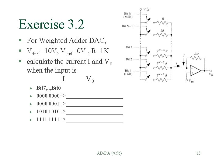
Type 1: Weighted Adder DAC (E. g. N=8) Resistor=2(N-i)*R Resistor i=8, 28 -8 R = R Ii=8 =28 -1 *I 1=27 * I 1 R=2 K 28 -7 R Ii=8 2 R=4 K § i=7, : : = 2 R Virtual earth V-ref 8 K 16 K i=3, 28 -3 R = 25 R 32 K i=2, 28 -2 R = 26 R 64 K i=1, 28 -1 R = 27 R 128 K Ii=1 I=Ii=1=Current= (Vref -V-ref)/(28 -1 R)=(1/28 -1)[(Vref -V-ref)/R] AD/DA (v. 5 b) 128 R= 256 K 9

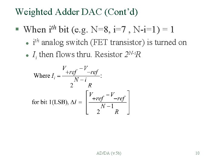
Weighted Adder DAC (Cont’d) § When ith bit (e. g. N=8, i=7 , N-i=1) = 1 l l ith analog switch (FET transistor) is turned on Ii then flows thru. Resistor 2 N-i. R AD/DA (v. 5 b) 10

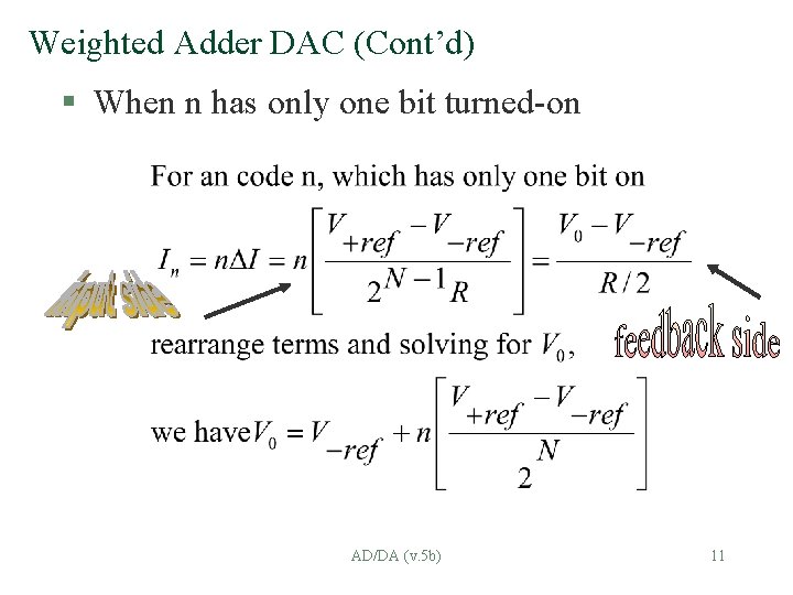
Weighted Adder DAC (Cont’d) § When n has only one bit turned-on AD/DA (v. 5 b) 11

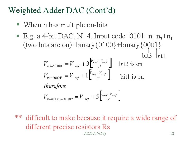
Weighted Adder DAC (Cont’d) § When n has multiple on-bits § E. g. a 4 -bit DAC, N=4. Input code=0101=n=n 3+n 1 (two bits are on)=binary{0100}+binary{0001} bit 3 bit 1 bit 3 is on bit 1 is on ** difficult to make because it require a wide range of different precise resistors Rs AD/DA (v. 5 b) 12

Exercise 3. 2 § For Weighted Adder DAC, § V+ref=10 V, V-ref=0 V , R=1 K § calculate the current I and V 0 when the input is I V 0 l l l Bit 7, . . , Bit 0 0000=>___________ 0000 0001=>___________ 1010=>___________ 1111=>___________ AD/DA (v. 5 b) 13

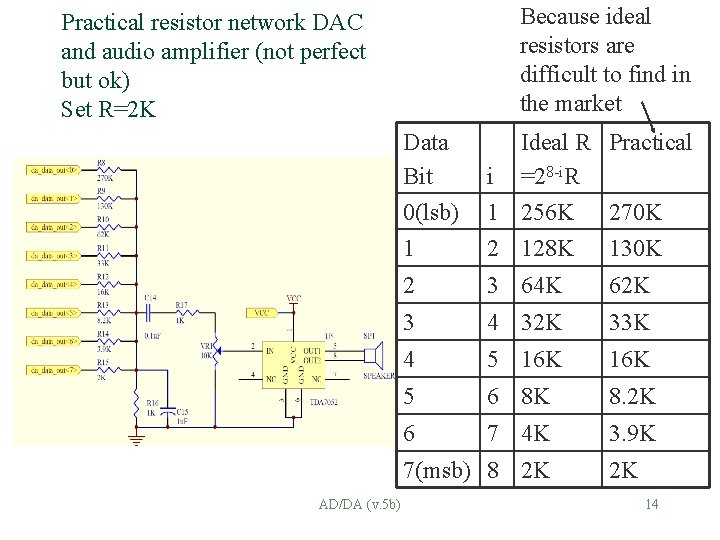
Because ideal resistors are difficult to find in the market Practical resistor network DAC and audio amplifier (not perfect but ok) Set R=2 K § Data Bit 0(lsb) 1 Ideal R Practical i =28 -i. R 1 256 K 270 K 2 128 K 130 K 2 3 64 K 62 K 3 4 32 K 33 K 4 5 16 K 5 6 8 K 8. 2 K 6 7 4 K 3. 9 K 7(msb) 8 2 K AD/DA (v. 5 b) 2 K 14

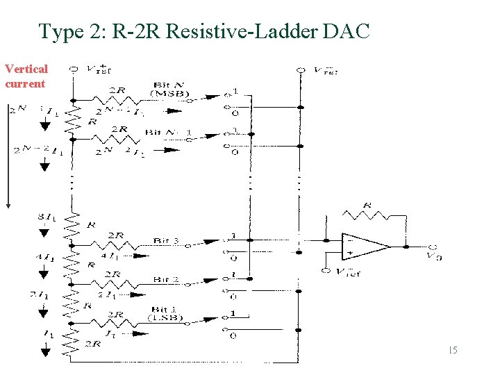
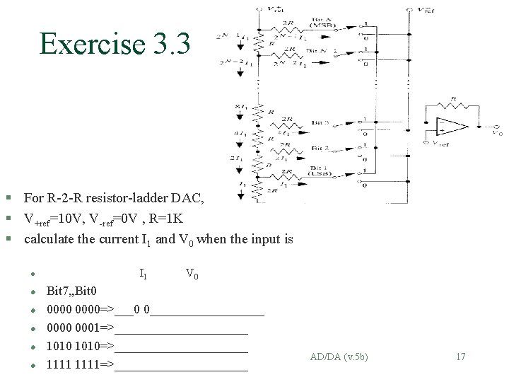
Type 2: R-2 R Resistive-Ladder DAC Vertical current AD/DA (v. 5 b) 15

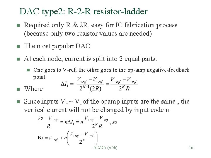
DAC type 2: R-2 -R resistor-ladder n Required only R & 2 R, easy for IC fabrication process (because only two resistor values are needed) n The most popular DAC n At each node, current is split into 2 equal parts: n One goes to V-ref; the other goes to the op-amp negative-feedback point n Where n Since inputs V+ ~ V- of the opamp inputs are the same , the vertical current will not be changed by input code n AD/DA (v. 5 b) 16

Exercise 3. 3 § For R-2 -R resistor-ladder DAC, § V+ref=10 V, V-ref=0 V , R=1 K § calculate the current I 1 and V 0 when the input is l l l I 1 V 0 Bit 7, , Bit 0 0000=>___0 0_________ 0000 0001=>___________ 1010=>___________ 1111=>___________ AD/DA (v. 5 b) 17

Analog to Digital Conversion ADC AD/DA (v. 5 b) 18

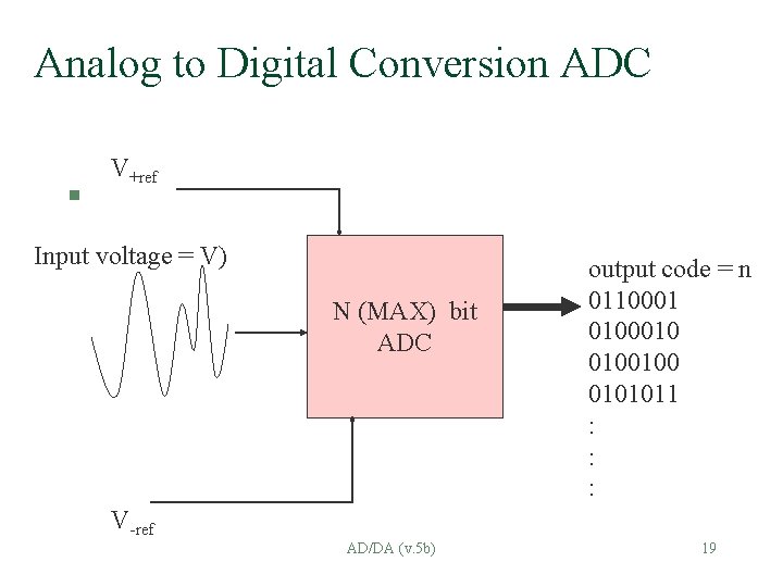
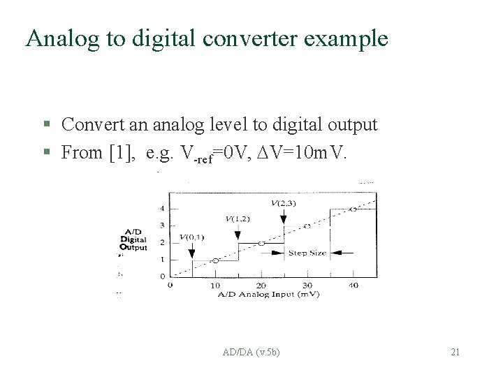
Analog to Digital Conversion ADC § V+ref Input voltage = V) N (MAX) bit ADC output code = n 0110001 0100010 0100100 0101011 : : : V-ref AD/DA (v. 5 b) 19

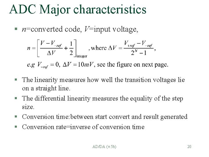
ADC Major characteristics § n=converted code, V=input voltage, § The linearity measures how well the transition voltages lie on a straight line. § The differential linearity measures the equality of the step size. § Conversion time: between start convert and result generated § Conversion rate=inverse of conversion time AD/DA (v. 5 b) 20

Analog to digital converter example § Convert an analog level to digital output § From [1], e. g. V-ref=0 V, V=10 m. V. AD/DA (v. 5 b) 21

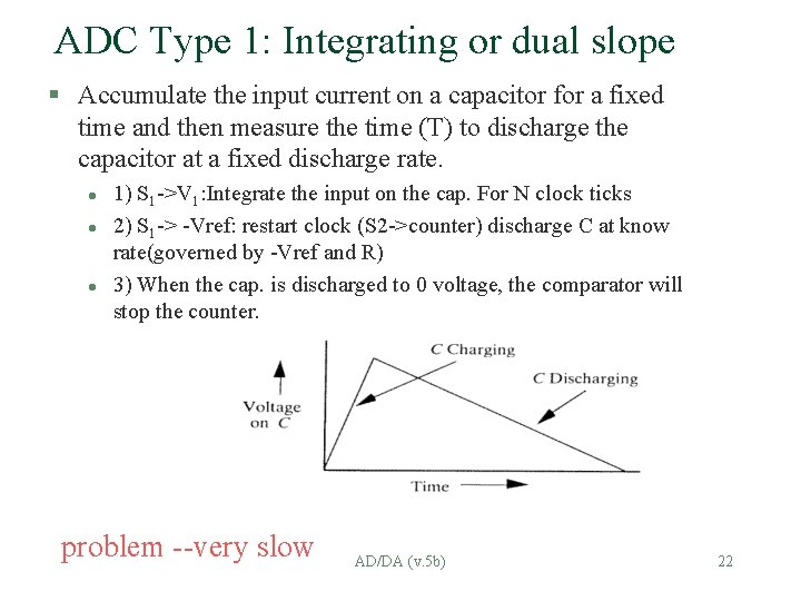
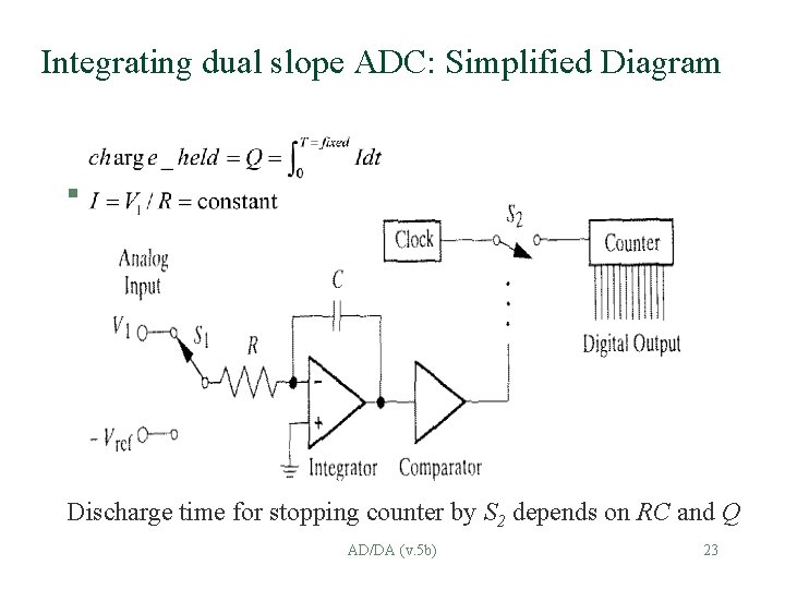
ADC Type 1: Integrating or dual slope § Accumulate the input current on a capacitor for a fixed time and then measure the time (T) to discharge the capacitor at a fixed discharge rate. l l l 1) S 1 ->V 1: Integrate the input on the cap. For N clock ticks 2) S 1 -> -Vref: restart clock (S 2 ->counter) discharge C at know rate(governed by -Vref and R) 3) When the cap. is discharged to 0 voltage, the comparator will stop the counter. problem --very slow AD/DA (v. 5 b) 22

Integrating dual slope ADC: Simplified Diagram § Discharge time for stopping counter by S 2 depends on RC and Q AD/DA (v. 5 b) 23

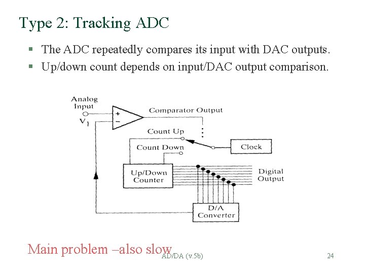
Type 2: Tracking ADC § The ADC repeatedly compares its input with DAC outputs. § Up/down count depends on input/DAC output comparison. Main problem –also slow AD/DA (v. 5 b) 24

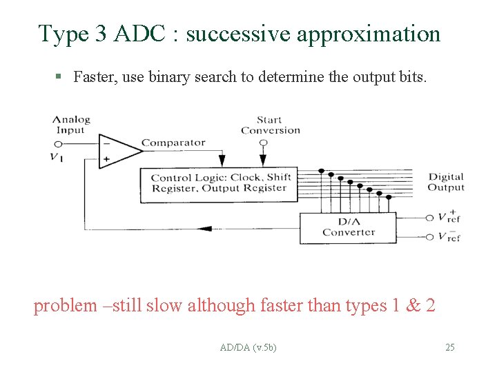
Type 3 ADC : successive approximation § Faster, use binary search to determine the output bits. problem –still slow although faster than types 1 & 2 AD/DA (v. 5 b) 25

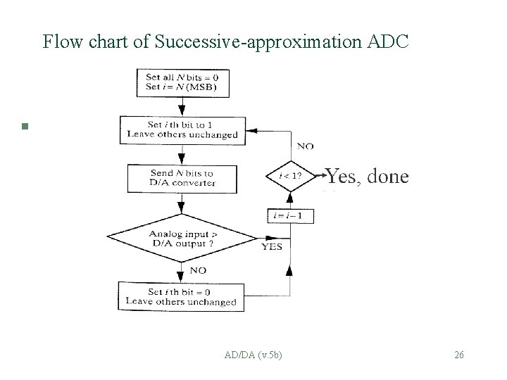
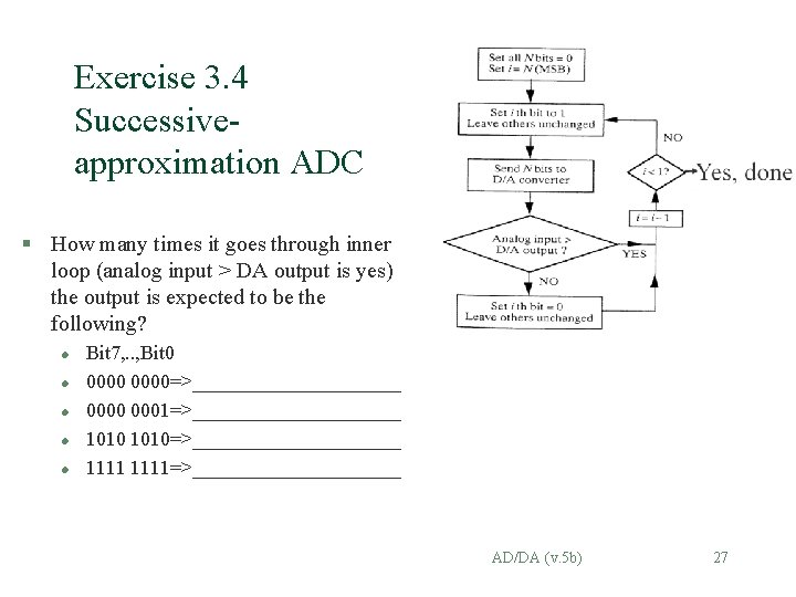
Flow chart of Successive-approximation ADC § AD/DA (v. 5 b) 26

Exercise 3. 4 Successiveapproximation ADC § How many times it goes through inner loop (analog input > DA output is yes) if the output is expected to be the following? l l l Bit 7, . . , Bit 0 0000=>___________ 0000 0001=>___________ 1010=>___________ 1111=>___________ AD/DA (v. 5 b) 27

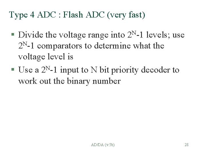
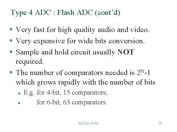
Type 4 ADC : Flash ADC (very fast) § Divide the voltage range into 2 N-1 levels; use 2 N-1 comparators to determine what the voltage level is § Use a 2 N-1 input to N bit priority decoder to work out the binary number AD/DA (v. 5 b) 28
![Diagram of a flash ADC 1 ADDA v 5 b 29 Diagram of a flash ADC [1] AD/DA (v. 5 b) 29](https://slidetodoc.com/presentation_image_h/e0728a248775e00b6ac9847db5a11c31/image-29.jpg)
Diagram of a flash ADC [1] AD/DA (v. 5 b) 29

Type 4 ADC : Flash ADC (cont’d) § Very fast for high quality audio and video. § Very expensive for wide bits conversion. § Sample and hold circuit usually NOT required. § The number of comparators needed is 2 N-1 which grows rapidly with the number of bits l l E. g. for 4 -bit, 15 comparators; for 6 -bit, 63 comparators. AD/DA (v. 5 b) 30

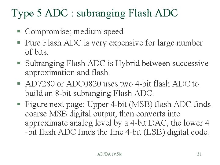
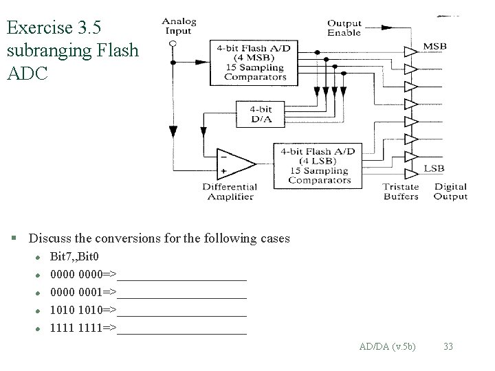
Type 5 ADC : subranging Flash ADC § Compromise; medium speed § Pure Flash ADC is very expensive for large number of bits. § Subranging Flash ADC is Hybrid between successive approximation and flash. § AD 7280 or ADC 0820 uses two 4 -bit flash ADC to build an 8 -bit subranging Flash ADC. § Figure next page: Upper 4 -bit (MSB) flash ADC finds coarse MSB digital output, then converts into approximate analog level by a 4 -bit DAC, the lower 4 -bit flash ADC finds the fine 4 -bit (LSB) digital code. AD/DA (v. 5 b) 31
![Diagram of a subranging Flash built from two 4 bit flash ADC 1 Diagram of a subranging Flash built from two 4 -bit flash ADC, [1] §](https://slidetodoc.com/presentation_image_h/e0728a248775e00b6ac9847db5a11c31/image-32.jpg)
Diagram of a subranging Flash built from two 4 -bit flash ADC, [1] § AD/DA (v. 5 b) 32

Exercise 3. 5 subranging Flash ADC § Discuss the conversions for the following cases l l l Bit 7, , Bit 0 0000=>___________ 0000 0001=>___________ 1010=>___________ 1111=>___________ AD/DA (v. 5 b) 33

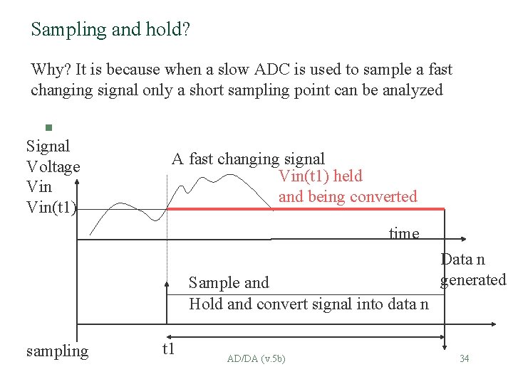
Sampling and hold? Why? It is because when a slow ADC is used to sample a fast changing signal only a short sampling point can be analyzed § Signal Voltage Vin(t 1) A fast changing signal Vin(t 1) held and being converted time Sample and Hold and convert signal into data n sampling t 1 AD/DA (v. 5 b) Data n generated 34

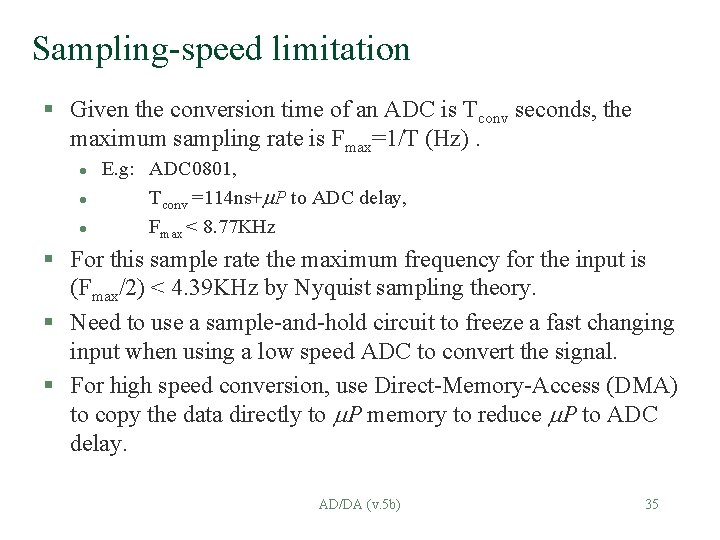
Sampling-speed limitation § Given the conversion time of an ADC is Tconv seconds, the maximum sampling rate is Fmax=1/T (Hz). l l l E. g: ADC 0801, Tconv =114 ns+ P to ADC delay, Fmax < 8. 77 KHz § For this sample rate the maximum frequency for the input is (Fmax/2) < 4. 39 KHz by Nyquist sampling theory. § Need to use a sample-and-hold circuit to freeze a fast changing input when using a low speed ADC to convert the signal. § For high speed conversion, use Direct-Memory-Access (DMA) to copy the data directly to P memory to reduce P to ADC delay. AD/DA (v. 5 b) 35

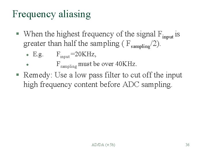
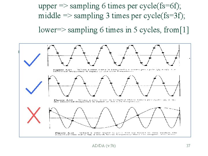
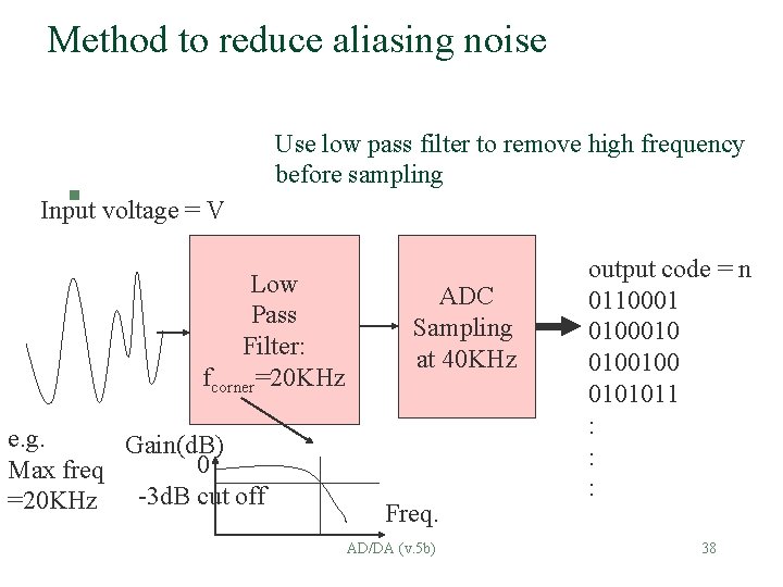
Frequency aliasing § When the highest frequency of the signal Finput is greater than half the sampling ( Fsampling/2). l l E. g. Finput =20 KHz, Fsampling must be over 40 KHz. § Remedy: Use a low pass filter to cut off the input high frequency content before ADC sampling. AD/DA (v. 5 b) 36

upper => sampling 6 times per cycle(fs=6 f); middle => sampling 3 times per cycle(fs=3 f); lower=> sampling 6 times in 5 cycles, from[1] § AD/DA (v. 5 b) 37

Method to reduce aliasing noise § voltage = V Input Use low pass filter to remove high frequency before sampling Low Pass Filter: fcorner=20 KHz e. g. Gain(d. B) 0 Max freq -3 d. B cut off =20 KHz ADC Sampling at 40 KHz Freq. AD/DA (v. 5 b) output code = n 0110001 0100010 0100100 0101011 : : : 38

Exercise 3. 6 § If a signal is ranging from 30 Hz to 100 KHz, what is the suitable sampling rate for the ADC to be used. § Answer: ______________ § If noise exists in the surrounding, what should you do to ensure the conversion is accurate? § Answer: _____________ AD/DA (v. 5 b) 39

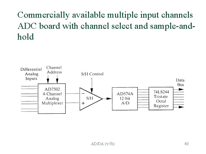
Commercially available multiple input channels ADC board with channel select and sample-andhold AD/DA (v. 5 b) 40

Practical ADCs § Low cost, low speed (successive approximation, 8 bit-8 KHz sampling), National semiconductor ADC 0801, 2, 3, 4 family. See http: //www. national. com/catalog/ § Medium speed (half-flash, 8 -bit 666 KHz), National semiconductor ADC 0820. § High speed (flash 8 -bit, 40 80 MHz, video quality) Philips TDA 8714 (/7/6/4) family. See http: //207. 87. 19. 21/products/ AD/DA (v. 5 b) 41

ADC 0801 description from http: //www. national. com/catalog/ § 8 -bit successive approximation A/D converters that use a differential potentiometric ladder-similar to the 256 R products. § Output latches directly driving the data bus. § These A/Ds appear like memory locations or I/O ports to the microprocessor and no interfacing logic is needed. § Differential analog voltage inputs allow increasing the common-mode rejection and offsetting the analog zero input voltage value. § Voltage reference input can be adjusted to allow encoding any smaller analog voltage span to the full 8 bits of resolution. AD/DA (v. 5 b) 42

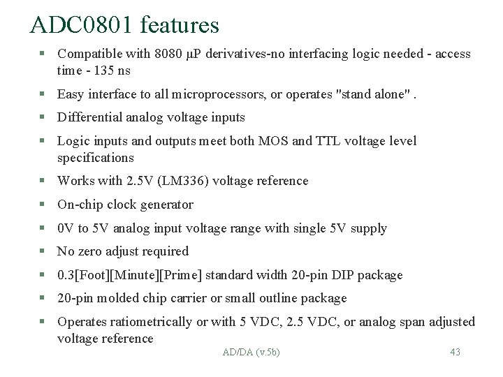
ADC 0801 features § Compatible with 8080 µP derivatives-no interfacing logic needed - access time - 135 ns § Easy interface to all microprocessors, or operates "stand alone". § Differential analog voltage inputs § Logic inputs and outputs meet both MOS and TTL voltage level specifications § Works with 2. 5 V (LM 336) voltage reference § On-chip clock generator § 0 V to 5 V analog input voltage range with single 5 V supply § No zero adjust required § 0. 3[Foot][Minute][Prime] standard width 20 -pin DIP package § 20 -pin molded chip carrier or small outline package § Operates ratiometrically or with 5 VDC, 2. 5 VDC, or analog span adjusted voltage reference AD/DA (v. 5 b) 43

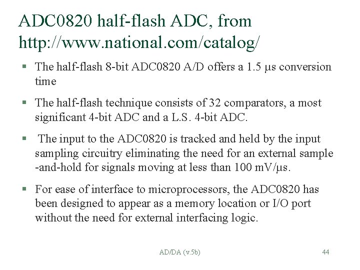
ADC 0820 half-flash ADC, from http: //www. national. com/catalog/ § The half-flash 8 -bit ADC 0820 A/D offers a 1. 5 µs conversion time § The half-flash technique consists of 32 comparators, a most significant 4 -bit ADC and a L. S. 4 -bit ADC. § The input to the ADC 0820 is tracked and held by the input sampling circuitry eliminating the need for an external sample -and-hold for signals moving at less than 100 m. V/µs. § For ease of interface to microprocessors, the ADC 0820 has been designed to appear as a memory location or I/O port without the need for external interfacing logic. AD/DA (v. 5 b) 44

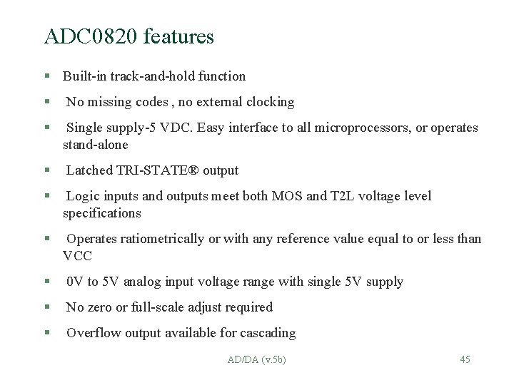
ADC 0820 features § Built-in track-and-hold function § No missing codes , no external clocking § Single supply-5 VDC. Easy interface to all microprocessors, or operates stand-alone § Latched TRI-STATE® output § Logic inputs and outputs meet both MOS and T 2 L voltage level specifications § Operates ratiometrically or with any reference value equal to or less than VCC § 0 V to 5 V analog input voltage range with single 5 V supply § No zero or full-scale adjust required § Overflow output available for cascading AD/DA (v. 5 b) 45

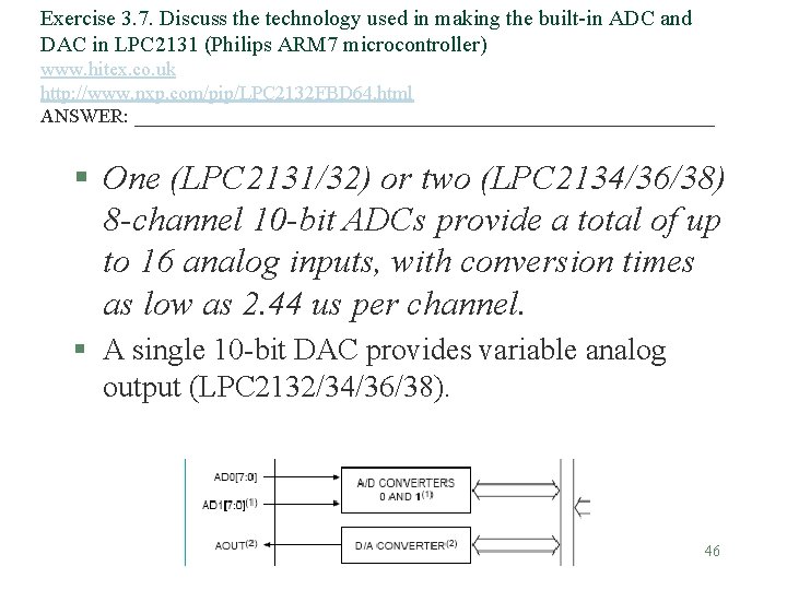
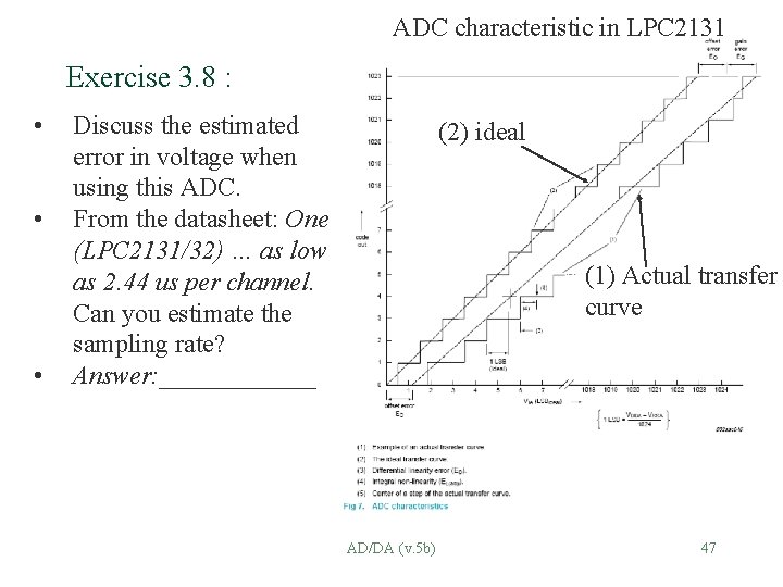
Exercise 3. 7. Discuss the technology used in making the built-in ADC and DAC in LPC 2131 (Philips ARM 7 microcontroller) www. hitex. co. uk http: //www. nxp. com/pip/LPC 2132 FBD 64. html ANSWER: ______________________________ § One (LPC 2131/32) or two (LPC 2134/36/38) 8 -channel 10 -bit ADCs provide a total of up to 16 analog inputs, with conversion times as low as 2. 44 us per channel. § A single 10 -bit DAC provides variable analog output (LPC 2132/34/36/38). AD/DA (v. 5 b) 46

ADC characteristic in LPC 2131 Exercise 3. 8 : • • • Discuss the estimated error in voltage when using this ADC. From the datasheet: One (LPC 2131/32) … as low as 2. 44 us per channel. Can you estimate the sampling rate? Answer: ______ (2) ideal (1) Actual transfer curve AD/DA (v. 5 b) 47

Summary § Studied the operations of Digital/analogue conversions. § Studied the application of Digital/analogue converters. AD/DA (v. 5 b) 48
![References 1 Interfacing A Laboratory Approach Using the Microcomputer for Instrumentation Data Analysis References § [1] Interfacing: A Laboratory Approach Using the Microcomputer for Instrumentation, Data Analysis,](https://slidetodoc.com/presentation_image_h/e0728a248775e00b6ac9847db5a11c31/image-49.jpg)
References § [1] Interfacing: A Laboratory Approach Using the Microcomputer for Instrumentation, Data Analysis, and Control by Stephen E. Derenzo § [2] http: //www. nxp. com/pip/LPC 2132 FBD 64. h tml AD/DA (v. 5 b) 49