Lec 13 Analog vs Digital Analog vs Digital


 memory")


 0 0 0 1 1 1 Accumulator (AC)")


 counts by trying")


")


- Slides: 37
Lec – 13
Analog vs Digital
Analog vs Digital
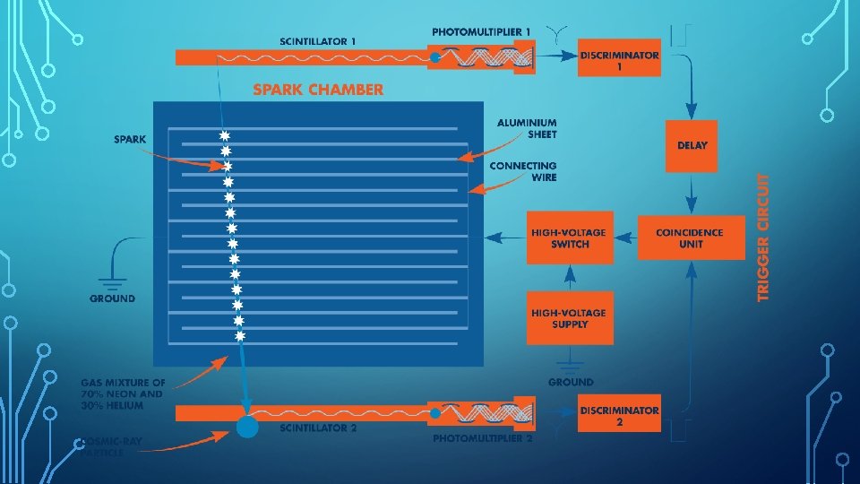
Atlas Detector - CERN
Atlas Detector - CERN
Analog vs Digital • Advantages of Analog: 1. Information is a continuous function, eg, a transducer, such as a temperature gauge outputs a voltage (or current) that is a continuous function of the temperature…the most potentially accurate information about the temperature is contained in the instantaneous value of the output voltage. 2. The information can be transmitted down a single cable, wire or channel (The phone company used to transmit this way). • Disadvantages of Analog: 1. It’s noisy… very susceptible to pickup of external noise that renders an analog signal inaccurate or at worst… unintelligible. 2. Signal degrades if transmitted via cable over long distances. • Advantages of Digital: 1. Noise immunity… normally a 0 might be defined as 0 V and a 1 as +5 V, but a signal is either 0 or 1 with relatively large noise margins, eg, a 0 could be any voltage between 0 – 0. 8 V and a 1 anything above 2 V. 2. Typically, signals are ‘cleaned up’ when they pass thru a following logic gate. 3. Allows transmission without error (mostly) but do have to deal with ‘round-off error’. 4. Data can be processed later…not necessarily in real time. (An experiment might take 1 year to gather data, but could be processed over a time frame of 100 years. 5. Digital circuitry makes computers possible (to be fair… there used to be such things as analog computers, which had their heyday for awhile in such applications as aircraft simulators).
THE DECIMAL CODE What does the number 3298 mean? It means three thousand two hundred and ninety-eight. Humans use the decimal code so frequently (possibly because we have ten fingers) and so unconsciously that most of us have forgotten that it is a place-based number based on powers of ten—or the decimal base. We owe this numbering system to Hindu scholars who invented it certainly by the 6 th century CE and possibly earlier. 105=100000 104=10000 103=1000 102=100 101=10 100=1 0 0 3 2 9 8 x 105 = x 104 = x 103 = x 102 = x 101 = x 100 = 000000 + 00000 + 3000 + 200 + 90 + 8 3298
THE BINARY CODE Numbers stored in computers use the base two, or binary system, which requires only 2 digits … 0 and 1. Why? Modern day computers are electronic gadgets. It’s loaded with tiny electronic switches, which either allow the passage of electrical current or block its passage. Can 3298 be represented as a binary number, which in turn is represented by the physical state of twelve switches? 211= 2048 210= 1024 29 = 512 28 = 256 27 = 128 26 = 64 25 = 32 24 = 16 23 = 8 22 = 4 21 = 2 20 = 1 1 1 0 0 0 1 0 Switch closed = “ 1” Switch open = “ 0”
BINARY REPRESENTATION OF 329810 The binary number this pattern of switch states represents is— 1100111000102 Binary Digit (Bit) 1 1 0 0 1 1 1 0 0 0 1 0 Place Value x 211= x 210= x 29= x 28= x 27= x 26= x 25= x 24= x 23= x 22= x 21= x 20= Binary Number 10000000000 00000 10000000 1000000 100000 000 10 0 110011100010 Decimal Number 2048 1024 0 0 128 64 32 0 0 0 2 0 3298 By the way…a binary digit is called a bit
IS INFORMATION NOTHING BUT BITS? How does a computer add two numbers together? Duh…how much is 7 + 5 ? • Computers run programs - a sequence of instructions and data designed to carry out some algorithm - a sequence of steps required to perform some kind of calculation or answer some question. • Some human wrote the program and ‘put it inside the computer’ so that it could execute the instructions using the data supplied and arrive at an answer— presumably faster than could be accomplished by its human programmer. How does this work?
A ‘COMPUTER FOR DUMMIES’ A basic computer consists of two main parts: (i) memory and a (ii) CPU, or central processing unit.
MEMORY • Memory is where all information is stored in the computer. It consists of a ‘matrix’ of electronic switches arranged in a sequence of cells whose rows represent computer ‘words’. • In our ‘computer for dummies’, each word is represented by a 8 switches in a row that can be either off or on-each representing a 0 or 1 (historically, a ‘byte’ is ½ of a word. If a computer operates with 16 bit words, each word consists of two bytes—each byte is then 8 bits long). • Words are arranged in sequential rows and the location of the row in which a word resides is designated by a number, which is the address of the word. This arrangement is depicted in following table.
COMPUTER MEMORY-A STACK OF SWITCHES Memory Address 0 0 0 1 0 0 2 0 0 3 0 0 4 0 0 5 0 0 …etc 0 0 0 0 0 0 0 1 0 0 0 1 1 1 0 0 0 1 0 1 0 0 Each 8 -bit word (here a byte is equivalent to a word) has an address from 0 → some max, say 1 Gigabyte Each word is simply a set of 8 electronic switches-some off and some on
COMPUTER CPU • The CPU is ‘driven’ by an electronic oscillator ‘clock’. The CPU consists of a lot of electronics that turns switches on or off as needed—at a rate determined by the frequency of the clock. If that frequency is, say, 3 gigahertz (Ghz), the clock ticks at a rate of 3 billion cycles per second. • Our ‘computer for dummies’ has 2 essential parts —two electronic registers — the accumulator and the program counter. • The accumulator does what its name implies—it accumulates—or stores the intermediate results of some calculation in progress. • The program counter (PC) keeps track of where you are in the program— that is, which step in the program is currently being executed.
PC AND ACCUMULATOR Program Counter (PC) 0 0 0 1 1 1 Accumulator (AC) 0 0 0 Registers, like memory, are an array of 8 electronic switches - as in memory (but they’re made differently and can change state much faster). At the moment, the binary number 11 shown in the program counter is equivalent to decimal 3. This means that whatever ‘information’ is stored at memory address 3 is about to be retrieved, or fetched, from that memory location and ‘operated with or upon’ by the CPU. The binary number 111, or decimal 7, currently is in the accumulator. It will be overwritten with the result of the CPU’s current operation. The CPU will then automatically increment the contents of the PC by 1 obtaining the binary number 100, or decimal 4. The CPU will now retrieve whatever ‘information’ is stored at memory address location 4 and operate upon it, storing the new result in the AC.
PROGRAM TO ADD 7 + 5 Memory Address 0 0 1 0 0 0 2 0 0 0 3 0 0 0 4 0 0 0 5 0 0 0 …etc 0 0 0 0 0 1 0 0 0 1 1 1 0 0 0 1 0 1 0 0 Instruction Clear AC Add #7, AC 7 Add #5, AC 5 Halt Every computer program is written in binary code. A given binary number represents one of the many instructions to which the computer has been constructed to ‘recognize. ’ The program above uses only two (of many possible) instructions. The PC is ‘zeroed’ to start. The CPU ‘fetches’ the binary number located at memory address 0 and ‘decodes’ this number—its value is 1— representing the instruction—‘clear the accumulator’
Memory Address 0 0 1 0 0 0 2 0 0 0 3 0 0 0 4 0 0 0 5 0 0 0 …etc 0 0 0 0 0 1 0 0 0 1 1 1 0 0 0 1 0 1 0 0 Instruction Clear AC Add #7, AC 7 Add #5, AC 5 Halt • The CPU then increments the PC to 1—goes to memory location 1— fetches the number from that location—decodes it—realizes that the binary number 10 (decimal 2) means ‘add #7 to the AC. ’ • Furthermore, the CPU knows that the number to be added to the accumulator (which is 7) is located at the next sequential memory address, immediately following the add instruction. • We have colored the 7 red to indicate that this binary number is data and not an instruction—it doesn’t have to be decoded. The CPU knows that this is the situation that applies to every add # instruction—the data always follows immediately after the instruction (the # symbol stands for immediate).
Memory Address 0 0 1 0 0 0 2 0 0 0 3 0 0 0 4 0 0 0 5 0 0 0 …etc 0 0 0 0 0 1 0 0 0 1 1 1 0 0 0 1 0 1 0 0 Instruction Clear AC Add #7, AC 7 Add #5, AC 5 Halt • The CPU again increments the PC … this time from 1 to 2— goes to memory location 2—fetches the data and, no need to decode, simply adds that data to the accumulator. Thus, 111, or decimal 7 is now stored in the accumulator. • The process continues until the CPU fetches all 0’s at memory location 5—decodes the instruction, which means halt—and so the computer halts. I bet that you can now see that the value stored in the AC is 1100, or decimal 12, which is the correct answer.
WHY ANALOG IS DISAPPEARING • Eg, Commercial Audio … CD’s, etc. • Uses 16 -bit A/D to ‘encode’ A … then 16 bit D/A to ‘decode’ • Let’s say max signal ~ 5 V. 16 bit A/D slices voltage into 216 or 65, 536 slices, each slice ~ 76 μV. • Not much information lost • Clearly…increasing the number of bits increases clarity of signal although I have heard a rumor that real ‘audiophiles’ turn their noses (or rather ears) up at digital audio!
Example - Successive Approximation A/D • A successive approximation register (SAR) counts by trying all values of bits starting with the MSB and finishing at the LSB. • Throughout the count process, the register monitors the comparator’s output to see if the DAC, driven by the binary output of the SAR, produces a voltage less than or greater than the analog signal input, adjusting the bit values accordingly. • Usually, a sample and hold circuit precedes the comparator so that Vin is stable during the conversion process. • Also, there is logic circuitry to produce a start and stop command that is not shown here. • Schematic of an (i) input signal (ii) the SAR output as it converges on the input and (iii) the latched output upon completion of a conversion cycle.
Number Codes 1. Hexadecimal: 0 – 9 = 0 – 9, 10 – 15 = A – F, eg, 70710 = 10110000112 (= 10 1100 00112) = 2 C 316. • Commonly used when doing a computer ‘core dump’ to read exactly what’s stored in memory. • Eg, 16, 32 and 64 – bit computer words consist of 2, 4 and 8 bytes or 4, 8 and 16 hex digits. 2. Binary-Coded Decimal: Each decimal digit is coded into binary requiring 4 bits for each digit (See HW_3, Problem 1). BCD NEVER represents any digit whose value > 9! • Eg, π = 3143… = 0011 0001 0100 0011 … • If a computer is going to ultimately spit out numbers for humans to read, it performs a binary to BCD decoding operation (non-trivial)…then it trivially decodes BCD to decimal. Integer 2’s Comp +7 0111 +6 0110 +5 0101 +4 0100 +3 0011 +2 0010 +1 0001 0 0000 -1 1111 -2 1110 -3 1101 -4 3. 2’s Complement: The negative number that you add to any binary number to get 0 is the 2’s complement of that number. • To calculate –ve numbers in 2’s complement: (i) Complement all the bits in the number N to get N*; (ii) Add 1 to get –N = N* + 1…that is the 2’s complement. • Eg, The numbers -7 thru +7 require 4 bits; the -ve values will always have 1 as MSB. • Calculate 2’s comp of 7. (i) 710 = 01112 (ii) N* = 1000 (iii) -7 = N* + 1 = 1001 • Check… - 7 + 7 = 0111 + 1001 = 0000 • Example: What is 5 – 2 ? -2 = (complement +2 then add 1… 1101 +1 = 1110); +5 = 0101 +5 0101 1100 -2 1110 -5 1011 +3 0011 -6 1010 -7 1001
Gray Code • • • Used for linear and shaft angle encoders. Only 1 bit changes in going from one state to the next. Prevents potentially horrible errors in mechanical systems. If binary code used, several bits might change at once…but in mechanical systems, one might change a little before the other. If binary were used, going from 3 to 4 you might get a 7 instead (MSB changes from 0 → 1 before least 2 significant bits change from 1 → 0) • To generate a gray code…start with 0 then to get to next state, simply change only the single LSB that brings you to a new state…one that does not yet exist. • Gray codes are also used for ‘flash’ A/D’s … the fastest A/D technique.
Combinatorial vs Sequential Logic • 1. 2. 3. 4. 5. 6. Combinatorial Tasks: Add two numbers Compare two numbers Compute a “parity” bit Decode binary into decimal Detect a coincidence between two events Etc. • Can all be accomplished via gates. • 1. 2. 3. 4. 5. 6. Sequential Tasks: Converting serial string of bits into parallel Counting number of 1’s in a sequence Recognizing a pattern in a sequence Producing 1 output pulse after 4 input pulses Stepping through memory in a computer Etc. • Can be accomplished by ‘flip-flops’. Logic Gates Common. Symbols: AND OR NOT XOR A∙B A+B A* ( ) A B
de. Morgan’s Theorem • You can swap gates shapes IF at the same time, you invert all inputs and outputs. • The circuit at right is clearly a NAND. • The circuit at left is an NOR for LOW inputs…if we think of either input as TRUE when it is LOW, then the output is HIGH • Rethink the AND gate below … if we consider LOW to be TRUE • • • Why subject you to all this? The inputs of many gate families float HIGH Generating a TRUE condition requires pulling them LOW. • Sometimes you simply want to assert the truth of some condition by establishing a connection to ground.
Logic Gate Examples Example 1 … Consider the possibility of launching a nuclear missile towards some rogue nation. What should the fail safe condition look like? 1. ‘Wacko’ president must push a button that grounds an input to the launch trigger. 2. At the same time equally ‘Wacko’ Chairman of the JCS must ground another input at the same time to launch the missile… Example 2 • Guess what? . . . Prob 1, HW_ 6 • What goes in the Logic… • even if the decision is illogical?
Logic Gate Examples Example 3 … You wish to sound a buzzer (BUZZ = HIGH) if a driver is seated in a car and either of the doors is open (it’s a 2 -door car). A • Solution: Best to restate the problem… • Output HIGH if either the right door or left door is HIGH and the driver is HIGH, i. e. , Q = (L+R)∙S • Looks like OR gate followed by AND gate will work… • But…Switches will probably close a circuit to ground…In other words, we want ‘active’ LOWS ! If both L and R are High, doors are closed! • Logical condition required is… • Make L* and R* inputs to AND gate then if either input is LOW…output is LOW. • When EITHER* is LOW, If driver is seated, S* is LOW. • Follow AND with NOR…output will be HIGH if driver seated • Note…you could use de. Morgan’s theorem to replace Fig B with the gates shown in Fig C. These gates generate the identical truth table, but they make much more clear the use of LOW true logic. • Also note, Fig C is identical to Fig A…if logic is LOW true. B Bzz 0 0 0 1 0 1 0 0 1 1 1 0 C
TTL and CMOS Logic Gates LS TTL NAND Inputs float HIGH CMOS NAND followed by a CMOS NOT • TTL NAND: (i) Diode – resistor logic drives Q 1 inverter, which (ii) drives a push – pull output. • If both inputs HI, Q 1 on, which saturates Q 4. • If either input LO, Q 1 off and Q 2, Q 3 on making output HI. • For CMOS NAND, both inputs must be HI to turn on Q 3, Q 4 and turn off Q 1, Q 2 producing a LO. • Q 5, Q 6 invert the LO to make a HI. • Guaranteed HIGHs, LOWs: • (2. 4, 0. 4) V for TTL output • (2. 0, 0. 8) V for TTL input • (4. 9, 0. 1) V for CMOS output • (3. 5, 1. 0) V for CMOS input • 1. 2. Why active LOWS are mostly used… TTL LO more vulnerable to noise (leave it HI). TTL HI easy to drive…(it floats HI).
Simplified MOSFET Symbols - Continued • Shown here are two mosfets, P-channel (Q 1) and N-channel (Q 2), hooked together as a CMOS (Complementary MOS) pair. 1) You cannot tell from these symbols whether or not they are enhancement mode (normally OFF) or depletion mode (normally ON). 2) Assume that they are enhancement mode, i. e. , if there is 0 V between Gate and Source…they are NOT conducting…they are OFF! 3) To get them to conduct, you need to make VGS < 0 V for P-channel (Q 1) and VGS > 0 V for N-channel (Q 2). 4) The arrow always denotes the source and if it points away from the gate…it’s N-channel (Q 2). 5) If the arrow points toward the gate…it’s P-channel (Q 1).
Noise Immunity Test • When noise is not too severe, all families pass. • The failures begin to show up on low level inputs when noise is increased. • 1 st 74 LS and 74 HCT (CMOS designed to work with TTL) • Then 74 HC (CMOS) fails with a lot of noise added. • 74 HC 14 doesn’t fail…uses Schmitt trigger with hysteresis.
Low Voltage Differential Signaling • Supply Voltage for LVDS is +1. 8 V • Uses differential drivers and receivers for transmission. • Driver transmits currents. • Receiver has input resistor that converts differential current into 0. 35 V. • Input to driver was 5 V TTL • 1 V triangular wave injected into ground terminal of driver, which caused 1 V common mode ‘noise’ on driver output lines. You can see 0. 35 V differential output buried in 1 V common mode noise. • Differential receiver rejects common mode noise and extracts the 0. 35 V transmission…and converts it back to 5 V TTL output.
Speed vs Power Dissipation Low Voltage Differential Signalling LVDS Power dissipation depends on supply voltage and switching frequency: P = Cpd VCC 2 f, where is the ‘power dissipation capacitance’.
Open Collector vs Three-State • Can’t do a ‘wired – OR’ with 3 -state. • Open Collector useful in computers to attach ‘peripherals’ to a single ‘bus’ line to generate an ‘interrupt’… • ‘Look at me’ Open Collector (Drain) • • Tri-State (3 -State) … the name is misleading! It is NOT digital logic with 3 voltage levels. It is ordinary logic (low & high) … but with a 3 rd output state that is open-circuit. It has a separate input which is used to enable whether the output behaves like an ordinary active pullup or goes into the “ 3 rd” (open) state. • Thus, when enabled, it behaves like an ordinary active pullup…the output driven either HIGH of LOW. • When disabled…the output is ‘disconnected’ from any following circuitry. • Preview: Data Buses. Tri-State; Tri-State A. Conceptual B. Using CMOS C. Logic diagram
Buses in Computer Systems • Shared ‘interrupt’ line • Any peripheral can demand service from its host computer by pulling the interrupt line low. • There’s no contention…any number of peripherals can yell ‘simultaneously’… • Look at me! • But…can’t be 3 -state…why not? • 3 -State Data Bus • Computer enables (via the Select input) only 1 peripheral at a time to transmit its data to the computer. • How does it ‘select’? • Address Bus • The computer sends out an ‘address’ onto the address bus. Logic in the peripheral ‘decodes’ that address. • The peripheral whose address it is … places its data onto the data bus to be ‘read’ by the computer
Multiplexers Inputs Outputs SEL YN H X L L L AN L H BN 2 -Input Mux • Left: gate implementation of 2 -Input Mux. • SEL = 0, B selected; SEL = 1, A selected. • Right: Packaged to as a “quad” with a single select line. • 74 xx 151 8 -input Mux • Note…address decoder imbedded in Mux…selects which of 8 inputs routed to output. • Data is digital ! Transmission Gate (Analog Mux) • Left: Quad package • Right: Single gate showing how Xinput transmitted to Y-output • When control is LOW, neither mosfet conducts and output impedance is ∞ • When control HIGH, both conduct and X passed to Y.
Decoders • • • 74 xx 138 1 -of-8 decoder Address determines which of 8 outputs are asserted LOW. All others are HIGH. Has 3 enables…all must be asserted (2 LOW, 1 HIGH) Otherwise ALL outputs are HIGH • Decoders commonly used when ‘interfacing’ to a data bus or to ‘trigger’ a certain action depending upon address. • How to use a pair of 1 -of 8’s to make a 1 -of-16. • Can you figure out how it works? • You might see why it has those enables.
Other Arithmetic IC’s • • 4 -bit Magnitude comparator Tells you about the relative sizes of the 4 -bit inputs, A and B. Is A<B, A=B or A>B…depending on your desire. Carry in and carry out allow for expansion of # of bits. • A parity generator IC generates a parity bit to be attached to a word to be transmitted…or recorded. • Receiver can check parity (you’ve made it either even or odd) to see if transmission has corrupted data. The 74 xx 280 (not shown) accepts a 9 bit word and giving either an odd or even output. • Eg, Consider the binary numbers 0 – 7. Make a table of those binary numbers and ‘tack-on’ a 4 th parity bit so that the resulting 4 -bit number always contains an odd number of “ 1’s”. • • • 4 -bit Full Adder (as opposed to a half – adder). Generates the sum Ai plus Bi and a C 0 carry-out bit if necessary. Carry-in Ci bit is provided to accept C 0 of next lowest order adder. • The moral here…don’t worry about gate implementation of such circuits as your text does. Do a search…you can probably buy one !