AnalogDigital Conversion Analog outputs from sensors and analog

- Slides: 30

Analog-Digital Conversion

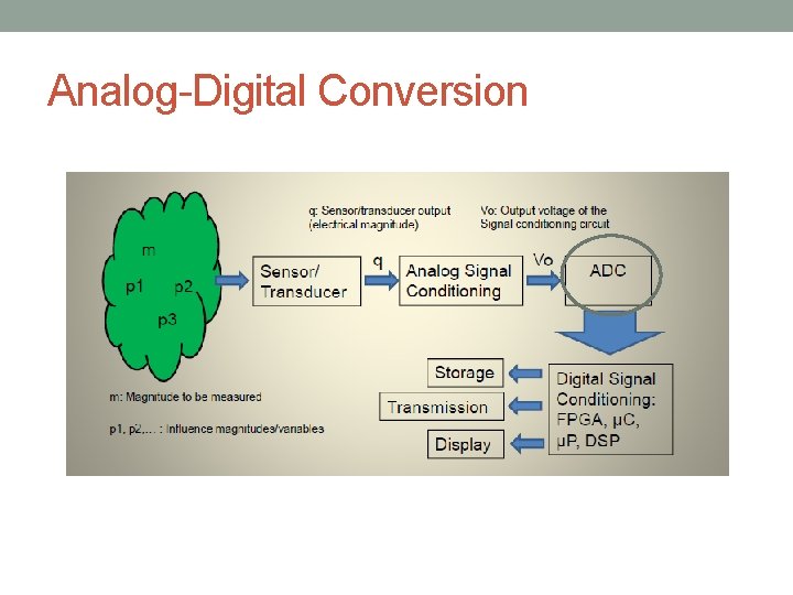
• Analog outputs from sensors and analog front- ends (analog signal conditioning) have to be converted into digital signals. • This process has two steps: • Analog signal sampling (Continuous time to discrete time) • Analog to digital conversion (Continuous voltage to discrete amplitude values)

• Analog outputs from sensors and analog front- ends (analog signal conditioning) have to be converted into digital signals. • This process has two steps: • Analog signal sampling (Continuous time to discrete time) • Analog to digital conversion (Continuous voltage to discrete amplitude values)

• To process signals digitally, they must be converted from analog to digital numbers. After a signal is processed, it is then often converted back to analog form. • Digital processing offers some clear advantages that include: • Programmability • Stability • Repeatability • Special Applications

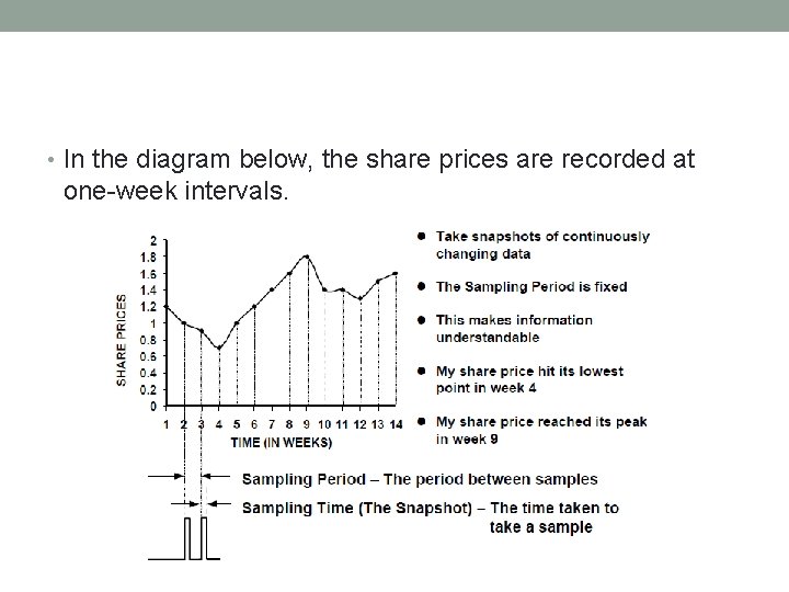
SAMPLING • To illustrate the operation of sampling, we will use the example of variations in stock market prices over a period of several weeks. • A sampling period is the time between samples. • Sampling time is ideally an instant in time when a sample is taken.

• In the diagram below, the share prices are recorded at one-week intervals.

• Must decide how often we must take the sample • This would give us a much more precise representation of the stock market fluctuations • Everyday? Every Minute? • Does the stock price changes significantly every minute?

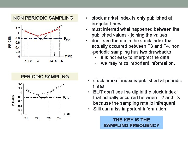
NON PERIODIC SAMPLING • stock market index is only published at irregular times • must inferred what happened between the published values - joining the values • don’t see the dip in the stock index that actually occurred between T 3 and T 4. non -periodic sampling has two drawbacks • it is not easy to interpret the data • we may miss important information. • stock market index is published at periodic times • BUT don’t see the dip in the stock index that actually occurred between T 2 and T 3 because the sampling rate is infrequent • Still can miss important information. THE KEY IS THE SAMPLING FREQUENCY

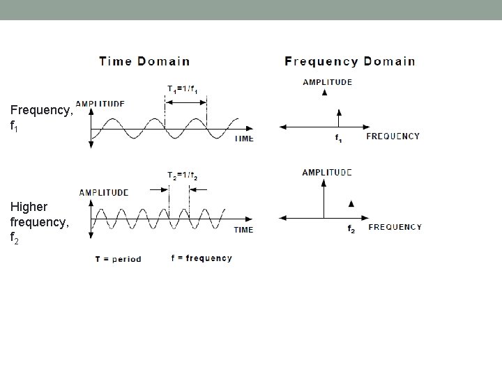
Frequency, f 1 Higher frequency, f 2

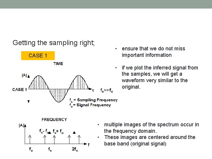
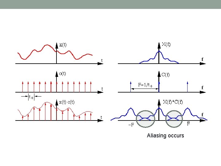
Getting the sampling right; CASE 1 • ensure that we do not miss important information • if we plot the inferred signal from the samples, we will get a waveform very similar to the original. • multiple images of the spectrum occur in the frequency domain. • These images are centered around the base band (original signal)

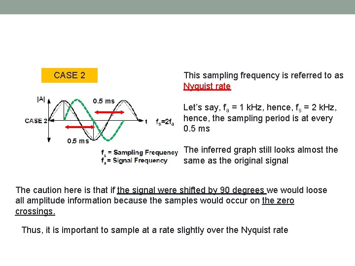
CASE 2 This sampling frequency is referred to as Nyquist rate 0. 5 ms Let’s say, fa = 1 k. Hz, hence, fs = 2 k. Hz, hence, the sampling period is at every 0. 5 ms The inferred graph still looks almost the same as the original signal The caution here is that if the signal were shifted by 90 degrees we would loose all amplitude information because the samples would occur on the zero crossings. Thus, it is important to sample at a rate slightly over the Nyquist rate

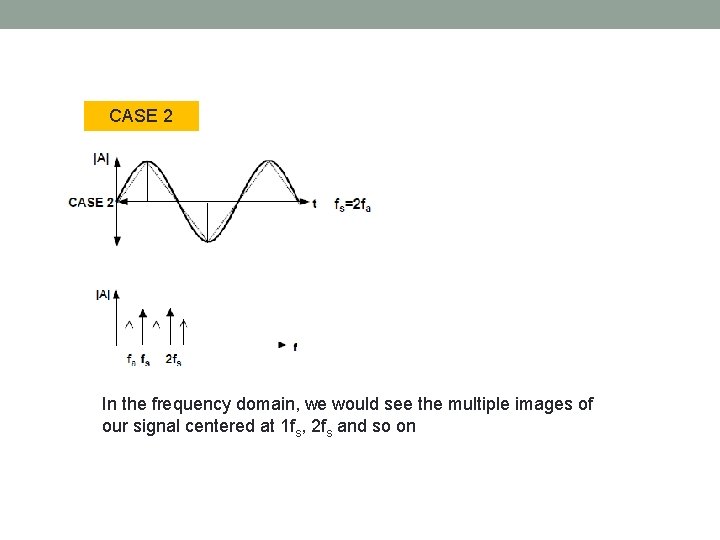
CASE 2 In the frequency domain, we would see the multiple images of our signal centered at 1 fs, 2 fs and so on

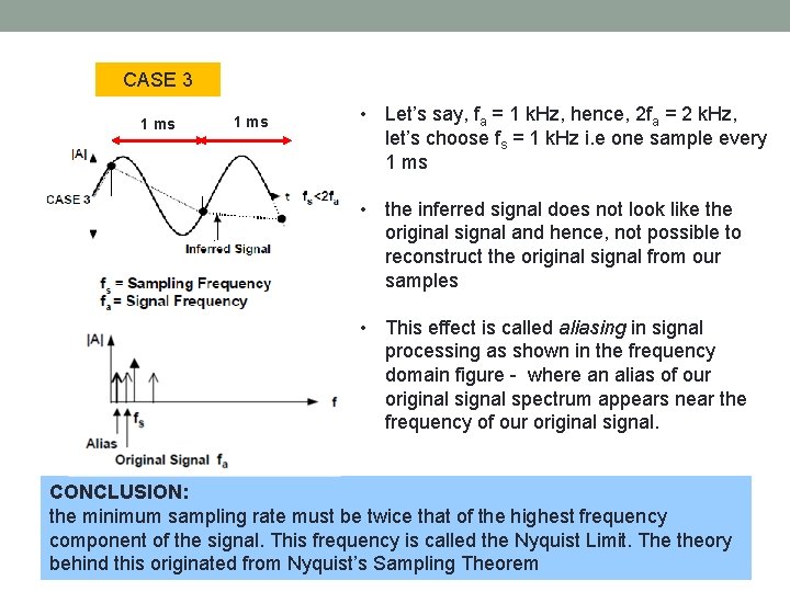
CASE 3 1 ms • Let’s say, fa = 1 k. Hz, hence, 2 fa = 2 k. Hz, let’s choose fs = 1 k. Hz i. e one sample every 1 ms • the inferred signal does not look like the original signal and hence, not possible to reconstruct the original signal from our samples • This effect is called aliasing in signal processing as shown in the frequency domain figure - where an alias of our original signal spectrum appears near the frequency of our original signal. CONCLUSION: the minimum sampling rate must be twice that of the highest frequency component of the signal. This frequency is called the Nyquist Limit. The theory behind this originated from Nyquist’s Sampling Theorem

Aliasing occurs

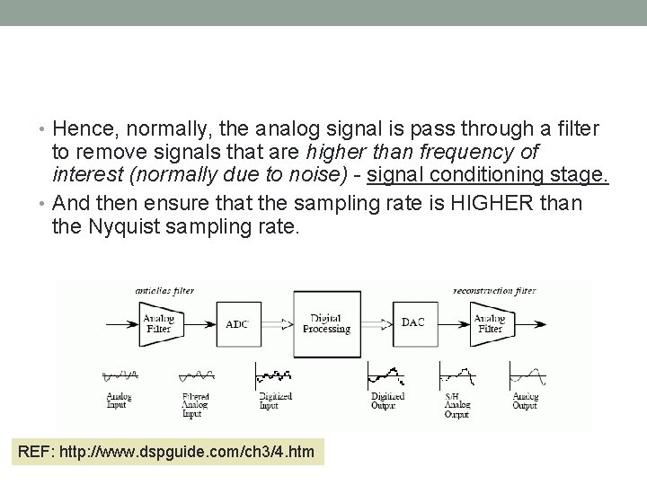
• Hence, normally, the analog signal is pass through a filter to remove signals that are higher than frequency of interest (normally due to noise) - signal conditioning stage. • And then ensure that the sampling rate is HIGHER than the Nyquist sampling rate. REF: http: //www. dspguide. com/ch 3/4. htm

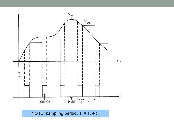
DIGITIZING AND QUANTIZATION • covered the concept of sampling a signal and filtering it with an anti-aliasing filter. • next stage is to convert the signal to a digital representation. • the basic sampling function is achieved by using a sample and hold circuit, which maintains the sampled level until the next sample is taken. • The result of this is the staircase effect

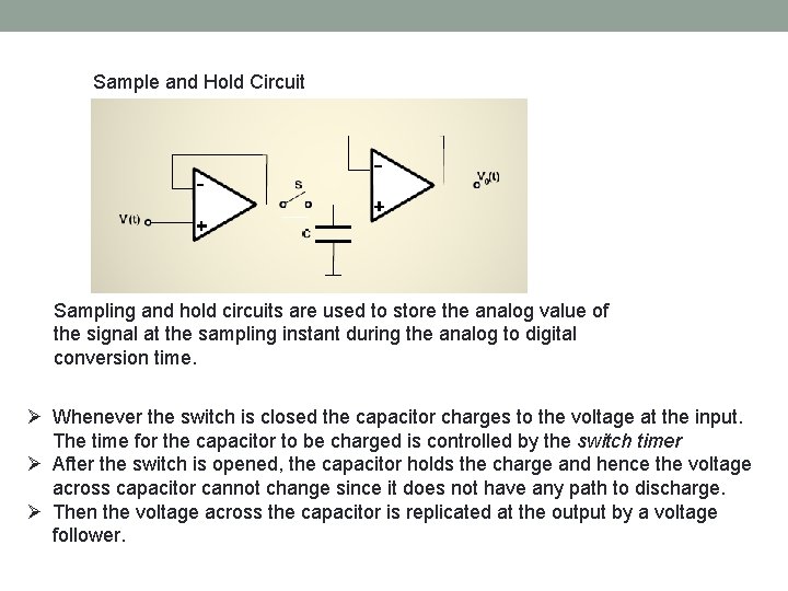
Sample and Hold Circuit Sampling and hold circuits are used to store the analog value of the signal at the sampling instant during the analog to digital conversion time. Ø Whenever the switch is closed the capacitor charges to the voltage at the input. The time for the capacitor to be charged is controlled by the switch timer Ø After the switch is opened, the capacitor holds the charge and hence the voltage across capacitor cannot change since it does not have any path to discharge. Ø Then the voltage across the capacitor is replicated at the output by a voltage follower.

vin vout NOTE: sampling period, T = ts + t. H

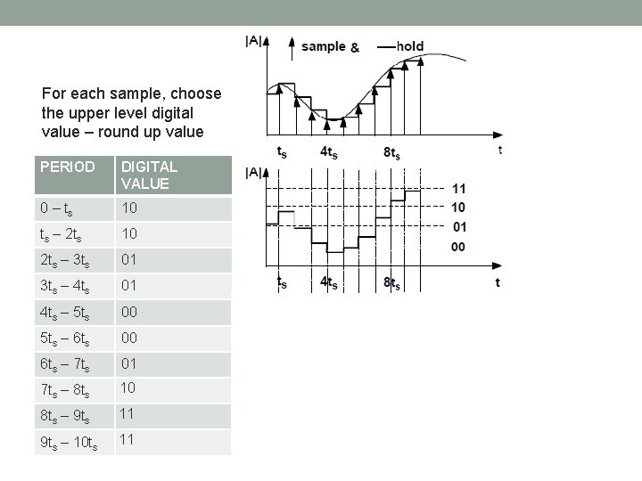
For each sample, choose the upper level digital value – round up value PERIOD DIGITAL VALUE 0 – ts 10 ts – 2 ts 10 2 ts – 3 ts 01 3 ts – 4 ts 01 4 ts – 5 ts 00 5 ts – 6 ts 00 6 ts – 7 ts 01 7 ts – 8 ts 10 8 ts – 9 ts 11 9 ts – 10 ts 11 Quantization can be thought of as classifying the signal into certain bands.

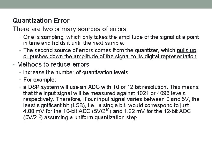
Quantization Error There are two primary sources of errors. • One is sampling, which only takes the amplitude of the signal at a point in time and holds it until the next sample. • The second source of errors comes from the quantizer, which pulls up or pushes down the amplitude of the signal to its digital representation. • Methods to reduce errors • increase the number of quantization levels • For example: • a DSP system will use an ADC with 10 or 12 bit resolution. This means that the input signal will be measured against 1024 or 4096 levels, respectively. Therefore, if our input signal varies between 0 and 5 V, the least significant bit (LSB), i. e. , a single bit, would correspond to just 4. 88 m. V for the 10 -bit ADC (5 V/210) and 1. 22 m. V for the 12 -bit ADC (5 V/212) assuming a uniform quantization step.

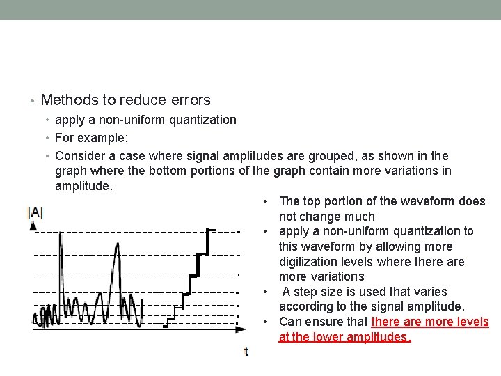
• Methods to reduce errors • apply a non-uniform quantization • For example: • Consider a case where signal amplitudes are grouped, as shown in the graph where the bottom portions of the graph contain more variations in amplitude. • The top portion of the waveform does not change much • apply a non-uniform quantization to this waveform by allowing more digitization levels where there are more variations • A step size is used that varies according to the signal amplitude. • Can ensure that there are more levels at the lower amplitudes.

• Summary: to convert an analog signal to digital, the steps are: i. iii. iv. Limit the spectrum Sample and hold Quantize each sample Obtain digital data stream • Common types of ADC • Flash ADC • Successive Approximation ADC

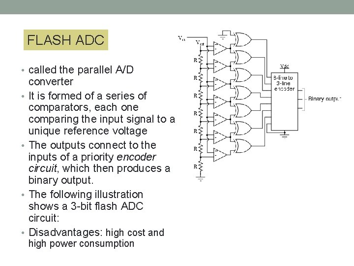
FLASH ADC • called the parallel A/D • • converter It is formed of a series of comparators, each one comparing the input signal to a unique reference voltage The outputs connect to the inputs of a priority encoder circuit, which then produces a binary output. The following illustration shows a 3 -bit flash ADC circuit: Disadvantages: high cost and high power consumption

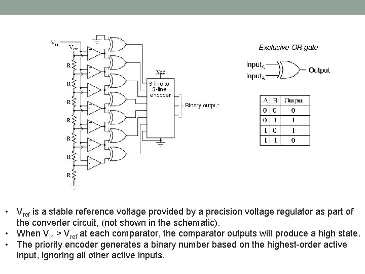
• Vref is a stable reference voltage provided by a precision voltage regulator as part of the converter circuit, (not shown in the schematic). • When Vin > Vref at each comparator, the comparator outputs will produce a high state. • The priority encoder generates a binary number based on the highest-order active input, ignoring all other active inputs.

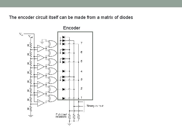
The encoder circuit itself can be made from a matrix of diodes Encoder

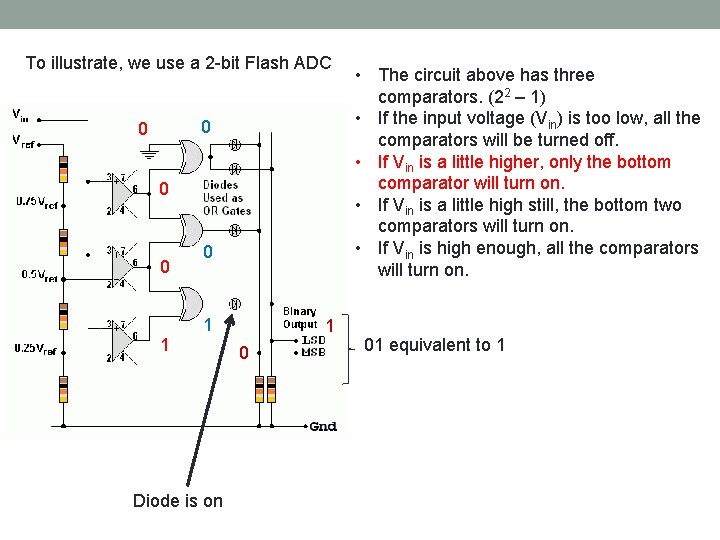
To illustrate, we use a 2 -bit Flash ADC 0 0 1 0 1 Diode is on 1 0 • The circuit above has three comparators. (22 – 1) • If the input voltage (Vin) is too low, all the comparators will be turned off. • If Vin is a little higher, only the bottom comparator will turn on. • If Vin is a little high still, the bottom two comparators will turn on. • If Vin is high enough, all the comparators will turn on. 01 equivalent to 1

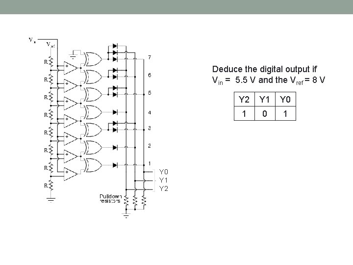
Deduce the digital output if Vin = 5. 5 V and the Vref = 8 V Y 0 Y 1 Y 2 Y 1 Y 0 1

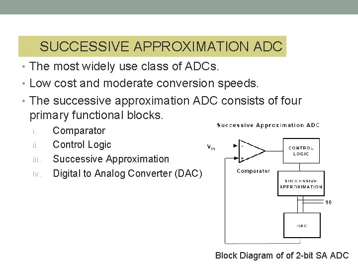
SUCCESSIVE APPROXIMATION ADC • The most widely use class of ADCs. • Low cost and moderate conversion speeds. • The successive approximation ADC consists of four primary functional blocks. i. iii. iv. Comparator Control Logic Successive Approximation Digital to Analog Converter (DAC) Block Diagram of of 2 -bit SA ADC

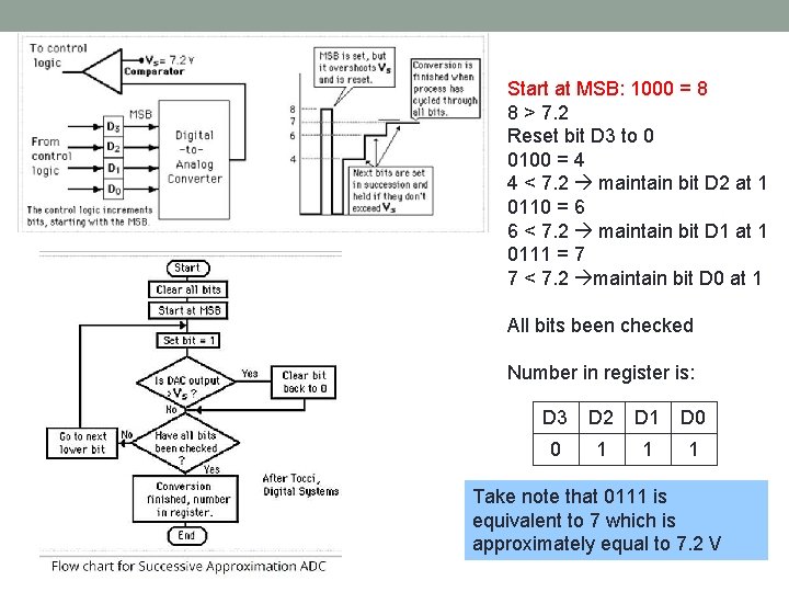
Start at MSB: 1000 = 8 8 > 7. 2 Reset bit D 3 to 0 0100 = 4 4 < 7. 2 maintain bit D 2 at 1 0110 = 6 6 < 7. 2 maintain bit D 1 at 1 0111 = 7 7 < 7. 2 maintain bit D 0 at 1 All bits been checked Number in register is: D 3 D 2 D 1 D 0 0 1 1 1 Take note that 0111 is equivalent to 7 which is approximately equal to 7. 2 V

• An N-bit SA ADC will require N comparison periods and will not be ready for the next conversion until the current one is complete. • Therefore, although, these ADCs are power- and spaceefficient, SA ADC is considered slow.