1 Instrumentation and Product Testing AnalogtoDigital Converter ADC
- Slides: 22

1 Instrumentation and Product Testing Analog-to-Digital Converter (ADC) And Digital-to-Analog Converter (DAC)

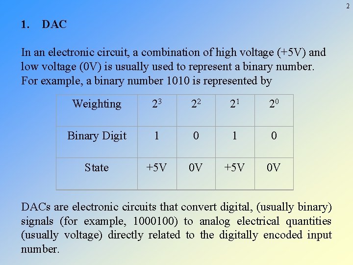
2 1. DAC In an electronic circuit, a combination of high voltage (+5 V) and low voltage (0 V) is usually used to represent a binary number. For example, a binary number 1010 is represented by Weighting 23 22 21 20 Binary Digit 1 0 State +5 V 0 V DACs are electronic circuits that convert digital, (usually binary) signals (for example, 1000100) to analog electrical quantities (usually voltage) directly related to the digitally encoded input number.

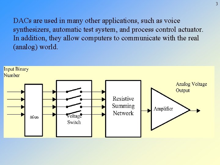
3 DACs are used in many other applications, such as voice synthesizers, automatic test system, and process control actuator. In addition, they allow computers to communicate with the real (analog) world.

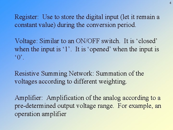
4 Register: Use to store the digital input (let it remain a constant value) during the conversion period. Voltage: Similar to an ON/OFF switch. It is ‘closed’ when the input is ‘ 1’. It is ‘opened’ when the input is ‘ 0’. Resistive Summing Network: Summation of the voltages according to different weighting. Amplifier: Amplification of the analog according to a pre-determined output voltage range. For example, an operation amplifier

5 The two most popular types of resistive summing networks are: · Weighted binary resistance type, and · Ladder resistance (R-2 R) type

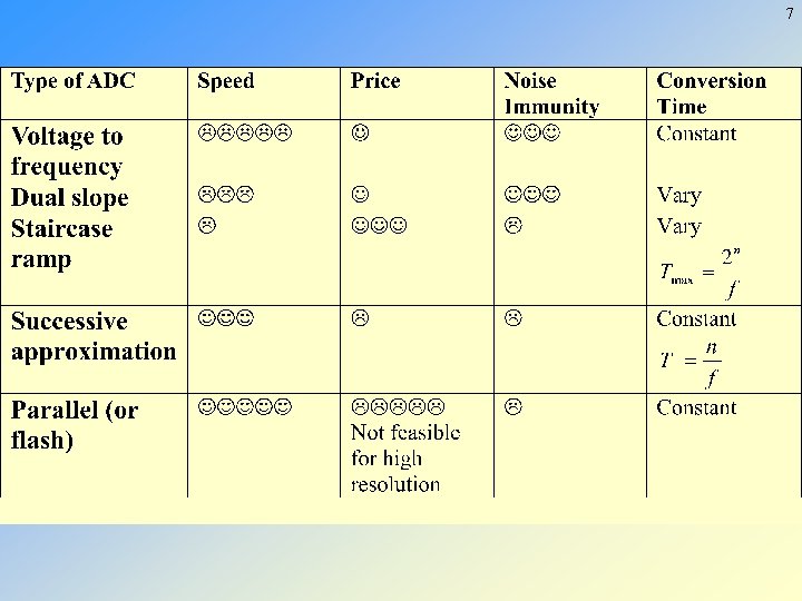
6 2. ADC Numerous methods are used for converting analog signals to digital form. Five most commonly used methods are listed below: • • • Staircase ramp Successive approximation Dual slope Voltage to frequency Parallel (or flash)

7

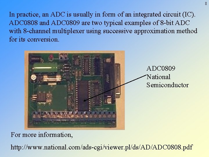
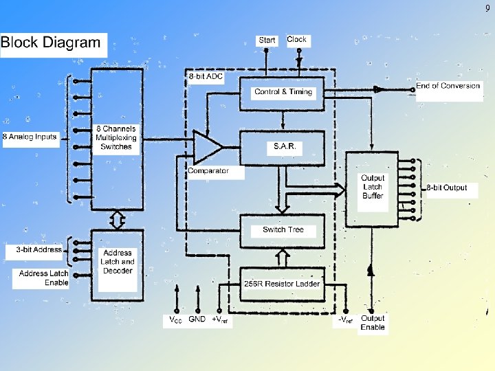
8 In practice, an ADC is usually in form of an integrated circuit (IC). ADC 0808 and ADC 0809 are two typical examples of 8 -bit ADC with 8 -channel multiplexer using successive approximation method for its conversion. ADC 0809 National Semiconductor For more information, http: //www. national. com/ads-cgi/viewer. pl/ds/AD/ADC 0808. pdf

9

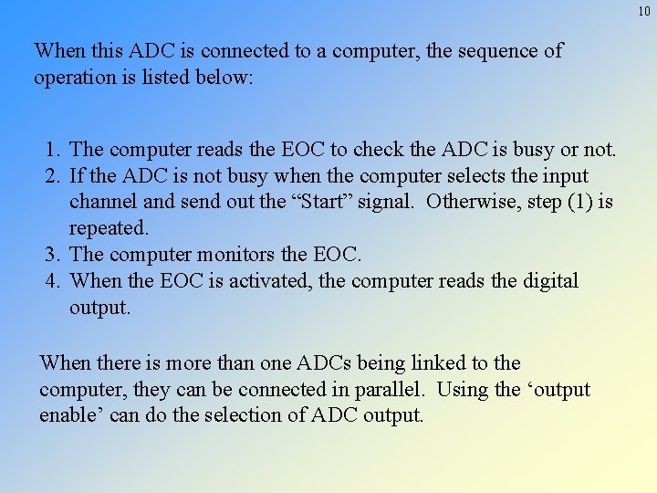
10 When this ADC is connected to a computer, the sequence of operation is listed below: 1. The computer reads the EOC to check the ADC is busy or not. 2. If the ADC is not busy when the computer selects the input channel and send out the “Start” signal. Otherwise, step (1) is repeated. 3. The computer monitors the EOC. 4. When the EOC is activated, the computer reads the digital output. When there is more than one ADCs being linked to the computer, they can be connected in parallel. Using the ‘output enable’ can do the selection of ADC output.

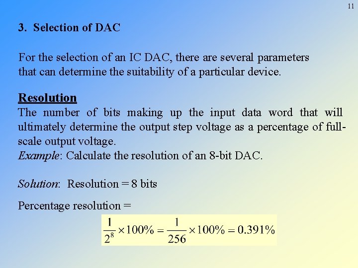
11 3. Selection of DAC For the selection of an IC DAC, there are several parameters that can determine the suitability of a particular device. Resolution The number of bits making up the input data word that will ultimately determine the output step voltage as a percentage of fullscale output voltage. Example: Calculate the resolution of an 8 -bit DAC. Solution: Resolution = 8 bits Percentage resolution =

12 Output Voltage Range This is the difference between the maximum and minimum output voltages expressed in volts. Example: Calculate the output voltage range of a 4 -bit DAC if the output voltage is +4. 5 V for an input of 0000 and +7. 5 V for an input of 1111. Solution: Output voltage range = 7. 5 – 4. 5 = 3. 0 V

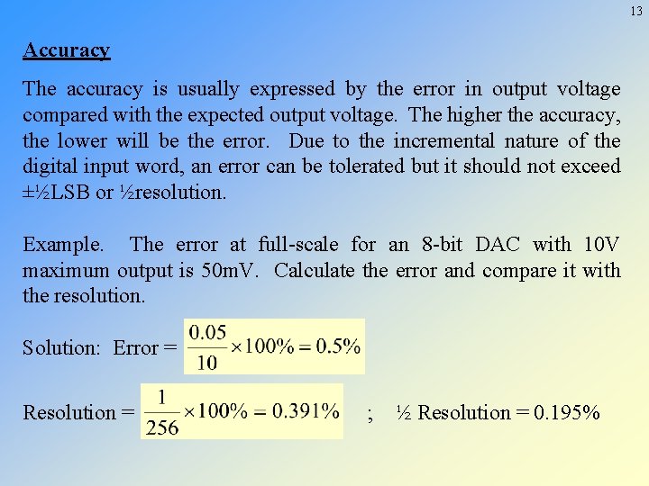
13 Accuracy The accuracy is usually expressed by the error in output voltage compared with the expected output voltage. The higher the accuracy, the lower will be the error. Due to the incremental nature of the digital input word, an error can be tolerated but it should not exceed ±½LSB or ½resolution. Example. The error at full-scale for an 8 -bit DAC with 10 V maximum output is 50 m. V. Calculate the error and compare it with the resolution. Solution: Error = Resolution = ; ½ Resolution = 0. 195%

14 The accuracy is not as good as the error = ½ resolution, but for many applications, it is quite satisfactory. Some commercially available DACs have their accuracy specified as worse than ½ resolution. Sources of errors may be broadly classified under four categories: · Non-monotonicity · Non-linearity · Scale-factor error · Offset error

15 Settling time The time taken for the applied digital input to be converted to an analog output. Typical period can be as low as 100 ns, making DA conversion a very fast process compared with those of AD conversion. Input coding The digital input can be in binary format or it can be in binary coded decimal format depending on the application. Binary format is more commonly used.

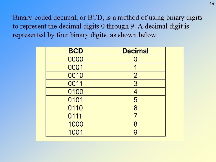
16 Binary-coded decimal, or BCD, is a method of using binary digits to represent the decimal digits 0 through 9. A decimal digit is represented by four binary digits, as shown below:

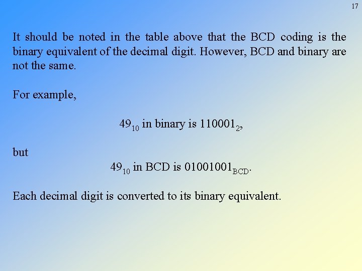
17 It should be noted in the table above that the BCD coding is the binary equivalent of the decimal digit. However, BCD and binary are not the same. For example, 4910 in binary is 1100012, but 4910 in BCD is 01001001 BCD. Each decimal digit is converted to its binary equivalent.

18 4. Selection of ADC The parameters used in selecting an ADC are very similar to those considered for a DAC selection. • Error/Accuracy: Quantising error represents the difference between an actual analog value and its digital representation. Ideally, the quantising error should not be greater than ± ½ LSB. • Resolution: DV to cause 1 bit change in output • Output Voltage Range Input Voltage Range • Output Settling Time Conversion Time • Output Coding (usually binary)

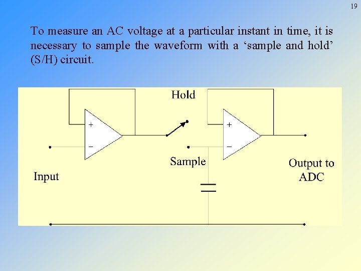
19 To measure an AC voltage at a particular instant in time, it is necessary to sample the waveform with a ‘sample and hold’ (S/H) circuit.

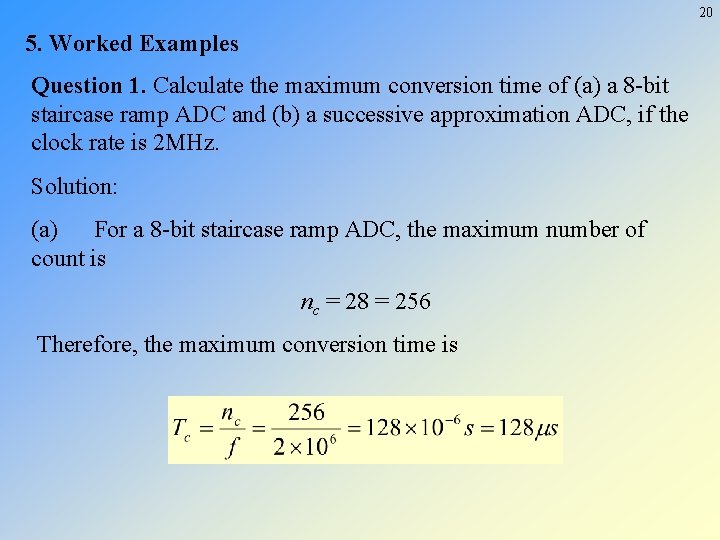
20 5. Worked Examples Question 1. Calculate the maximum conversion time of (a) a 8 -bit staircase ramp ADC and (b) a successive approximation ADC, if the clock rate is 2 MHz. Solution: (a) For a 8 -bit staircase ramp ADC, the maximum number of count is nc = 28 = 256 Therefore, the maximum conversion time is

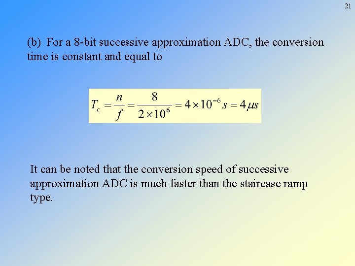
21 (b) For a 8 -bit successive approximation ADC, the conversion time is constant and equal to It can be noted that the conversion speed of successive approximation ADC is much faster than the staircase ramp type.

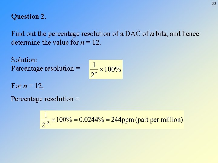
22 Question 2. Find out the percentage resolution of a DAC of n bits, and hence determine the value for n = 12. Solution: Percentage resolution = For n = 12, Percentage resolution =