Chapter 12 AnalogtoDigital Converter Basics of AD Conversion

Chapter 12 Analog-to-Digital Converter
 • Many embedded systems need to deal")
Basics of A/D Conversion (1 of 2) • Many embedded systems need to deal with nonelectric quantities: weight, humidity, pressure, weight, mass or airflow, temperature, light intensity, and speed. • These nonelectric quantities are analog in nature. • Analog quantities must be converted into digital format so that they can be processed by the computer. • An A/D converter can only deal with electric voltage.
 • Any nonelectric quantity must be converted")
Basics of A/D Conversion (2 of 2) • Any nonelectric quantity must be converted into an electric quantity using a certain type of transducer. • A transducer converts a nonelectric quantity into an electric quantity. • The output of a transducer may not be in a suitable range for A/D conversion. • A signal conditioning circuit is needed to shift and scale the transducer output to a range suitable for A/D conversion.
 • An ideal A/D converter")
Analog Voltage and Digital Code Characteristic (1 of 2) • An ideal A/D converter should have a characteristic as shown. • An A/D converter with characteristic as shown would need infinite number of bits to represent the A/D conversion result.
 • An n-bit A/D converter")
Analog Voltage and Digital Code Characteristic (2 of 2) • An n-bit A/D converter has 2 n possible output code values. • The output characteristic of an n-bit A/D ideal converter is shown. • The area above and below the dotted line is called quantization error. • Using n-bit to represent A/D conversion has an average error of 2 n+1. • A real A/D converter output may have nonlinearity and nonmonotonicity errors
 A/D conversion – 2 n comparators are used")
A/D Conversion Algorithms • Parallel (Flash) A/D conversion – 2 n comparators are used – One input to each comparator is the voltage to be converted. – The second input to each comparator is the voltage that represents one of the 2 n combinations. – The comparator output will be high if the analog input is higher than the voltage that represents one of the 2 n combinations. – The largest n-bit value that causes the comparator output to become true is selected as the A/D conversion value. – The conversion speed is very fast. – The drawback is cost. – Major applications are those that require high speed but low resolution.

Slope and Double-Slope A/D Converters • Use capacitors’ charging and discharging behavior to perform A/D conversion • Require only simple hardware and is popular in low-speed applications • Has been used in Microchip PIC 14400 family microcontrollers

Sigma-Delta A/D Converters • Use over-sampling technique to perform A/D conversion • Has good noise immunity and can achieve high resolution • Popular in high-resolution applications • Performance becomes acceptable with the advancement in CMOS technology
 • Approximates the analog signal in n steps.")
Successive Approximation Method (1 of 3) • Approximates the analog signal in n steps. • The first step initializes the SAR register to 0. • Perform a series of guessing steps that starts from the most significant bit and proceeding toward the least significant bit. • For every bit in SAR register guess it to be 1. • Converts the value of the SAR register to analog voltage. • Compares the D/A output with the analog input and clears the bit to 0 if the D/A output is larger.
")
Successive Approximation Method (2 of 3)
")
Successive Approximation Method (3 of 3)
 and")
Optimal Voltage Range for A/D Conversion • Needs a low reference voltage (VRL) and a high reference voltage (VRH) in performing A/D conversion. • VRL is often set to ground level. • VRH is often set to VDD. • Most A/D converter are ratiometric – A 0 V (or VRL) analog input is converted to the digital code of 0. – A VDD (or VRH) analog input is converted to the digital code of 2 n – 1. – A k-V input will be converted to the digital code of k (2 n – 1) VDD. • The A/D conversion result will be most accurate if the value of analog signal covers the whole voltage range from VRL to VRH. • The A/D conversion result k can be translated back to an analog voltage VK by the following equation: VK = VRL + (range k) (2 n – 1)

• Example 12. 1 Suppose that there is a 10 -bit A/D converter with VRL = 1 V and VRH = 4 V. Find the corresponding voltage values for the A/D conversion results of 25, 80, 240, 500, 720, 800, and 900. • Solution: range = VRH – VRL = 4 V – 1 V = 3 V V(25) V(80) V(240) V(500) V(720) V(800) V(900) = 1 V + (3 25) (210 – 1) = 1. 07 V = 1 V + (3 80) (210 – 1) = 1. 23 V = 1 V + (3 240) (210 – 1) = 1. 70 V = 1 V + (3 500) (210 – 1) = 2. 47 V = 1 V + (3 720) (210 – 1) = 3. 11 V = 1 V + (3 800) (210 – 1) = 3. 35 V = 1 V + (3 900) (210 – 1) = 3. 64 V

Scaling Circuit • • Some transducer has the an output voltage in the range of 0 ~ VZ, where VZ < VDD. VZ can be much smaller than VDD. When VZ is much smaller than VDD, the A/D conversion result cannot be accurate. The solution to this problem is to use an scaling circuit to amplify the transducer output to cover the whole range of 0 V VRH to VDD. AV = VOUT VIN = (R 1 + R 2) R 1 = 1 + R 2/R 1 • Example 12. 2 Choose appropriate values of R 1 and R 2 in Figure 12. 6 to scale a voltage in the range of 0~200 m. V to 0~5 V. • Solution: AV = 1 + R 2/R 1 = 5 V / 200 m. V = 25 R 2/R 1 = 24 Choose R 1 = 10 K and R 2 = 240 K to achieve the desired ratio.

Voltage Translation Circuit • Some transducer has output voltage in the range from V 1 to V 2 (V 2 > V 1). • The accuracy of the A/D conversion will be more accurate if this voltage can be scaled and shifted to 0 ~ VDD. • The circuit shown can shift and scale the voltage from V 1 to V 2 to the range of 0~VDD.

• Example 12. 3 Choose appropriate resistor values and the adjusting voltage so that the circuit shown in Figure 12. 7 c can shift the voltage from the range of – 1. 2 V ~ 3. 0 V to the range of 0 V ~ 5 V. • Solution: Applying Equation 12. 5: 0 = -1. 2 (Rf/R 1) – (Rf/R 2) V 1 5 = 3. 0 (Rf/R 1) – (Rf/R 2) V 1 - By choosing R 0 = R 1 = 10 K , R 2 = 50 K , Rf = 12 KW, and V 1 = -5 V, one can translate and scale the voltage to the desired range.

The HCS 12 A/D Converter • A HCS 12 member may have one or two 8 -channel 10 -bit A/D converters. • The highest conversion clock is 2 MHz. • At 2 MHz conversion clock, a sample may take 6 ms or 7 ms to complete a conversion for 8 -bit and 10 -bit resolution. • An A/D conversion can be started by writing into a control register or by an external trigger input. • The successive approximation method is used to perform the conversion. • The conversion result can be right-justified unsigned, leftjustified signed, and left-justified unsigned.

Signal Pins Related to A/D Converter • The AD 0 module has analog input pins AN 0 ~ AN 7. • The AD 1 module has analog input pins AN 8 ~ AN 15. • The AN 7 pin can be optionally used as the trigger input pin for AD 0 module. • The AN 15 pin can be optionally used as the trigger input pin for AD 1 module. • VRH and VRL are the high and low reference voltage input. • VDDA and VSSA are power supply and ground inputs for the A/D converters.

Registers Related to A/D Converters • Each A/D module has the following registers: – Six control registers: ATDx. CTL 0 ~ ATDx. CTL 5. (ATDx. CTL 0 and ATDx. CTL 1 are used for factory testing only). – Two status registers: ATDx. STAT 0 and ATDx. STAT 1 – Two testing registers: ATDx. TEST 0 and ATDx. TEST 1 – One input enable register: ATDx. DIEN – One port data register: PTADx – Eight 16 -bit result registers ATDx. DR 0~ATDx. DR 7 – where, x = 0 or 1
")
ATD Control Register 2 (ATD 0 CTL 2, ATD 1 CTL 2)

A/D External Triggering • A/D external triggering can be edge-triggering or level-triggering. • The choice of external triggering is controlled by the ATDx. CTL 2 register.
 (1")
ATD Control Register 3 (ATD 0 CTL 3 and ATD 1 CTL 3) (1 of 2) • This register sets the conversion sequence length, enables/disables the FIFO mode for result registers, and controls the ATD behavior in freeze mode (BDM mode). • If the FIFO bit is 0, the result of the first conversion appears in the first result register, the second conversion appears in the second result register, and so on. • If the FIFO bit is 1, then the result of the first conversion appears in the result register specified by the conversion counter.
 (2")
ATD Control Register 3 (ATD 0 CTL 3 and ATD 1 CTL 3) (2 of 2)
 (1")
ATD Control Register 4 (ATD 0 CTL 4 and ATD 1 CTL 4) (1 of 2) • This register sets the conversion clock frequency, the length of the second phase of the sample time, and the resolution of the A/D conversion. • Writes to this register will abort the current conversion. • There are two stages in the sample time. The first stage sample time is fixed at two conversion clock period. The second stage is selected by SMP 1 and SMP 2 bits of this register.
 (2")
ATD Control Register 4 (ATD 0 CTL 4 and ATD 1 CTL 4) (2 of 2)
 • • • Selects the type of")
ATD Control Register 5 (1 of 3) • • • Selects the type of conversion sequence and the analog input channels to be sampled. Writes to this register will abort the current conversion. Table 12. 4 selects the channel to be converted. Table 12. 5 summarizes the result data formats available and how they are set up using the control bits. Table 12. 6 illustrates the difference between the signed and unsigned, left justified and right justified output codes for an input signal range between 0 and 5. 12 V.
")
ATD Control Register 5 (2 of 3)
")
ATD Control Register 5 (3 of 3)
 • Each")
ATD Status Register (ATD 0 STAT 0 and ATD 1 STAT 0) • Each status flag can be cleared by writing a 1 to it.
 • The")
ATD Test Register 1 (ATD 0 TEST 1, ATD 1 TEST 1) • The SC bit is used to enable special channel conversion.
 • A")
ATD Status Register 1 (ATD 0 STAT 1, ATD 1 STAT 1) • A flag can be cleared by one of the following: – Write to ATDx. CTL 5 register. – If AFFC = 0 and read of ATDx. STAT 1 followed by read of result register ATDx. DRy. – If AFFC = 1 and read of result register ATDx. DRy
 • This register allows")
ATD Input Enable Register (ATD 0 DIEN, ATD 1 DIEN) • This register allows the user to enable a Port ADx pin as a digital input.
 • The port pins are shared with")
Port Data Register (PTAD 0, PTAD 1) • The port pins are shared with analog inputs AN 0~AN 7 and AN 8~AN 15.
 • Each result")
ATD Conversion Result Registers (ATDx. DRy, x = 0~1, y= 0~7) • Each result register is 16 -bit and can be further divided into two 8 -bit registers ATDx. DRHy and ATDx. DRLy. • The A/D conversion result can be stored rightjustified or left-justified.

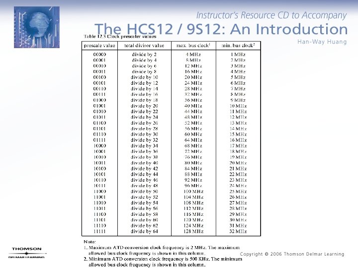
ATD Module Clock • The frequency range of the A/D converter clock is from 500 KHz to 2 MHz. • The user sets a prescaler to the bus clock to derive the ATD clock signal.

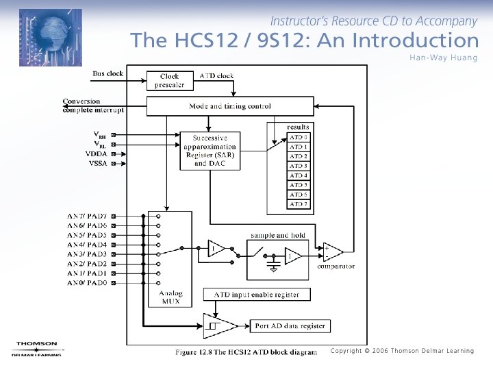
Sample and Hold Stage • As shown in Figure 12. 8, a sample and hold stage accepts analog signals from the input multiplexer and stores them as charge on the sample capacitor. • The sampling process has two stages. • The first stage of the sampling process takes two A/D clock cycles to charge the sample capacitor. • The second stage of the sampling process stores the charge in the storage node for a programmable 2, 4, 8, or 16 cycles. • The conversion time of a sample is given by the following equation:

The A/D Conversion Time • The A/D conversion time is the sum of the converter time and the sample time. • The conversion timings for 500 KHz and 2 MHz are shown in Table 12. 8.

Input Channel Wrap Around • In the case of a multiple channel conversion sequence, when input selector goes past channel AN 7, it wraps around to channel AN 0.

• Example 12. 4 Assuming that S 8 C~S 1 C (ATD 0 CTL 3) are set to 0101 and CC~CA (ATD 0 CTL 5) are set to 110, what is the conversion sequence for this setting? • Solution: – The first channel to be converted is AN 6. – There are five channels to be converted. – The conversion sequence is as follows: AN 6, AN 7, AN 0, AN 1, and AN 2.

FIFO Mode • All eight 16 -bit result registers are organized into a circular ring. • The conversion counter in the ATDx. STAT 0 register specifies the result register to hold the current conversion result. • In the FIFO mode, the conversion is not reset to 0 when a new conversion sequence is started. • In the FIFO mode, the first conversion result may not be stored in ATDx. DR 0.

• Example 12. 5 Assume that the following setting was programmed before a new conversion is started: – – The conversion counter value in the ATD 0 STAT 0 register is 5. The channel select code of the ATD 0 CTL 5 register is 6. The conversion sequence limit of the ATD 0 CTL 3 register is set to 5. The MULT bit of the ATD 0 CTL 5 register is set to 1. • How would the conversion results be stored when the FIFO mode is selected or not selected? • Solution: – The conversion counter specifies the result register to hold the first conversion result. – The channel select code specifies the first channel to be converted. – The conversion sequence limit specifies the number of channels to be converted.

Procedure for Performing A/D Conversion • Step 1 – – – • • Connect the hardware properly: VDDA: connect to VDD (5 V). VSSA: connect to GND VRH: connect to VDD (5 V) VRL: connect to GND Step 2 – If the transducer is not in the appropriate range, use a signal conditioning circuit to shift and scale it to between VRL and VRH. Step 3 – Select the appropriate channel (s) and operation modes by programming the ATD control register 5. Writing to the ATDx. CTL 5 register starts an A/D conversion sequence. • Step 4 – Wait until the SCF flag of the status register ATDx. STAT 0 is set, then collect the A/D conversion results and store them in memory.

• Example 12. 6 Write a subroutine to initialize the AD 0 converter for the MC 9 S 12 DP 256 and start the conversion with the following setting: – – – • Nonscan mode Select channel 7 (single channel mode) Fast ATD flag clear all Stop AD 0 in wait mode Disable interrupt Perform four conversions in a sequence Disable FIFO mode Finish current conversion then freeze when BDM becomes active 10 -bit operation and 2 A/D clock periods of the second stage sample time Choose 2 MHz as the conversion frequency for the 24 MHz bus clock Result is unsigned and right justified Solution: – The setting of ATD 0 CTL 2 • • • Enable AD 0 Select fast flag clear all (set bit 6 to 1) Stop AD 0 when in wait mode (set bit 5 to 1) Disable external trigger on channel 7 (set bits 4, 3, and 2 to 0) Disable AD 0 interrupt (set bit 1 to 0) Write the value 0 x. E 0 to ATD 0 CTL 2.

– The setting of ATD 0 CTL 3: • Perform four conversions • Disable FIFO mode • When BDM becomes active, complete the current conversion then freeze • Write the value of 0 x 22 into this control register. – The setting of ATD 0 CTL 4: • • Select 10 -bit operation (set bit 7 to 0) Two A/D clock periods for sample time (set bits 6 and 5 to 00) Set the value of PRS 4~PRS 0 to 00101 Write the value 0 x 05 to this control register. – The setting of ATD 0 CTL 5: • • • Result register right justified (set bit 7 to 1) Result is unsigned (set bit 6 to 0) Nonscan mode (set bit 5 to 0) Single channel mode (set bit 4 to 0) Select channel 7 (set bits 2. . 0 to 111) Write the value 0 x 87 to this control register

The Assembly Subroutine that Performs the AD 0 Initialization #include "c: miniidehcs 12. inc" open. ATD 0 movb #$E 0, ATD 0 CTL 2 ldy #2 jsr delayby 10 us ; wait for 20 us movb #$22, ATD 0 CTL 3 movb #$05, ATD 0 CTL 4 rts #include “c: miniidedelay. asm”

The C Function that Performs the AD 0 Initialization #include “c: egnu 091includedelay. c” void open. AD 0 (void) { ATD 0 CTL 2 = 0 x. E 0; delayby 10 us(2); ATD 0 CTL 3 = 0 x 22; ATD 0 CTL 4 = 0 x 05; }

• Example 10. 7 Write a program to perform A/D conversion on the analog signal connected to the AN 7 pin. Collect 20 A/D conversion results and store them at memory locations starting from $1000. Use the same configuration as in Example 10. 6. • Solution: - Example 10. 6 configures AD 0 to perform 4 conversions in a sequence on channel AN 7. - Need to write into the ATD 0 CTL 5 five times to collect twenty samples. #include "c: miniidehc 12. inc" org $1500 lds #$1500 ldx #$1000 ; use index register X as a pointer to the buffer jsr open. AD 0 ; initialize the ATD 0 converter ldy #5 loop 5 movb #$87, ATD 0 CTL 5 ; start an A/D conversion sequence brclr ATD 0 STAT 0, SCF, * movw ATD 0 DR 0, 2, x+ ; collect and save the conversion results movw ATD 0 DR 1, 2, x+ ; post-increment the pointer by 2 movw ATD 0 DR 2, 2, x+ ; “ movw ATD 0 DR 3, 2, x+ ; “ dbne y, loop 5 swi ; include the “open. AD 0 subroutine here end

C Program to Collect 20 Samples from Channel AN 7 #include “c: egnu 091includehcs 12. h” void open. AD 0 (void); int buf[20]; void main (void) { int i; open. AD 0(); for (i = 0; i < 5; i++) { ATD 0 CTL 5 = 0 x 87; /* start an A/D conversion */ while (!(ATD 0 STAT 0 & SCF)); /* Has A/D conversion completed? */ buf[4*i + 0] = ATD 0 DR 0; /* save results right justified */ buf[4*i + 1] = ATD 0 DR 1; buf[4*i + 2] = ATD 0 DR 2; buf[4*i + 3] = ATD 0 DR 3; } asm ("swi"); }

• Example 12. 8 Write a C program to be run on the Dragon 12 (or SSE 256) demo board to display the voltage (output of a potentiometer) connected to the AN 7 pin. Configure the AD 0 properly and perform 5 conversions per second and display the voltage on the LCD. • Solution: - The conversion result 1023 corresponds to 5 V. - Divide 204. 6 into the conversion result to convert the result back to voltage. - Multiply the conversion result by 10 and then divide the product by 2046 to get the voltage. #include “c: egnu 091includehcs 12. h” #include “c: egnu 091includedelay. c” #include “c: egnu 091includelcd_util_dragon 12. c” void open. AD 0(void); void wait 20 us (void); main(void) { char buffer[6]; /* used to hold the voltage value */ int temp; char *msg 1 = "Voltage = "; openlcd(); buffer[1] = '. '; /* decimal point */ buffer[3] = 0 x 20; /* space character */ buffer[4] = 'V'; /* volt character */ buffer[5] = 0; /* null character */
; while(1) { ATD 0 CTL 5 = 0 x 87; /*")
open. AD 0(); while(1) { ATD 0 CTL 5 = 0 x 87; /* convert AN 7, result right justified */ while(!(ATD 0 STAT 0 & SCF)); /* wait for conversion to complete */ buffer[0] = 0 x 30 + (ATD 0 DR 0 * 10 )/2046; temp = (ATD 0 DR 0 * 10)%2046; /* find the remainder */ buffer[2] = 0 x 30 + (temp * 10)/2044; /* compute the fractional digit */ cmd 2 lcd(0 x 80); /* set LCD cursor to upper left corner*/ puts 2 lcd(msg 1); /* output the message "voltage =" */ puts 2 lcd(&buffer[0]); /* output voltage string */ delayby 100 ms(2); /* wait for 200 ms */ } return 0; } void open. AD 0 (void) { int i; ATD 0 CTL 2 = 0 x. E 0; delayby 10 us(2); ATD 0 CTL 3 = 0 x 0 A; ATD 0 CTL 4 = 0 x 25; } /* enable AD 0, fast ATD flag clear, disable AD 0 in wait mode */ /* perform one conversion */ /* 4 cycles sample time, prescaler set to 12 */

Temperature Sensor TC 1047 A • It has three pins with voltage output directly proportional to the ambient temperature. • It can measure temperature in the range of -40ºC to 125ºC with a supply from 2. 7~5. 5 V. • Voltage output at -40ºC, 25ºC, and 125ºC are 100 m. V, 500 m. V, 750 m. V, 1. 75 V.

Circuit Connection Between the TC 1047 A and the HCS 12 • Example 12. 9 Convert the temperature and display it in three integral and one fractional digits using the LCD. Display the temperature in the whole range of the TC 1047 A. Update the display five times a second. E clock is 24 MHz. • Solution: - The whole temperature range is 165 o. C. - To translate from the A/D conversion result back to temperature, divide the result by 6. 2, which can be done by multiplying the result by 10 and then divide the product by 62.

#include "c: mini. IDEhcs 12. inc" period equ $2 E degree equ 223 org $1000 quo ds. b 1 rem ds. b 1 sign ds. b 1 fract ds. b 1 buf ds. b 8 org $1500 lds #$1500 ldy #2 jsr delayby 100 ms jsr openlcd ldaa #$80 jsr cmd 2 lcd ldx #msg 1 jsr puts 2 lcd jsr open. AD 0 forever movb #$20, buf+1 movb #$30, buf+2 ; ASCII code of period character ; ASCII code of degree character ; to hold string to be output to LCD ; set up stack pointer ; wait for LCD to complete ; internal configuration ; configure LCD ; set LCD cursor to upper ; left corner ; output "Temperature = " ; configure ATD 0 module ; initialize the buffer contents to 0. 0 o. C ; "

movb movb brclr ldd ldy emul ldx ediv stab tfr subb bhs negb stab movb #period, buf+3 #$30, buf+4 #degree, buf+5 #$43, buf+6 #0, buf+7 #$87, ATD 0 CTL 5 #0, sign #$30, fract ATD 0 STAT 0, SCF, * ATD 0 DR 0 #10 #62 rem y, d #40 save_quo #1, sign ; " ; degree character ; letter 'C' ; null character ; start an ATD conversion sequence ; initialize sign to positive ; initialize fractional digit to 0 ; wait for the conversion to complete ; read a conversion result ; compute result x 10 / 62 ; " ; " ; save the remainder ; transfer quotient to B ; subtract temperature offset ; if non-negative, don't touch remainder ; compute 2's complement of quotient ; temperature is negative

ldab beq ldab subb stab bra save_quo stab cal_fract ldab beq ldaa mul ldx idiv cmpb blt inx cpx bne inc bra no_round tfr addb stab rem convert #62 rem cal_fract quo rem convert #10 #62 #31 no_round #10 no_round quo convert x, d #$30 fract ; if remainder is 0, skip a few instruction ; ; compute 62 - rem ; " ; save updated quotient ; come here when positive ; compute fractional digit ; " ; " ; round off fractional digit ; " ; " ; " ; prepare to separate integer digits ; convert fractional digit to ASCII code ; "

convert add_fra ldab clra ldx idiv addb stab tfr tstb beq movb ldaa beq movb quo #10 #$30 buf+2 x, d add_fra #10 #$30 buf+1 x, d add_fra #$31, buf fract, buf+4 sign out_it #$2 D, buf ; " ; use repeated divide by 10 to separate ; integral digits ; " ; save the one's digit ; transfer quotient to D ; is quo zero? ; if integral part is 0, then add fraction digit ; separate the ten's digit ; convert and store the ten's digit ; " ; test hundred's digit ; is quotient 0? ; hundreds digit, if any, is 1 only ; insert fraction digit ; check the sign ; when minus, add minus character

out_it ldaa #$C 0 ; set cursor to 2 nd row jsr cmd 2 lcd ; " ldx #spaces ; clear the 2 nd row of the LCD jsr puts 2 lcd ; " ldaa #$C 5 ; set LCD cursor position jsr cmd 2 lcd ; " ldx #buf ; output the temperature string jsr puts 2 lcd ; " ldy #2 ; wait for 200 ms jsr delayby 100 ms ; " jmp forever ; continue ; ********************************************** ; The following function perform the AD 0 configuration. ; ********************************************** open. AD 0 movb #$E 0, ATD 0 CTL 2 ; enable AD 0, fast ATD flag clear, stop in wait mode ldy #2 jsr delayby 10 us ; wait until AD 0 is stabilized movb #$0 A, ATD 0 CTL 3 ; perform one A/D conversion movb #$25, ATD 0 CTL 4 ; 4 cycles sample time, set prescaler to 12 rts

#include "C: mini. IDElcd_util_dragon 12. asm" #include "c: mini. IDEdelay. asm" msg 1 fcc "Temperature = " dc. b 0 spaces fcc " " dc. b 0 end

C Program for Temperature Measurement #include “c: egnu 091includehcs 12. h” #include “c: egnu 091includedelay. c” #include “c: egnu 091includeconvert. c” #include “c: egnu 091includelcd_util_dragon 12. c” void open. AD 0(void); char buf[8]; char *msg 1 = "temperature = "; char *blanks = " "; void main (void) { int temp 1, temp 2; char sign, fdigit, frem; char *ptr; delayby 100 ms(2); /* wait for LCD kit to initialize */ openlcd(); /* configure LCD kit */ open. AD 0(); /* configure AD 0 module */ cmd 2 lcd(0 x 80); /* set cursor to upper left corner */ puts 2 lcd(msg 1); /* output the message "temperature = " */
 { sign = 0; /* initialize sign to be positive */ ATD 0")
while(1) { sign = 0; /* initialize sign to be positive */ ATD 0 CTL 5 = 0 x 87; /* start a conversion with result right justified */ while(!(ATD 0 STAT 0 & SCF)); /* wait until conversion is done */ temp 1 = (ATD 0 DR 0 * 10) / 62; /* integer part of temperature */ temp 2 = (ATD 0 DR 0 * 10) % 62; /* remainder part */ temp 1 -= 40; /* subtract the offset from the actual temperature */ if (temp 1 < 0){ /* temperature is negative */ sign = 1; temp 1 = ~temp 1 + 1; /* find the magnitude of temperature */ if (temp 2) { /* remainder not zero */ temp 1 --; temp 2 = 62 - temp 2; } } fdigit = (temp 2 * 10) / 62; /* compute the fractional digit */ frem = (temp 2 * 10)%62; if (frem > 31) { fdigit ++; if (fdigit == 10) { /* round off the fraction digit */ fdigit = 0; temp 1++; }
![} if (sign) { ptr = &buf[1]; buf[0] = 0 x 2 D; }](http://slidetodoc.com/presentation_image/6d6c64eaa23a97701b915082d10266d7/image-63.jpg "} if (sign) { ptr = &buf[1]; buf[0] = 0 x 2 D; }")
} if (sign) { ptr = &buf[1]; buf[0] = 0 x 2 D; } else ptr = &buf[0]; int 2 alpha(temp 1, ptr); ptr = &buf[0]; while(*ptr) ptr++; *ptr++ = '. '; *ptr++ = fdigit + 0 x 30; *ptr++ = 223; *ptr++ = 'C'; *ptr = 0; cmd 2 lcd(0 x. C 0); puts 2 lcd(blanks); cmd 2 lcd(0 x. C 5); puts 2 lcd(&buf[0]); delayby 100 ms(2); } } /* point to the first space to hold ASCII string */ /* store minus sign as the first character */ /* convert the integer part to ASCII string */ /* find the end of the integer string */ /* add a degree character */ /* temperature in Celsius */ /* terminate the temperature string */ /* move cursor to 2 nd row */ /* clear the 2 nd row */ /* set cursor to column 5 row 2 */ /* output the temperature */ /* wait for 0. 2 seconds */

The Humidity Sensor IH-3606 • • Provides a linear voltage output from 0. 8 to 3. 9 V in the full range of relative humidity 0% to 100% with 5 V power supply Is light sensitive and should be shielded from light for best result Can resist contaminant vapors, such as organic solvents, chlorine, and ammonia Requires a 1 KHz low-pass filter at its voltage output before it can be converted

Circuit Connection Between the IH-3605 and the HCS 12 • The low pass filter is implemented by a 1 K resistor and a 0. 16 m. F capacitor.

• Example 12. 10 Construct a humidity measurement system that consists of the HCS 12, an IH-3605 humidity sensor, and an LCD. The bus clock frequency of the HCS 12 is 24 MHz. • Solution: - To translate from the A/D conversion result back to humidity, divide the conversion result by 10. 23. - The same operation can be implemented by multiplying the conversion result by 100 and dividing by 1023. #include “c: egnu 091includehcs 12. h” #include “c: egnu 091includedelay. c” #include “c: egnu 091includeconvert. c” #include “c: egnu 091includelcd_util_dragon 12. c” void open. AD 0(void); char buf[10]; char *msg 1 = "humidity = "; char *blanks = " "; void main (void) { unsigned int quo, rem, frem; long temp; char *ptr, fdigit;
; /* wait for LCD kit to self initialize */ openlcd(); /*")
delayby 100 ms(2); /* wait for LCD kit to self initialize */ openlcd(); /* configure LCD kit */ open. AD 0(); /* configure AD 0 module */ cmd 2 lcd(0 x 80); /* set cursor to upper left corner */ puts 2 lcd(msg 1); /* output the message "humidity = " */ while(1) { ATD 0 CTL 5 = 0 x 87; /* start a conversion with result right justified */ while(!(ATD 0 STAT 0&SCF)); /* wait until conversion is done */ temp = (long)ATD 0 DR 0 * 100; /* force compiler to use 32 -bit to represent the product */ quo = temp / 1023; /* integer part of temperature */ rem = temp % 1023; /* remainder part */ if (quo == 100) rem = 0; /* force highest humidity to 100% only */ fdigit = (rem * 10) / 1023; /* compute the fractional digit */ frem = (rem * 10) % 1023; if (frem > 511) fdigit ++; if (fdigit == 10) { /* round off the fraction digit */ fdigit = 0; quo ++; }
![ptr = &buf[0]; int 2 alpha(quo, ptr); ptr = &buf[0]; while(*ptr) ptr++; *ptr++ =](http://slidetodoc.com/presentation_image/6d6c64eaa23a97701b915082d10266d7/image-68.jpg "ptr = &buf[0]; int 2 alpha(quo, ptr); ptr = &buf[0]; while(*ptr) ptr++; *ptr++ =")
ptr = &buf[0]; int 2 alpha(quo, ptr); ptr = &buf[0]; while(*ptr) ptr++; *ptr++ = '. '; *ptr++ = fdigit + 0 x 30; *ptr++ = '%'; *ptr = 0; cmd 2 lcd(0 x. C 0); puts 2 lcd(blanks); cmd 2 lcd(0 x. C 5); puts 2 lcd(&buf[0]); delayby 100 ms(2); /* convert the integer part to ASCII string */ /* find the end of the integer string */ /* decimal point */ /* fractional digit */ /* terminate the humidity string */ /* move cursor to 2 nd row */ /* clear the 2 nd row */ /* set cursor to column 5 row 2 */ /* output the humidity */ /* wait for 0. 2 seconds */ } } void open. AD 0(void) { ATD 0 CTL 2 = 0 x. E 0; ATD 0 CTL 3 = 0 x 0 A; ATD 0 CTL 4 = 0 x 25; delayby 10 us(2); } /* enable AD 0, fast ATD flag clear, power-down on wait */ /* perform one ATD conversion */ /* prescaler set to 12, select 4 cycles sample time */

Measuring the Barometric Pressure • • • Barometric pressure is the air pressure existing at any point within earth’s atmosphere. This pressure can be measured as an absolute pressure (with reference to absolute vacuum) or can be referenced to some other value or scale. Absolute pressure is used in meteorology and aviation. Atmosphere pressure is exponentially related to altitude. Once the pressure at a certain point is measured, the pressure at any other point can be computed. Barometric pressure can be measured in four different units.

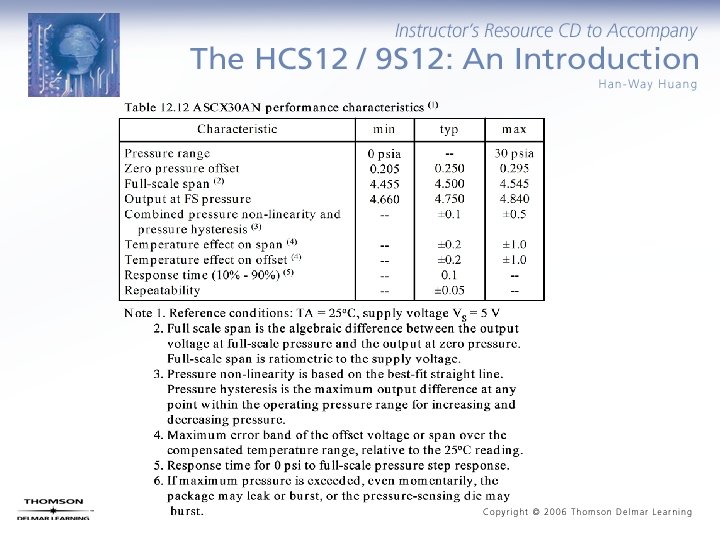
The Sen. Sym ASCX 30 AN Pressure Sensor • It is a 0 to 30 psia (psi absolute) pressure transducer. • The range of barometric pressure is between 28 to 32 inches mercury (in-Hg) or 13. 75 to 15. 72 psia or 948 to 1083. 8 mbar. • The transducer output is about 0. 15 V/psi, which would translate to 2. 06 V to 2. 36 V.

The Circuit Connection between the ASCX 30 AN and the HCS 12 • Example 12. 11 Write a program to measure and display the barometric pressure in units of mbar using the ASCX 30 AN pressure transducer. • Solution: - The offset adjustment can be achieved by using a potentiometer. - The whole barometric pressure range is 135. 8 mbar (= 1083. 8 – 948). - To translate back to barometric pressure, divide 7. 53 into the A/D conversion result or multiply the conversion result by 100 and then divide the product by 753 and then add 948 to the quotient.

#include “c: egnu 091includehcs 12. h” #include “c: egnu 091includedelay. c” #include “c: egnu 091includeconvert. c” #include “c: egnu 091includelcd_util_dragon 12. c” void open. AD 0(void); char buf[12]; char *msg 1 = "pressure = "; char *blanks = " "; void main (void) { unsigned int quo, rem, frem; long temp; char *ptr, fdigit; delayby 100 ms(2); /* wait for LCD kit to self initialize */ openlcd(); /* configure LCD kit */ open. AD 0(); /* configure AD 0 module */ cmd 2 lcd(0 x 80); /* set cursor to upper left corner */ puts 2 lcd(msg 1); /* output the message "pressure = " */ while(1) { ATD 0 CTL 5 = 0 x 87; /* start a conversion with result right justified */ while(!(ATD 0 STAT 0&SCF)); /* wait until conversion is done */
ATD 0 DR 0 * 100; quo = temp/753; /* integer part")
temp = (long)ATD 0 DR 0 * 100; quo = temp/753; /* integer part of pressure */ rem = temp%753; /* remainder part */ fdigit = (rem * 10)/753; /* compute the fractional digit */ frem = (rem * 10) % 753; if (frem > 377) fdigit ++; if (fdigit == 10) { /* round off the fractional digit */ fdigit = 0; quo ++; } ptr = &buf[0]; quo = quo + 948; int 2 alpha(quo, ptr); /* convert the integer part to ASCII string */ ptr = &buf[0]; while(*ptr) /* find the end of the integer string */ ptr++; *ptr++ = '. '; *ptr++ = fdigit + 0 x 30; *ptr++ = 0 x 20; *ptr++ = 'm';

*ptr++ = 'b'; *ptr++ = 'a'; *ptr++ = 'r'; *ptr = 0; cmd 2 lcd(0 x. C 0); puts 2 lcd(blanks); cmd 2 lcd(0 x. C 5); puts 2 lcd(&buf[0]); delayby 100 ms(2); /* terminate the barometric pressure string */ /* move cursor to 2 nd row */ /* clear the 2 nd row */ /* set cursor to column 5 row 2 */ /* output the pressure */ /* wait for 0. 2 seconds */ } } void open. AD 0(void) { ATD 0 CTL 2 = 0 x. E 0; ATD 0 CTL 3 = 0 x 0 A; ATD 0 CTL 4 = 0 x 25; delayby 10 us(2); } /* enable AD 0, fast ATD flag clear, power-down on wait */ /* perform one ATD conversion */ /* prescaler set to 12, select 4 cycles sample time */
- Slides: 75