ADC DAC Most of the physical quantities such
- Slides: 64

ADC & DAC: Most of the physical quantities such as temperature, pressure, displacement, vibration etc exist in analog form. But it is difficult to process, store or transmit the analog signal because errors get introduced easily. Hence to enable these signals to be processed digitally, these are to be represented in equivalent digital form. Hence the need for ADC. Again, after processing is over, the digital signals are to be converted into equivalent analog signals for human observations or activation of further circuits. For this, we need DAC.

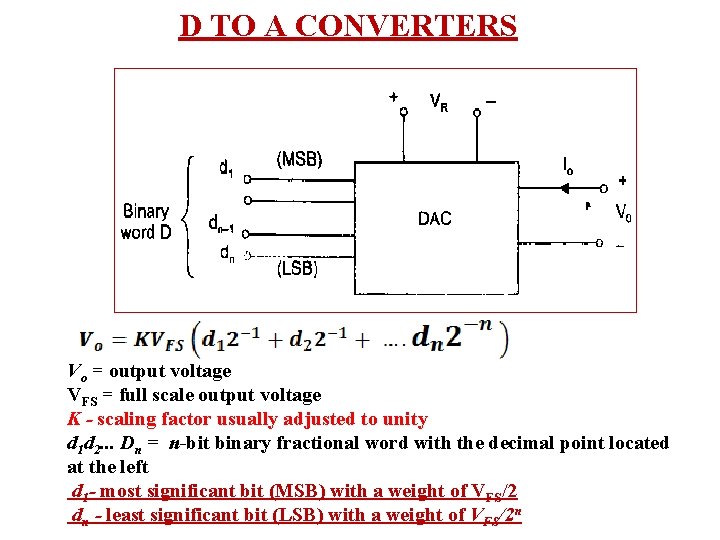
D TO A CONVERTERS Vo = output voltage VFS = full scale output voltage K - scaling factor usually adjusted to unity d 1 d 2. . . Dn = n-bit binary fractional word with the decimal point located at the left d 1 - most significant bit (MSB) with a weight of VFS/2 dn - least significant bit (LSB) with a weight of VFS/2 n

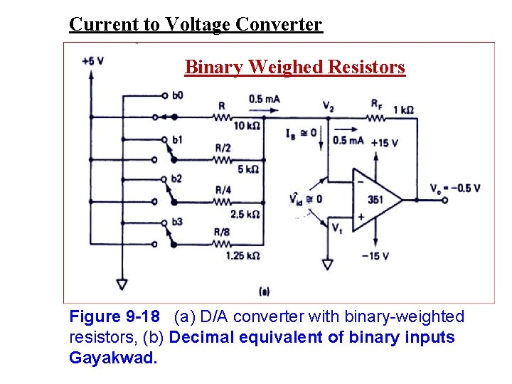
Current to Voltage Converter Binary Weighed Resistors Figure 9 -18 (a) D/A converter with binary-weighted resistors, (b) Decimal equivalent of binary inputs Gayakwad.

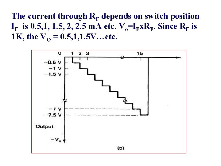
The current through RF depends on switch position IF is 0. 5, 1, 1. 5, 2, 2. 5 m. A etc. Vo=IFx. RF. Since RF is 1 K, the VO = 0. 5, 1, 1. 5 V…etc.

The important points to note down are When all the input bits are’ 0’, What is the minimum output Vo. ? Resolution = ± ½ LSB. When all the input bits are ‘ 1’ What is the output Vo. ? Maximum VO. What is the speed of conversion?

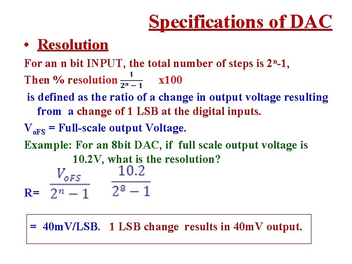
Specifications of DAC • Resolution For an n bit INPUT, the total number of steps is 2 n-1, Then % resolution x 100 is defined as the ratio of a change in output voltage resulting from a change of 1 LSB at the digital inputs. Vo. FS = Full-scale output Voltage. Example: For an 8 bit DAC, if full scale output voltage is 10. 2 V, what is the resolution? R= = 40 m. V/LSB. 1 LSB change results in 40 m. V output.

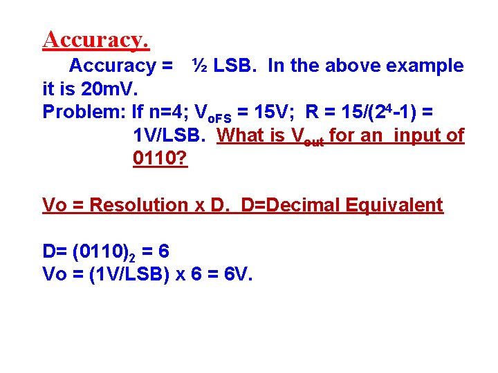
Accuracy = ½ LSB. In the above example it is 20 m. V. Problem: If n=4; Vo. FS = 15 V; R = 15/(24 -1) = 1 V/LSB. What is Vout for an input of 0110? Vo = Resolution x D. D=Decimal Equivalent D= (0110)2 = 6 Vo = (1 V/LSB) x 6 = 6 V.

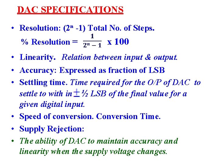
DAC SPECIFICATIONS • Resolution: (2 n -1) Total No. of Steps. % Resolution = x 100 • Linearity. Relation between input & output. • Accuracy: Expressed as fraction of LSB • Settling time. Time required for the O/P of DAC to settle to with in ½ LSB of the final value for a given digital input. • Speed of conversion. Conversion Time. • Supply Rejection: • The ability of DAC to maintain accuracy and linearity when the supply voltage changes.

Types of DAC 1. Binary weighted DAC 2. R-2 R ladder type DAC

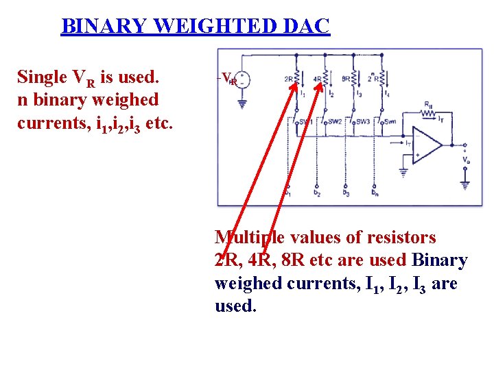
BINARY WEIGHTED DAC Single VR is used. n binary weighed currents, i 1, i 2, i 3 etc. -VR Multiple values of resistors 2 R, 4 R, 8 R etc are used Binary weighed currents, I 1, I 2, I 3 are used.

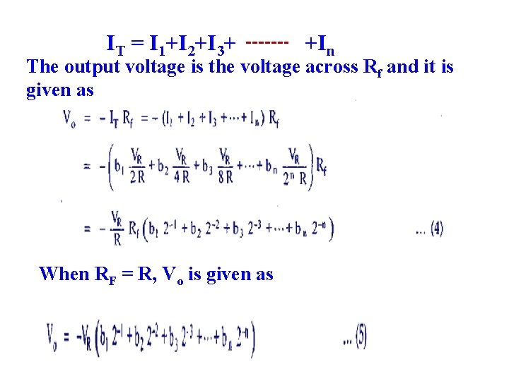
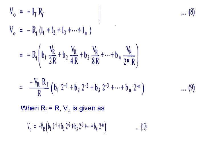
IT = I 1+I 2+I 3+ +In The output voltage is the voltage across Rf and it is given as When RF = R, Vo is given as

LIMITATIONS OF BINARY WEIGHTED RESISTORS (1) As the resolution increases, the resistor value increases. (2) Difficult to fabricate on chip. For an 8 bit DAC the largest resistor is 128 times the smallest one. (3) The accuracy is low, since depends on resistor values.

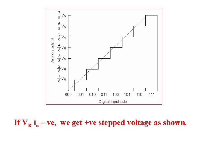
If VR ia – ve, we get +ve stepped voltage as shown.

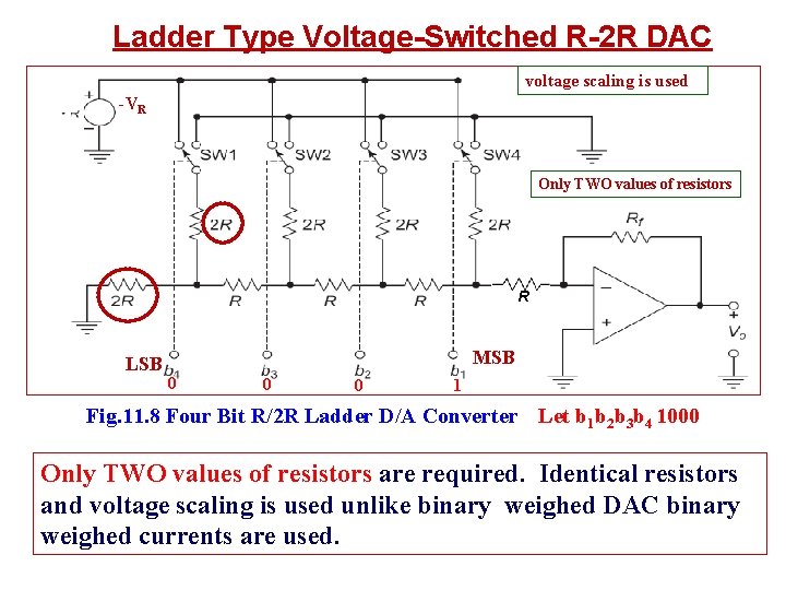
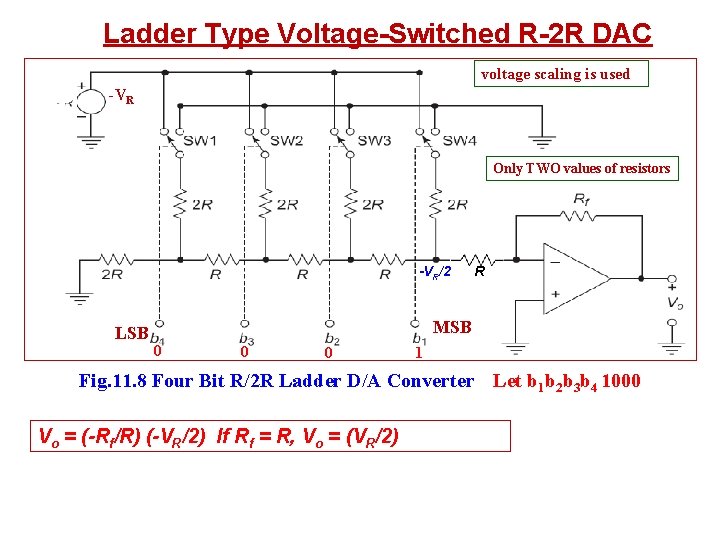
Ladder Type Voltage-Switched R-2 R DAC voltage scaling is used -VR Only TWO values of resistors R LSB MSB 0 0 0 1 Fig. 11. 8 Four Bit R/2 R Ladder D/A Converter Let b 1 b 2 b 3 b 4 1000 Only TWO values of resistors are required. Identical resistors and voltage scaling is used unlike binary weighed DAC binary weighed currents are used.

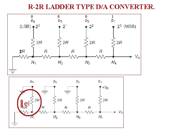
R-2 R LADDER TYPE D/A CONVERTER. 0 2 ║el 0 0 1


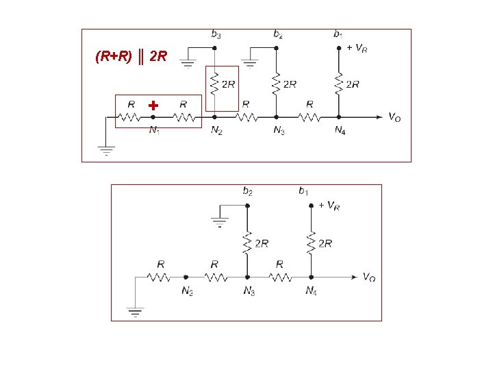
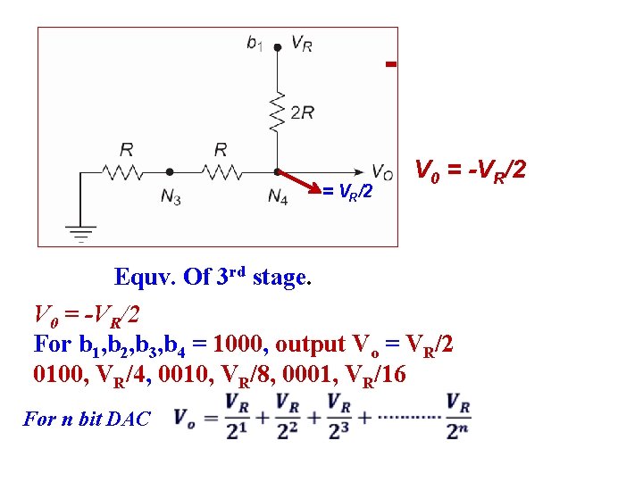
= VR/2 V 0 = -VR/2 Equv. Of 3 rd stage. V 0 = -VR/2 For b 1, b 2, b 3, b 4 = 1000, output Vo = VR/2 0100, VR/4, 0010, VR/8, 0001, VR/16 For n bit DAC

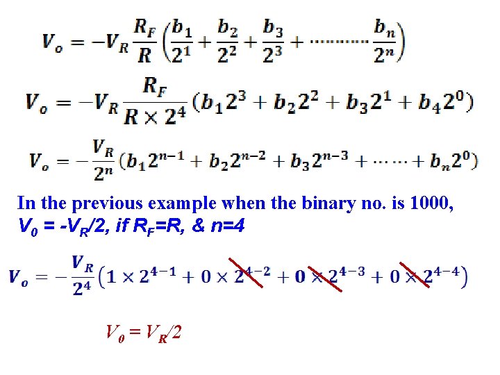
In the previous example when the binary no. is 1000, V 0 = -VR/2, if RF=R, & n=4 V 0 = VR/2

Ladder Type Voltage-Switched R-2 R DAC voltage scaling is used -VR Only TWO values of resistors -VR/2 LSB R MSB 0 0 0 1 Fig. 11. 8 Four Bit R/2 R Ladder D/A Converter Let b 1 b 2 b 3 b 4 1000 Vo = (-Rf/R) (-VR/2) If Rf = R, Vo = (VR/2)

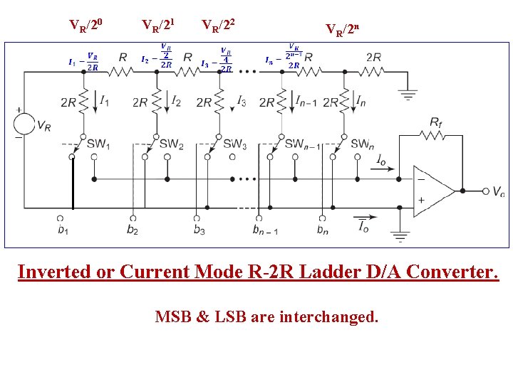
VR/20 VR/21 VR/22 VR/2 n Inverted or Current Mode R-2 R Ladder D/A Converter. MSB & LSB are interchanged.

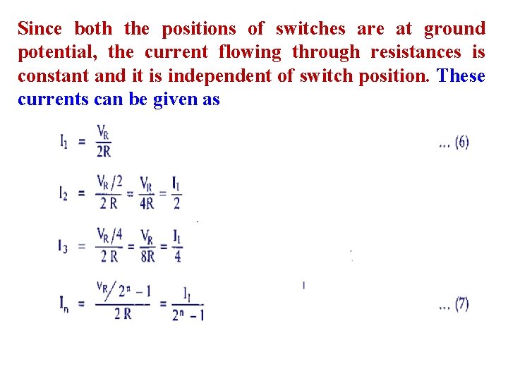
Since both the positions of switches are at ground potential, the current flowing through resistances is constant and it is independent of switch position. These currents can be given as

When Rf = R, Vo is given as

R-2 R LADDER TYPE DAC • Uses only two values of resistors • Overcomes the limitations of Binary weighted DAC • OPAMP is connected in inverting mode • Each digital input is applied through R-2 R network and Vref

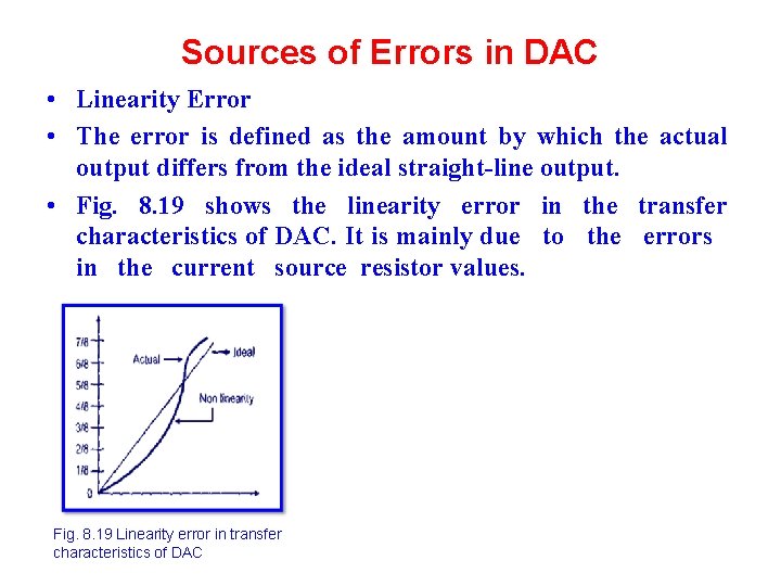
Sources of Errors in DAC • Linearity Error • The error is defined as the amount by which the actual output differs from the ideal straight-line output. • Fig. 8. 19 shows the linearity error in the transfer characteristics of DAC. It is mainly due to the errors in the current source resistor values. Fig. 8. 19 Linearity error in transfer characteristics of DAC

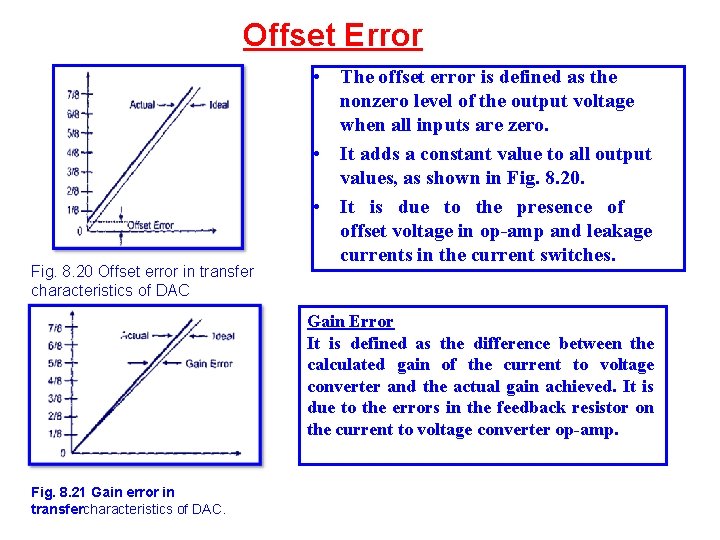
Offset Error Fig. 8. 20 Offset error in transfer characteristics of DAC • The offset error is defined as the nonzero level of the output voltage when all inputs are zero. • It adds a constant value to all output values, as shown in Fig. 8. 20. • It is due to the presence offset voltage in op-amp and leakage currents in the current switches. Gain Error It is defined as the difference between the calculated gain of the current to voltage converter and the actual gain achieved. It is due to the errors in the feedback resistor on the current to voltage converter op-amp. Fig. 8. 21 Gain error in transfercharacteristics of DAC.

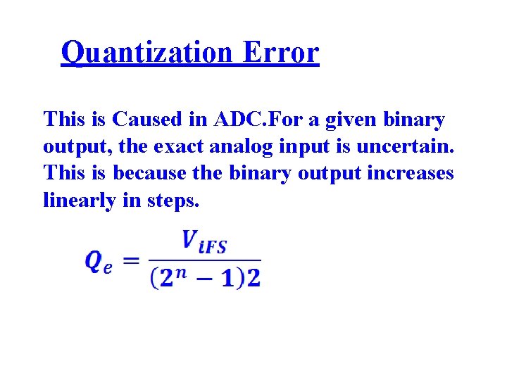
Quantization Error This is Caused in ADC. For a given binary output, the exact analog input is uncertain. This is because the binary output increases linearly in steps.

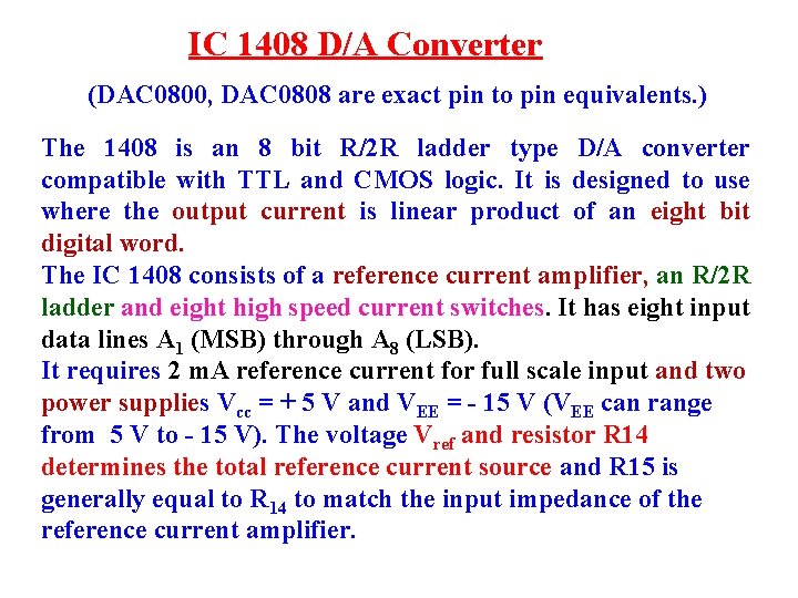
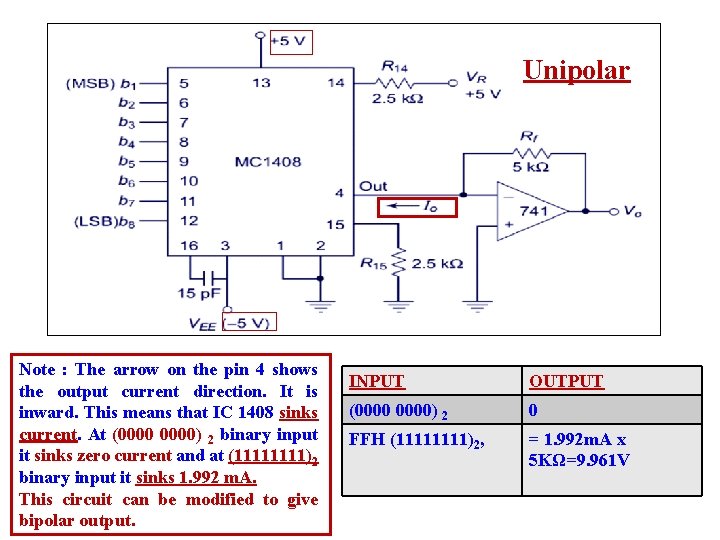
IC 1408 D/A Converter (DAC 0800, DAC 0808 are exact pin to pin equivalents. ) The 1408 is an 8 bit R/2 R ladder type D/A converter compatible with TTL and CMOS logic. It is designed to use where the output current is linear product of an eight bit digital word. The IC 1408 consists of a reference current amplifier, an R/2 R ladder and eight high speed current switches. It has eight input data lines A 1 (MSB) through A 8 (LSB). It requires 2 m. A reference current for full scale input and two power supplies Vcc = + 5 V and VEE = - 15 V (VEE can range from 5 V to - 15 V). The voltage Vref and resistor R 14 determines the total reference current source and R 15 is generally equal to R 14 to match the input impedance of the reference current amplifier.

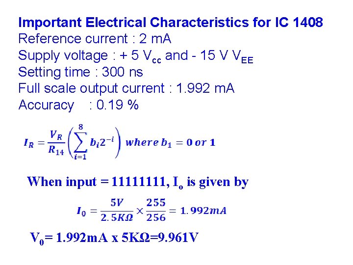
Important Electrical Characteristics for IC 1408 Reference current : 2 m. A Supply voltage : + 5 Vcc and - 15 V VEE Setting time : 300 ns Full scale output current : 1. 992 m. A Accuracy : 0. 19 % When input = 1111, Io is given by V 0= 1. 992 m. A x 5 KΩ=9. 961 V

Unipolar Note : The arrow on the pin 4 shows the output current direction. It is inward. This means that IC 1408 sinks current. At (0000) 2 binary input it sinks zero current and at (1111)2 binary input it sinks 1. 992 m. A. This circuit can be modified to give bipolar output. INPUT OUTPUT (0000) 2 0 FFH (1111)2, = 1. 992 m. A x 5 KΩ=9. 961 V

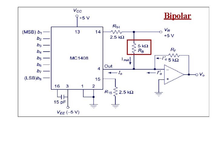
Bipolar

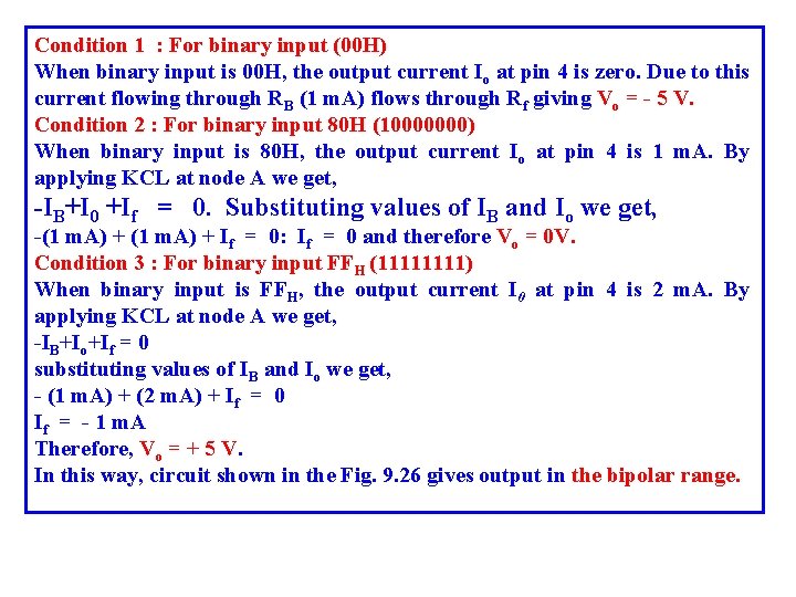
Condition 1 : For binary input (00 H) When binary input is 00 H, the output current Io at pin 4 is zero. Due to this current flowing through RB (1 m. A) flows through Rf giving Vo = - 5 V. Condition 2 : For binary input 80 H (10000000) When binary input is 80 H, the output current Io at pin 4 is 1 m. A. By applying KCL at node A we get, -IB+I 0 +If = 0. Substituting values of IB and Io we get, -(1 m. A) + If = 0: If = 0 and therefore Vo = 0 V. Condition 3 : For binary input FFH (1111) When binary input is FFH, the output current I 0 at pin 4 is 2 m. A. By applying KCL at node A we get, -IB+Io+If = 0 substituting values of IB and Io we get, - (1 m. A) + (2 m. A) + If = 0 If = - 1 m. A Therefore, Vo = + 5 V. In this way, circuit shown in the Fig. 9. 26 gives output in the bipolar range.

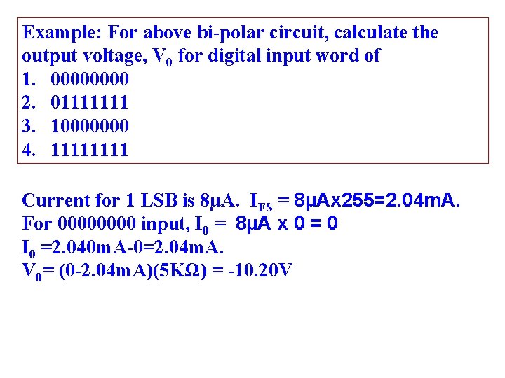
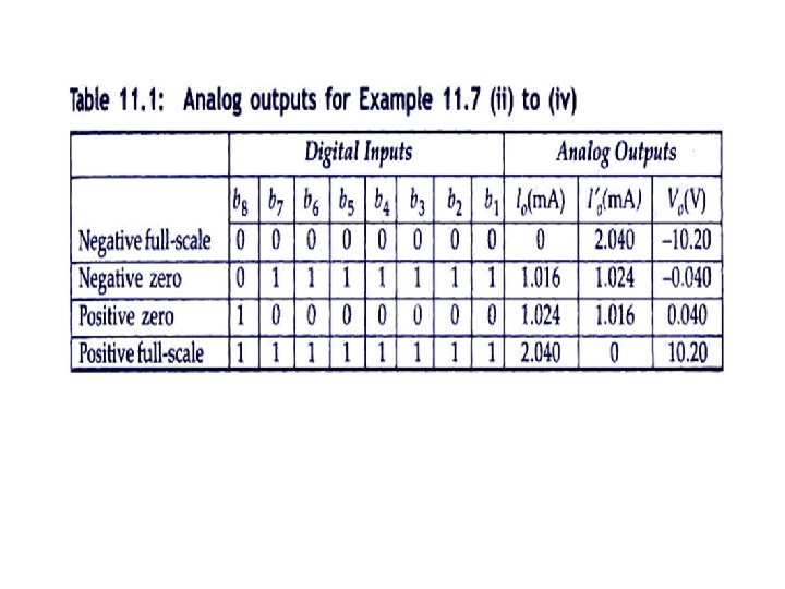
Example: For above bi-polar circuit, calculate the output voltage, V 0 for digital input word of 1. 0000 2. 01111111 3. 10000000 4. 1111 Current for 1 LSB is 8µA. IFS = 8µAx 255=2. 04 m. A. For 0000 input, I 0 = 8µA x 0 = 0 I 0 =2. 040 m. A-0=2. 04 m. A. V 0= (0 -2. 04 m. A)(5 KΩ) = -10. 20 V


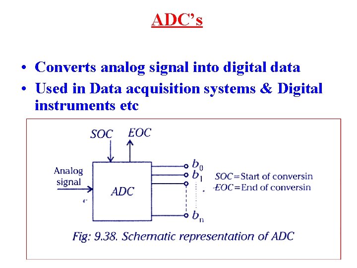
ADC’s • Converts analog signal into digital data • Used in Data acquisition systems & Digital instruments etc

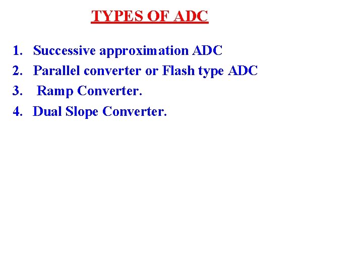
TYPES OF ADC 1. 2. 3. 4. Successive approximation ADC Parallel converter or Flash type ADC Ramp Converter. Dual Slope Converter.

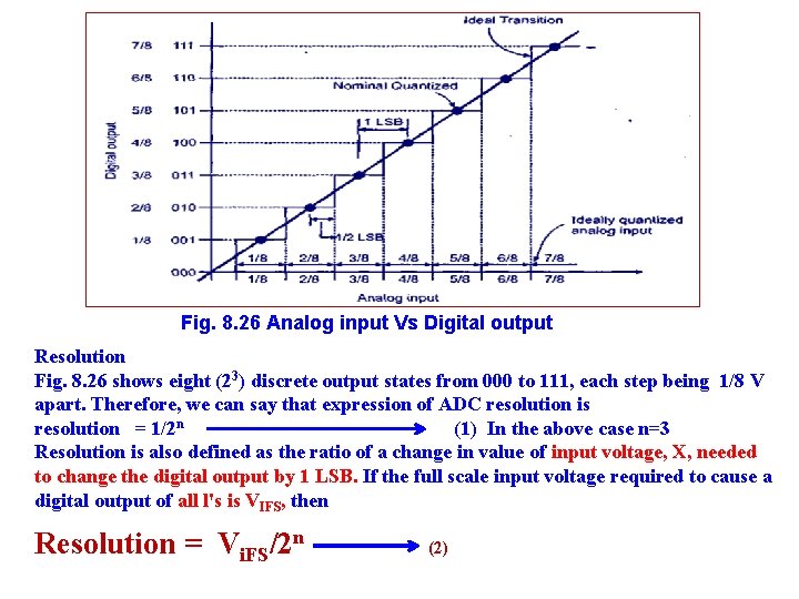
Fig. 8. 26 Analog input Vs Digital output Resolution Fig. 8. 26 shows eight (23) discrete output states from 000 to 111, each step being 1/8 V apart. Therefore, we can say that expression of ADC resolution is resolution = 1/2 n (1) In the above case n=3 Resolution is also defined as the ratio of a change in value of input voltage, X, needed to change the digital output by 1 LSB. If the full scale input voltage required to cause a digital output of all l's is VIFS, then Resolution = Vi. FS/2 n (2)

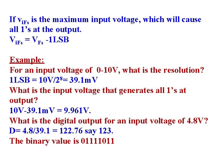
If vi. Fs is the maximum input voltage, which will cause all 1’s at the output. Vi. Fs = VFs -1 LSB Example: For an input voltage of 0 -10 V, what is the resolution? 1 LSB = 10 V/28= 39. 1 m. V What is the input voltage that generates all 1’s at output? 10 V-39. 1 m. V = 9. 961 V. What is the digital output for an input voltage of 4. 8 V? D= 4. 8/39. 1 = 122. 76 say 123. The binary value is 01111011

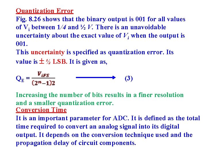
Quantization Error Fig. 8. 26 shows that the binary output is 001 for all values of Vi between 1/4 and ½ V. There is an unavoidable uncertainty about the exact value of Vi when the output is 001. This uncertainty is specified as quantization error. Its value is ½ LSB. It is given as, QE = (3) Increasing the number of bits results in a finer resolution and a smaller quantization error. Conversion Time It is an important parameter for ADC. It is defined as the total time required to convert an analog signal into its digital output. It depends on the conversion technique used and the propagation delay of circuit components.

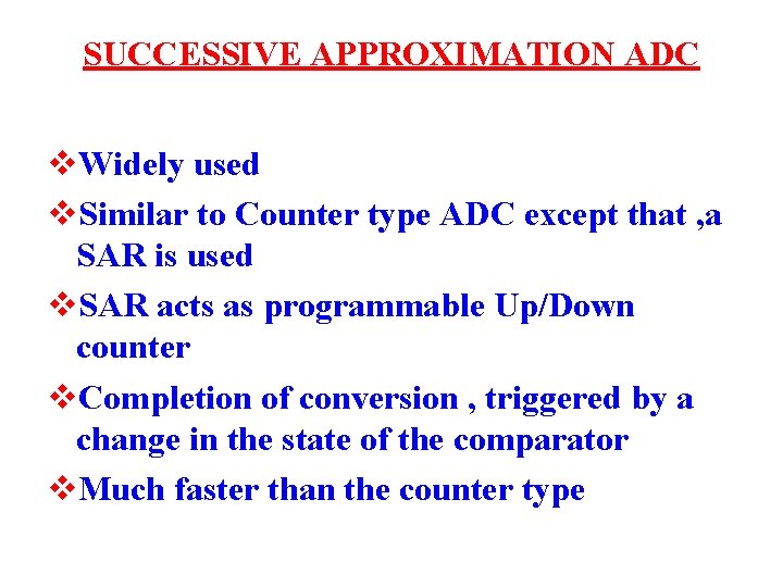
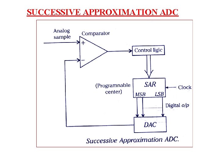
SUCCESSIVE APPROXIMATION ADC v. Widely used v. Similar to Counter type ADC except that , a SAR is used v. SAR acts as programmable Up/Down counter v. Completion of conversion , triggered by a change in the state of the comparator v. Much faster than the counter type

SUCCESSIVE APPROXIMATION ADC

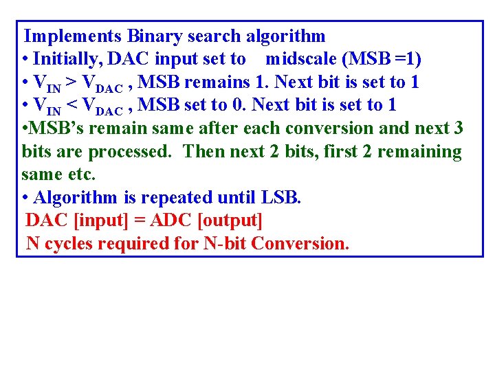
Implements Binary search algorithm • Initially, DAC input set to midscale (MSB =1) • VIN > VDAC , MSB remains 1. Next bit is set to 1 • VIN < VDAC , MSB set to 0. Next bit is set to 1 • MSB’s remain same after each conversion and next 3 bits are processed. Then next 2 bits, first 2 remaining same etc. • Algorithm is repeated until LSB. Typical accuracy levels of 8 to 12 bits. DAC [input] = ADC [output] N cycles required for N-bit Conversion.

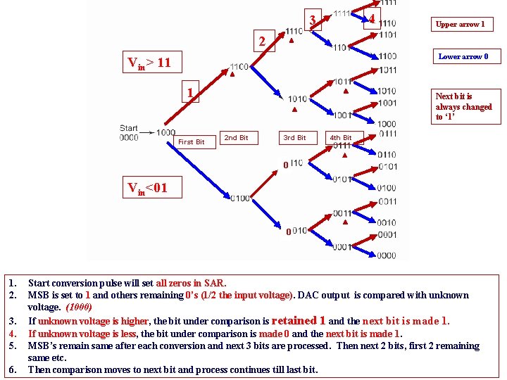
4 3 Upper arrow 1 2 Lower arrow 0 Vin> 11 1 First Bit Next bit is always changed to ‘ 1’ 2 nd Bit 3 rd Bit 4 th Bit 0 Vin<01 0 1. 2. 3. 4. 5. 6. Start conversion pulse will set all zeros in SAR. MSB is set to 1 and others remaining 0’s (1/2 the input voltage). DAC output is compared with unknown voltage. (1000) If unknown voltage is higher, the bit under comparison is retained 1 and the next bit is made 1. If unknown voltage is less, the bit under comparison is made 0 and the next bit is made 1. MSB’s remain same after each conversion and next 3 bits are processed. Then next 2 bits, first 2 remaining same etc. Then comparison moves to next bit and process continues till last bit.

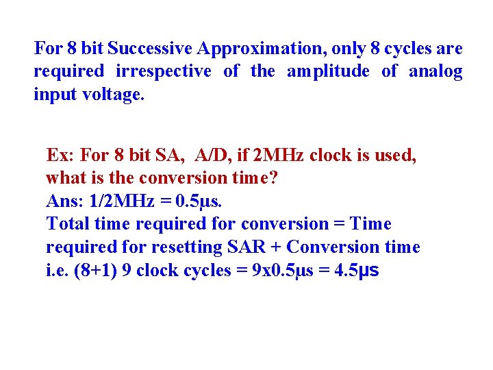
For 8 bit Successive Approximation, only 8 cycles are required irrespective of the amplitude of analog input voltage. Ex: For 8 bit SA, A/D, if 2 MHz clock is used, what is the conversion time? Ans: 1/2 MHz = 0. 5µs. Total time required for conversion = Time required for resetting SAR + Conversion time i. e. (8+1) 9 clock cycles = 9 x 0. 5µs = 4. 5µs

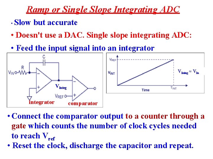
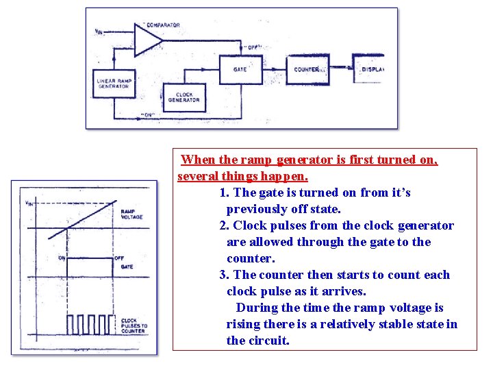
Ramp or Single Slope Integrating ADC • Slow but accurate • Doesn't use a DAC. Single slope integrating ADC: • Feed the input signal into an integrator Vinteg ≈ Vintegrator comparator • Connect the comparator output to a counter through a gate which counts the number of clock cycles needed to reach Vref • Reset the clock, discharge the capacitor and repeat.

When the ramp generator is first turned on, several things happen. 1. The gate is turned on from it’s previously off state. 2. Clock pulses from the clock generator are allowed through the gate to the counter. 3. The counter then starts to count each clock pulse as it arrives. During the time the ramp voltage is rising there is a relatively stable state in the circuit.

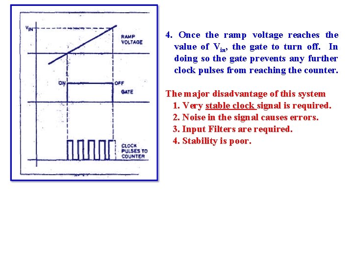
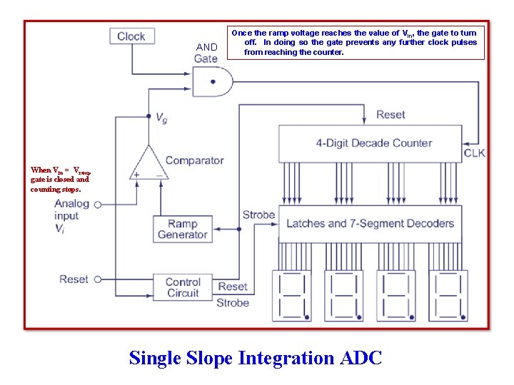
4. Once the ramp voltage reaches the value of Vin, the gate to turn off. In doing so the gate prevents any further clock pulses from reaching the counter. The major disadvantage of this system 1. Very stable clock signal is required. 2. Noise in the signal causes errors. 3. Input Filters are required. 4. Stability is poor.

AND Once the ramp voltage reaches the value of Vin, the gate to turn off. In doing so the gate prevents any further clock pulses from reaching the counter. When Vin = Vramp gate is closed and counting stops. Single Slope Integration ADC

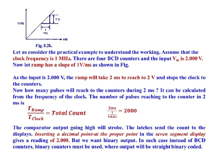
Fig. 8. 28.

The main limitations of this circuit are: i) Its resolution is less. Hence for applications which require resolution of 9 part in 20, 000 or more, this ADC is not stable. ii) Variations in ramp generator due to time, temperature or input voltage sensitivity also cause a lot of problems. • Big problem with single slope integration is calibration drift • The counting rate of the counter and the voltage slope of the integrator must always match each other exactly. • This puts a severe requirement on the stability and accuracy of the integrator (and also the comparator).

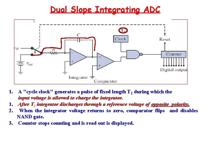
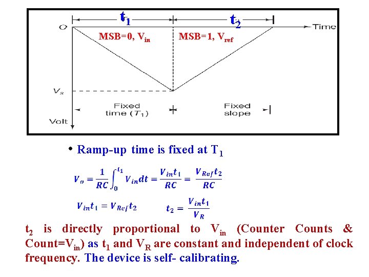
Dual Slope Integrating ADC T 1 1. A "cycle clock" generates a pulse of fixed length T 1 during which the input voltage is allowed to charge the integrator. 1. After T 1 integrator discharges through a reference voltage of opposite polarity. 2. When the integrator voltage returns to zero, comparator flips and disables NAND gate. 3. Counter stops counting and is read out is displayed.

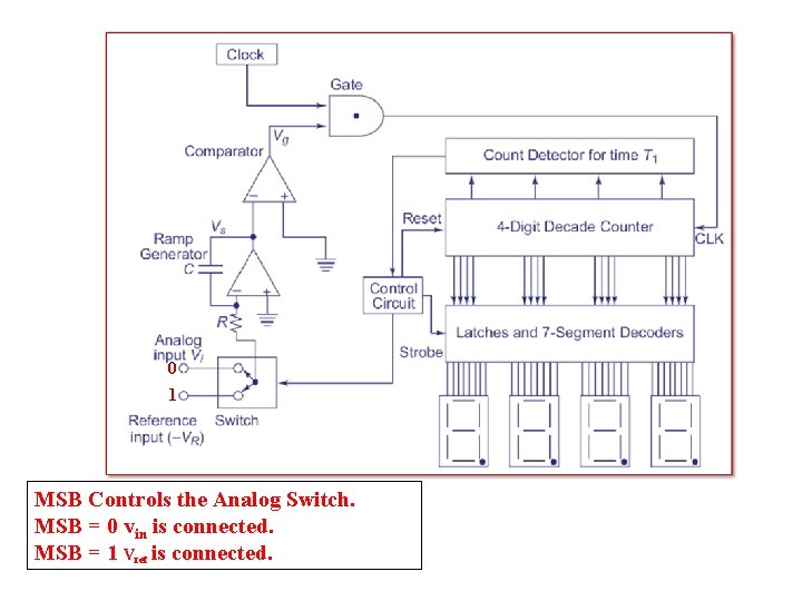
0 1 MSB Controls the Analog Switch. MSB = 0 vin is connected. MSB = 1 Vref is connected.

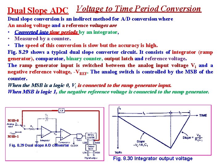
Dual Slope ADC Voltage to Time Period Conversion Dual slope conversion is an indirect method for A/D conversion where An analog voltage and a reference voltages are • Converted into time periods by an integrator, • Measured by a counter. • The speed of this conversion is slow but the accuracy is high. Fig. 8. 29 shows a typical dual slope converter circuit. It consists of integrator (ramp generator), comparator, binary counter, output latch and reference voltage. The ramp generator input is switched between the analog input voltage Vi and a negative reference voltage, -VREF. The analog switch is controlled by the MSB of the counter. When the MSB is a logic 0, Vi is connected to the ramp generator input. When MSB is logic 1, the negative reference voltage is connected to the ramp generator. MSB=0 MSB=1 Fig. 8. 29 Dual slope A/D converter Fig. 8. 30 Integrator output voltage

t 1 MSB=0, Vin t 2 MSB=1, Vref • Ramp-up time is fixed at T 1 t 2 is directly proportional to Vin (Counter Counts & Count=Vin) as t 1 and VR are constant and independent of clock frequency. The device is self- calibrating.

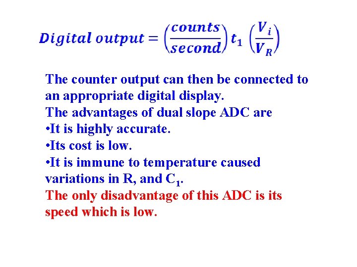
The counter output can then be connected to an appropriate digital display. The advantages of dual slope ADC are • It is highly accurate. • Its cost is low. • It is immune to temperature caused variations in R, and C 1. The only disadvantage of this ADC is its speed which is low.

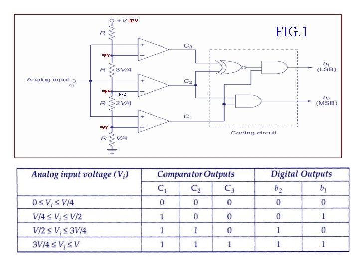
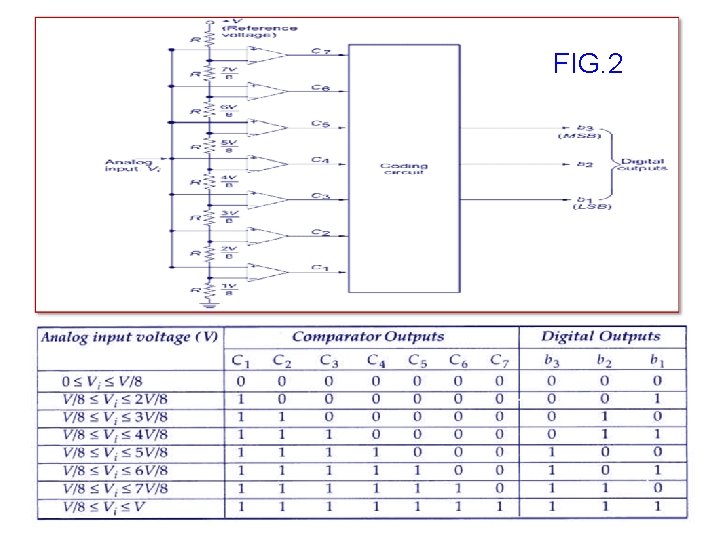
PARALLEL COMPERATOR FLASH ADC • For n-bit digital word, 2 n-1 comparators are required • The analog sample is simultaneously applied to one input (non-inverting) of all the comparators • Other input to the comparator is a DC voltage derived from the potential divider.

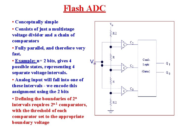
Flash ADC • Conceptually simple • Consists of just a multistage voltage divider and a chain of comparators • Fully parallel, and therefore very fast. • Example: n= 2 bits, gives 4 Vin possible states, representing 4 separate voltage intervals. • Analog input will fall into one of these intervals - we encode this assignment using the 2 bits • Defining the boundaries of 2 n intervals requires 2 n-1 comparators, with the threshold of each comparator set to the appropriate boundary voltage

=12 V FIG. 1 =9 V =6 V =3 V = V/2

FIG. 2

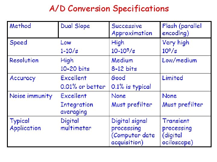
A/D Conversion Specifications

The time for one analog to digital conversion must depend on both the clock's period T and number of bits n. It is given as, Tc =T(n + 1) Where Tc = conversion time T=clock period n=number of bits Example -1 : An 8 bit successive approximation ADC is driven by a 1 MHz clock. Find its conversion time. Solution : f = 1 MHz; T=1/f = 1/106 = 1μSec. n=8 Tc = T(n+1) = 1(8+1) = 9 μSec.

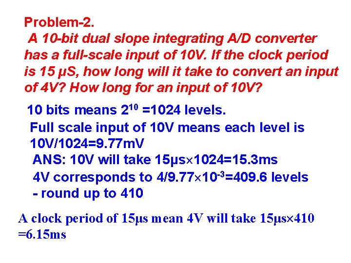
Problem-2. A 10 -bit dual slope integrating A/D converter has a full-scale input of 10 V. If the clock period is 15 μS, how long will it take to convert an input of 4 V? How long for an input of 10 V? 10 bits means 210 =1024 levels. Full scale input of 10 V means each level is 10 V/1024=9. 77 m. V ANS: 10 V will take 15μs 1024=15. 3 ms 4 V corresponds to 4/9. 77 10 -3=409. 6 levels - round up to 410 A clock period of 15μs mean 4 V will take 15μs 410 =6. 15 ms

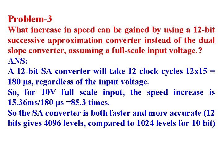
Problem-3 What increase in speed can be gained by using a 12 -bit successive approximation converter instead of the dual slope converter, assuming a full-scale input voltage. ? ANS: A 12 -bit SA converter will take 12 clock cycles 12 x 15 = 180 μs, regardless of the input voltage. So, for 10 V full scale input, the speed increase is 15. 36 ms/180 μs =85. 3 times. So the SA converter is both faster and more accurate (12 bits gives 4096 levels, compared to 1024 levels for 10 bit)

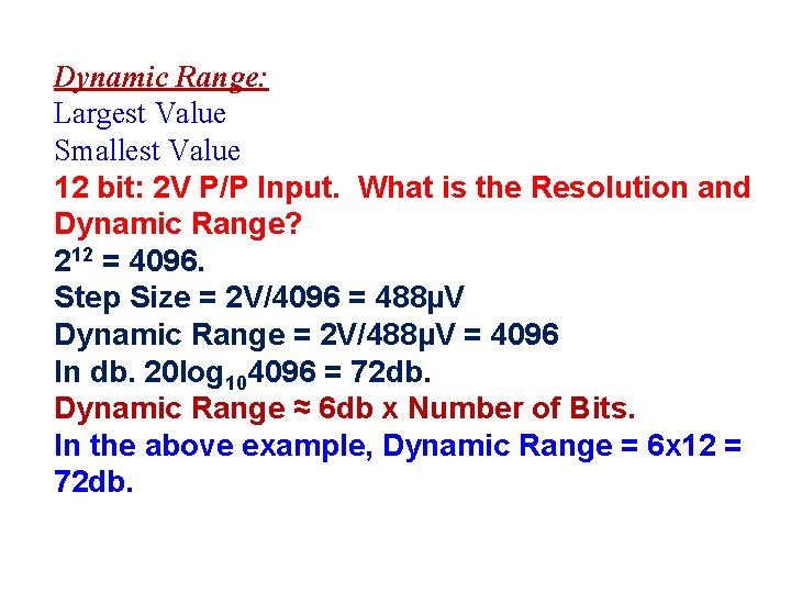
Dynamic Range: Largest Value Smallest Value 12 bit: 2 V P/P Input. What is the Resolution and Dynamic Range? 212 = 4096. Step Size = 2 V/4096 = 488µV Dynamic Range = 2 V/488µV = 4096 In db. 20 log 104096 = 72 db. Dynamic Range ≈ 6 db x Number of Bits. In the above example, Dynamic Range = 6 x 12 = 72 db.

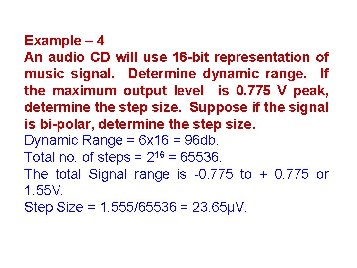
Example – 4 An audio CD will use 16 -bit representation of music signal. Determine dynamic range. If the maximum output level is 0. 775 V peak, determine the step size. Suppose if the signal is bi-polar, determine the step size. Dynamic Range = 6 x 16 = 96 db. Total no. of steps = 216 = 65536. The total Signal range is -0. 775 to + 0. 775 or 1. 55 V. Step Size = 1. 555/65536 = 23. 65µV.