Understanding Analog Performance Specifications Agenda ADC Operation ADC




![IDAC: Mode Details ¨ In its default mode (IDA 0 CN. [6: 4] = IDAC: Mode Details ¨ In its default mode (IDA 0 CN. [6: 4] =](https://slidetodoc.com/presentation_image_h/87ef0f9c2d67ce6cb16956b8a35b8196/image-73.jpg)



- Slides: 87

Understanding Analog Performance Specifications

Agenda ¨ ADC Operation ¨ ADC Performance Specifications ¨ IDAC Operation ¨ IDAC Performance Specifications ¨ System-Level Performance Measurement ¨ System-Level Error Compensation 2

ADC Operation

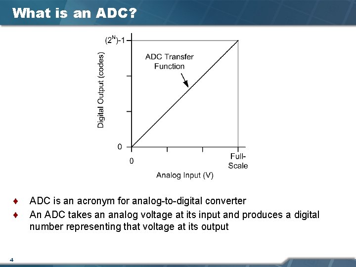
What is an ADC? ¨ ¨ 4 ADC is an acronym for analog-to-digital converter An ADC takes an analog voltage at its input and produces a digital number representing that voltage at its output

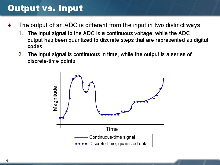
Output vs. Input ¨ The output of an ADC is different from the input in two distinct ways 1. The input signal to the ADC is a continuous voltage, while the ADC output has been quantized to discrete steps that are represented as digital codes 2. The input signal is continuous in time, while the output is a series of discrete-time points 5

ADC: Input Range ¨ An ADC’s input range is defined by the reference voltage (VREF) provided to the ADC ¨ The power supplies to the ADC are also important in determining the absolute input voltage Ø In most ADC architectures, input voltages outside the supply rails cannot be measured and may cause damage to the device 6

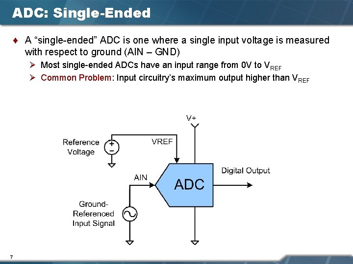
ADC: Single-Ended ¨ A “single-ended” ADC is one where a single input voltage is measured with respect to ground (AIN – GND) Ø Most single-ended ADCs have an input range from 0 V to VREF Ø Common Problem: Input circuitry’s maximum output higher than VREF 7

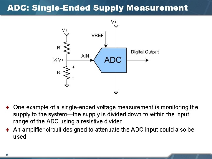
ADC: Single-Ended Supply Measurement ¨ One example of a single-ended voltage measurement is monitoring the supply to the system—the supply is divided down to within the input range of the ADC using a resistive divider ¨ An amplifier circuit designed to attenuate the ADC input could also be used 8

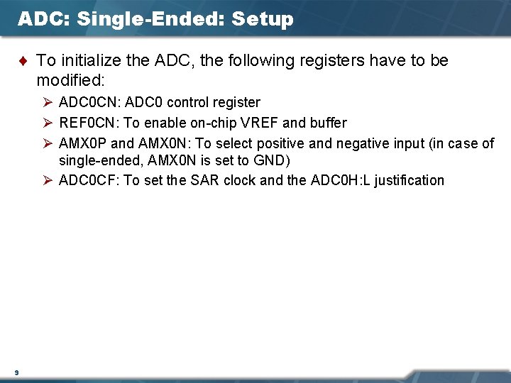
ADC: Single-Ended: Setup ¨ To initialize the ADC, the following registers have to be modified: Ø ADC 0 CN: ADC 0 control register Ø REF 0 CN: To enable on-chip VREF and buffer Ø AMX 0 P and AMX 0 N: To select positive and negative input (in case of single-ended, AMX 0 N is set to GND) Ø ADC 0 CF: To set the SAR clock and the ADC 0 H: L justification 9

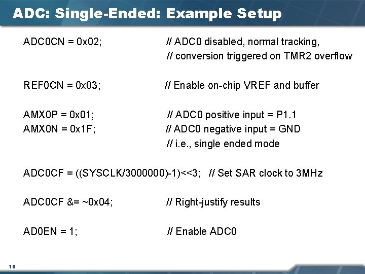
ADC: Single-Ended: Example Setup ADC 0 CN = 0 x 02; // ADC 0 disabled, normal tracking, // conversion triggered on TMR 2 overflow REF 0 CN = 0 x 03; // Enable on-chip VREF and buffer AMX 0 P = 0 x 01; AMX 0 N = 0 x 1 F; // ADC 0 positive input = P 1. 1 // ADC 0 negative input = GND // i. e. , single ended mode ADC 0 CF = ((SYSCLK/3000000)-1)<<3; // Set SAR clock to 3 MHz 10 ADC 0 CF &= ~0 x 04; // Right-justify results AD 0 EN = 1; // Enable ADC 0

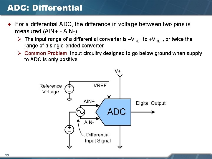
ADC: Differential ¨ For a differential ADC, the difference in voltage between two pins is measured (AIN+ - AIN-) Ø The input range of a differential converter is –VREF to +VREF, or twice the range of a single-ended converter Ø Common Problem: Input circuitry designed to go below ground when supply to ADC is only positive 11

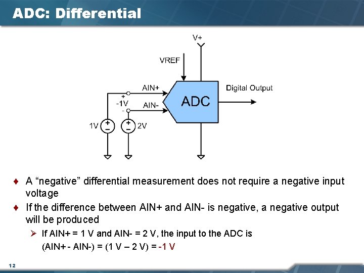
ADC: Differential ¨ A “negative” differential measurement does not require a negative input voltage ¨ If the difference between AIN+ and AIN- is negative, a negative output will be produced Ø If AIN+ = 1 V and AIN- = 2 V, the input to the ADC is (AIN+ - AIN-) = (1 V – 2 V) = -1 V 12

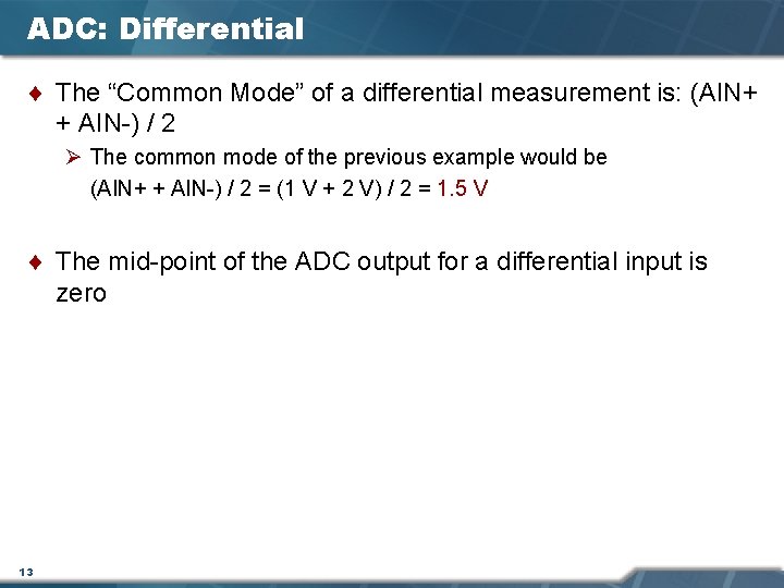
ADC: Differential ¨ The “Common Mode” of a differential measurement is: (AIN+ + AIN-) / 2 Ø The common mode of the previous example would be (AIN+ + AIN-) / 2 = (1 V + 2 V) / 2 = 1. 5 V ¨ The mid-point of the ADC output for a differential input is zero 13

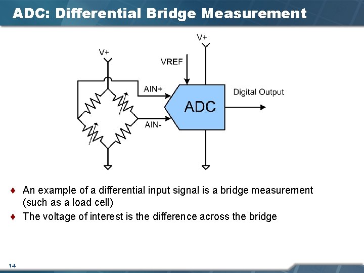
ADC: Differential Bridge Measurement ¨ An example of a differential input signal is a bridge measurement (such as a load cell) ¨ The voltage of interest is the difference across the bridge 14

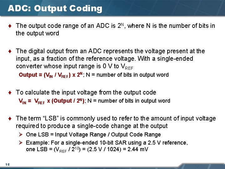
ADC: Output Coding ¨ The output code range of an ADC is 2 N, where N is the number of bits in the output word ¨ The digital output from an ADC represents the voltage present at the input, as a fraction of the reference voltage. With a single-ended converter whose input range is 0 V to VREF Output = (VIN / VREF) x 2 N; N = number of bits in output word ¨ To calculate the input voltage from the output code VIN = VREF x (Output / 2 N); N = number of bits in output word ¨ The term “LSB” is commonly used to refer to the amount of input voltage required to produce a single-code change at the output Ø One LSB = Input Voltage Range / Output Code Range Ø Example: For a single-ended 10 -bit SAR using a 2. 5 V reference, one LSB = (VREF / 210) = (2. 5 V / 1024) = 2. 44 m. V 15

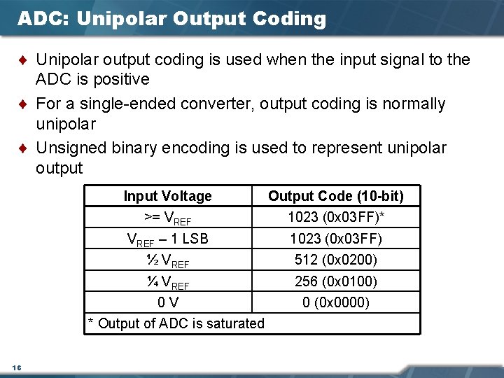
ADC: Unipolar Output Coding ¨ Unipolar output coding is used when the input signal to the ADC is positive ¨ For a single-ended converter, output coding is normally unipolar ¨ Unsigned binary encoding is used to represent unipolar output Input Voltage Output Code (10 -bit) >= VREF 1023 (0 x 03 FF)* VREF – 1 LSB 1023 (0 x 03 FF) ½ VREF 512 (0 x 0200) ¼ VREF 256 (0 x 0100) 0 V 0 (0 x 0000) * Output of ADC is saturated 16

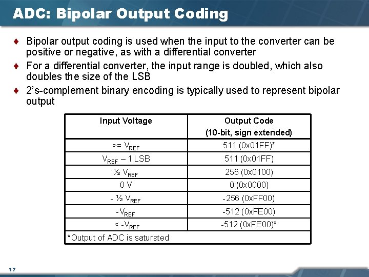
ADC: Bipolar Output Coding ¨ Bipolar output coding is used when the input to the converter can be positive or negative, as with a differential converter ¨ For a differential converter, the input range is doubled, which also doubles the size of the LSB ¨ 2’s-complement binary encoding is typically used to represent bipolar output Input Voltage Output Code (10 -bit, sign extended) >= VREF 511 (0 x 01 FF)* VREF – 1 LSB 511 (0 x 01 FF) ½ VREF 256 (0 x 0100) 0 V 0 (0 x 0000) - ½ VREF -256 (0 x. FF 00) -VREF -512 (0 x. FE 00) < -VREF -512 (0 x. FE 00)* *Output of ADC is saturated 17

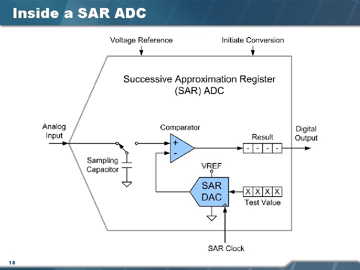
Inside a SAR ADC 18

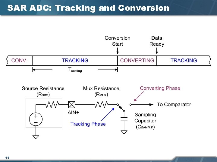
SAR ADC: Tracking and Conversion 19

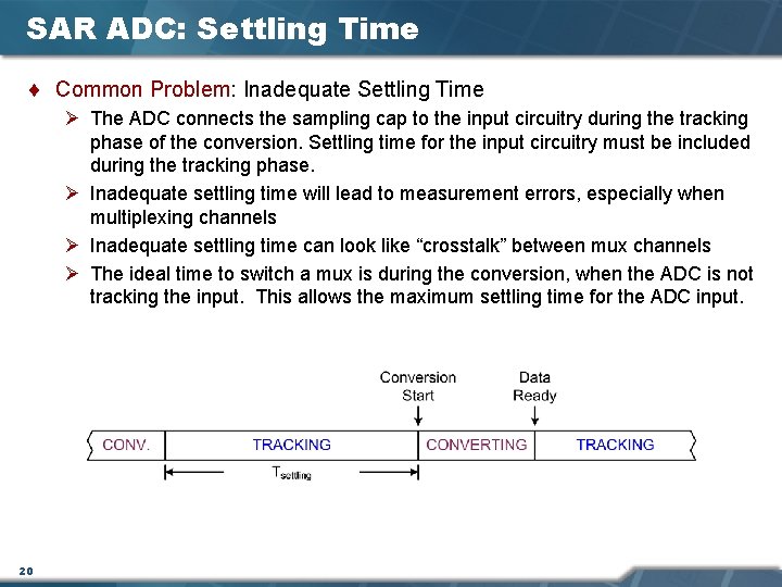
SAR ADC: Settling Time ¨ Common Problem: Inadequate Settling Time Ø The ADC connects the sampling cap to the input circuitry during the tracking phase of the conversion. Settling time for the input circuitry must be included during the tracking phase. Ø Inadequate settling time will lead to measurement errors, especially when multiplexing channels Ø Inadequate settling time can look like “crosstalk” between mux channels Ø The ideal time to switch a mux is during the conversion, when the ADC is not tracking the input. This allows the maximum settling time for the ADC input. 20

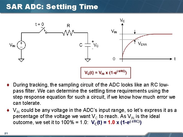
SAR ADC: Settling Time ¨ During tracking, the sampling circuit of the ADC looks like an RC lowpass filter. We can determine the settling time requirements using the step response equation for such a circuit, if we know how much error we can tolerate. ¨ VIN could be any voltage in the ADC’s input range, so let’s express it as a percentage of the voltage we want VC to reach. As VIN is the ideal outcome, we set it to 100% = 1. 0: VC(t) = 1. 0 x (1 -e(-t/RC)) 21

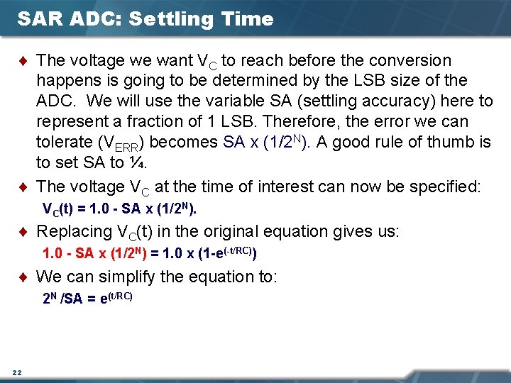
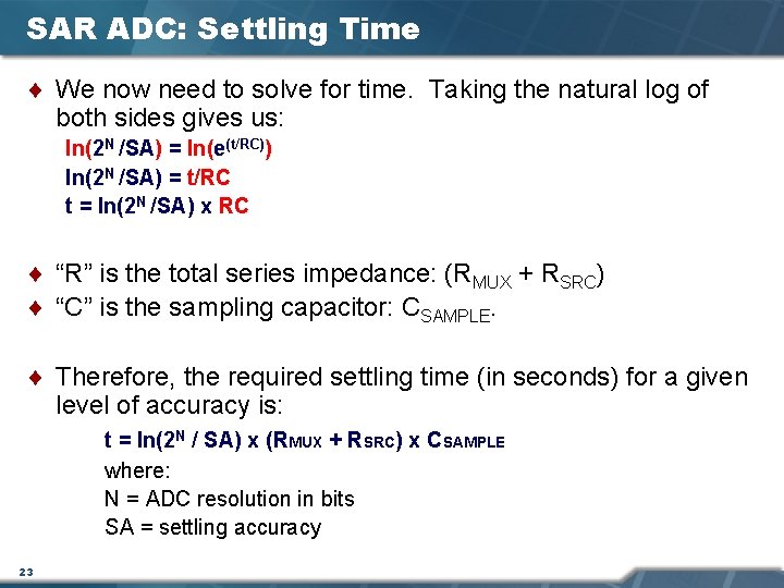
SAR ADC: Settling Time ¨ The voltage we want VC to reach before the conversion happens is going to be determined by the LSB size of the ADC. We will use the variable SA (settling accuracy) here to represent a fraction of 1 LSB. Therefore, the error we can tolerate (VERR) becomes SA x (1/2 N). A good rule of thumb is to set SA to ¼. ¨ The voltage VC at the time of interest can now be specified: VC(t) = 1. 0 - SA x (1/2 N). ¨ Replacing VC(t) in the original equation gives us: 1. 0 - SA x (1/2 N) = 1. 0 x (1 -e(-t/RC)) ¨ We can simplify the equation to: 2 N /SA = e(t/RC) 22

SAR ADC: Settling Time ¨ We now need to solve for time. Taking the natural log of both sides gives us: ln(2 N /SA) = ln(e(t/RC)) ln(2 N /SA) = t/RC t = ln(2 N /SA) x RC ¨ “R” is the total series impedance: (RMUX + RSRC) ¨ “C” is the sampling capacitor: CSAMPLE. ¨ Therefore, the required settling time (in seconds) for a given level of accuracy is: t = ln(2 N / SA) x (RMUX + RSRC) x CSAMPLE where: N = ADC resolution in bits SA = settling accuracy 23

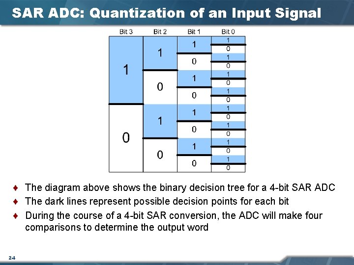
SAR ADC: Quantization of an Input Signal ¨ The diagram above shows the binary decision tree for a 4 -bit SAR ADC ¨ The dark lines represent possible decision points for each bit ¨ During the course of a 4 -bit SAR conversion, the ADC will make four comparisons to determine the output word 24

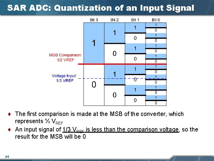
SAR ADC: Quantization of an Input Signal ¨ The first comparison is made at the MSB of the converter, which represents ½ VREF ¨ An input signal of 1/3 VREF is less than the comparison voltage, so the result for the MSB will be 0 25

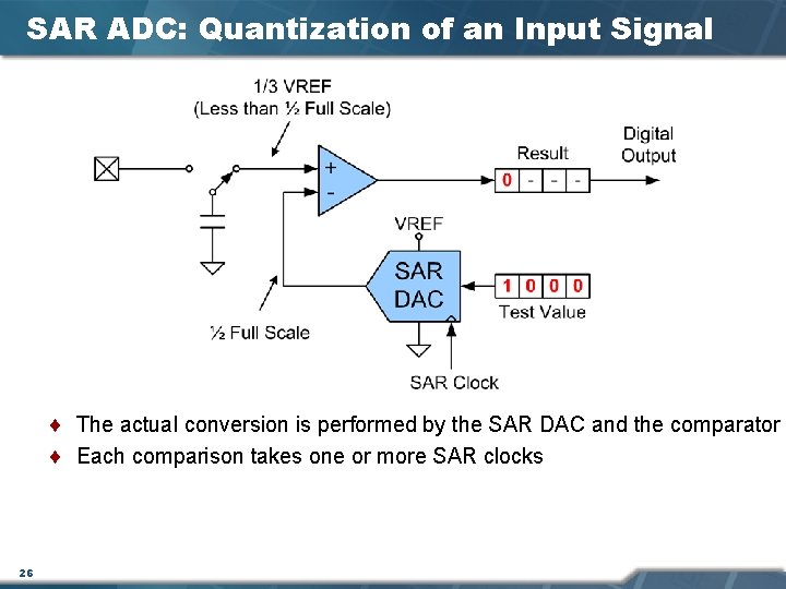
SAR ADC: Quantization of an Input Signal ¨ The actual conversion is performed by the SAR DAC and the comparator ¨ Each comparison takes one or more SAR clocks 26

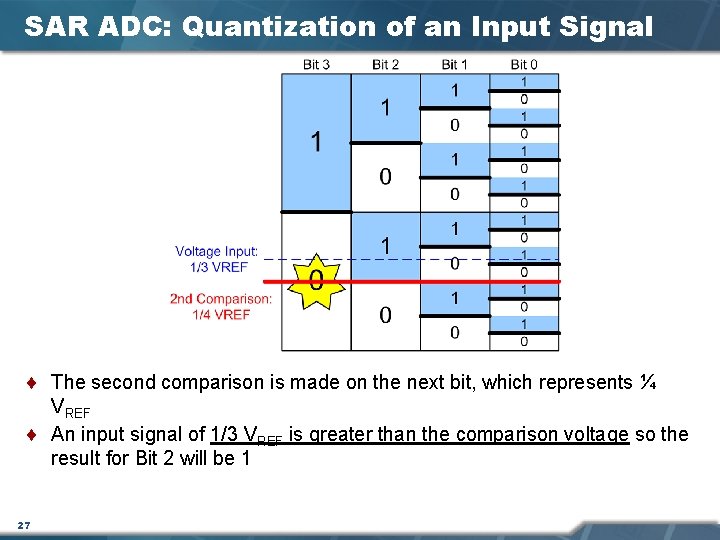
SAR ADC: Quantization of an Input Signal ¨ The second comparison is made on the next bit, which represents ¼ VREF ¨ An input signal of 1/3 VREF is greater than the comparison voltage so the result for Bit 2 will be 1 27

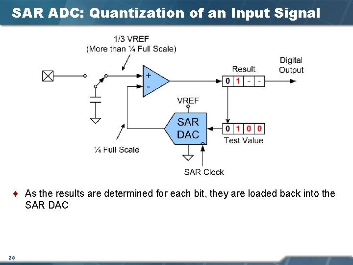
SAR ADC: Quantization of an Input Signal ¨ As the results are determined for each bit, they are loaded back into the SAR DAC 28

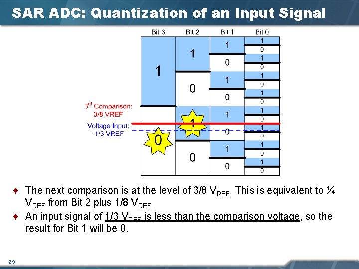
SAR ADC: Quantization of an Input Signal ¨ The next comparison is at the level of 3/8 VREF. This is equivalent to ¼ VREF from Bit 2 plus 1/8 VREF. ¨ An input signal of 1/3 VREF is less than the comparison voltage, so the result for Bit 1 will be 0. 29

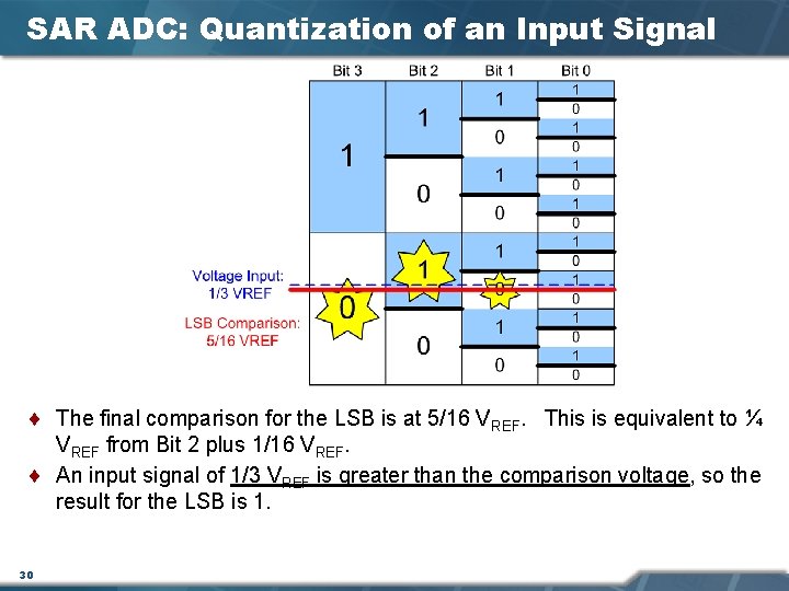
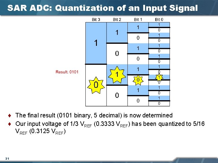
SAR ADC: Quantization of an Input Signal ¨ The final comparison for the LSB is at 5/16 VREF. This is equivalent to ¼ VREF from Bit 2 plus 1/16 VREF. ¨ An input signal of 1/3 VREF is greater than the comparison voltage, so the result for the LSB is 1. 30

SAR ADC: Quantization of an Input Signal ¨ The final result (0101 binary, 5 decimal) is now determined ¨ Our input voltage of 1/3 VREF (0. 3333 VREF) has been quantized to 5/16 VREF (0. 3125 VREF) 31

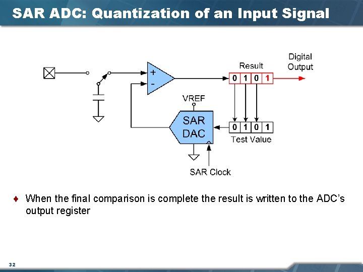
SAR ADC: Quantization of an Input Signal ¨ When the final comparison is complete the result is written to the ADC’s output register 32

SAR ADC: Conversion Time ¨ The conversion time required by the ADC is determined by the speed of the SAR clock ¨ The SAR clock speed does not determine output word rate (this is determined by the start-of-conversion source) ¨ Common Problem: SAR clock is too fast Ø Running a SAR with a clock that is too fast will lead to settling time problems with the internal SAR DAC Ø This will generally look like a linearity or missing code problem Ø The SAR Clock should be as close to the maximum specification as possible, but not faster—this minimizes conversion time and allows for maximum input tracking time 33

ADC Specifications

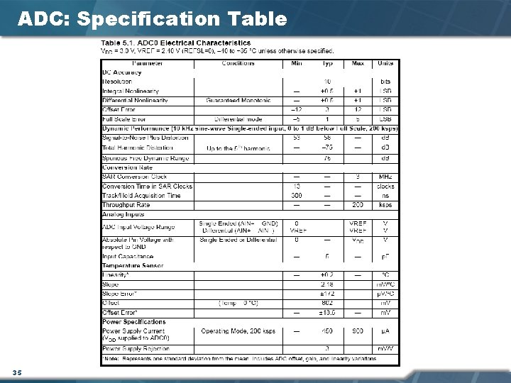
ADC: Specification Table 35

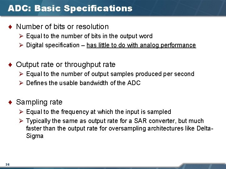
ADC: Basic Specifications ¨ Number of bits or resolution Ø Equal to the number of bits in the output word Ø Digital specification – has little to do with analog performance ¨ Output rate or throughput rate Ø Equal to the number of output samples produced per second Ø Defines the usable bandwidth of the ADC ¨ Sampling rate Ø Equal to the frequency at which the input is sampled Ø Typically the same as output rate for a SAR converter, but much faster than the output rate for oversampling architectures like Delta. Sigma 36

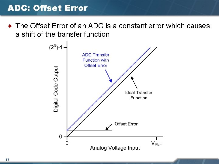
ADC: Offset Error ¨ The Offset Error of an ADC is a constant error which causes a shift of the transfer function 37

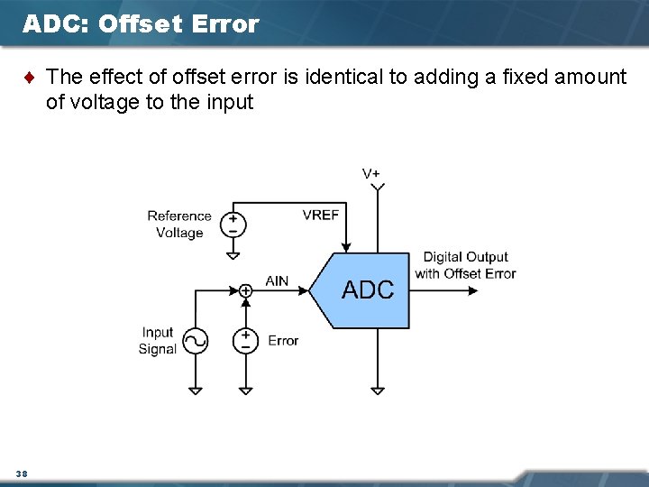
ADC: Offset Error ¨ The effect of offset error is identical to adding a fixed amount of voltage to the input 38

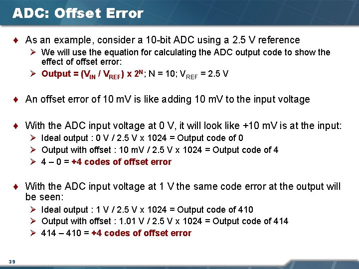
ADC: Offset Error ¨ As an example, consider a 10 -bit ADC using a 2. 5 V reference Ø We will use the equation for calculating the ADC output code to show the effect of offset error: Ø Output = (VIN / VREF) x 2 N; N = 10; VREF = 2. 5 V ¨ An offset error of 10 m. V is like adding 10 m. V to the input voltage ¨ With the ADC input voltage at 0 V, it will look like +10 m. V is at the input: Ø Ideal output : 0 V / 2. 5 V x 1024 = Output code of 0 Ø Output with offset : 10 m. V / 2. 5 V x 1024 = Output code of 4 Ø 4 – 0 = +4 codes of offset error ¨ With the ADC input voltage at 1 V the same code error at the output will be seen: Ø Ideal output : 1 V / 2. 5 V x 1024 = Output code of 410 Ø Output with offset : 1. 01 V / 2. 5 V x 1024 = Output code of 414 Ø 414 – 410 = +4 codes of offset error 39

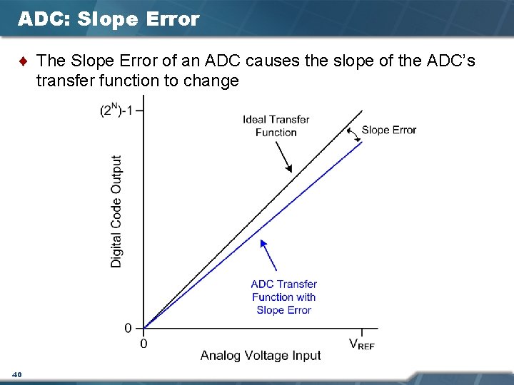
ADC: Slope Error ¨ The Slope Error of an ADC causes the slope of the ADC’s transfer function to change 40

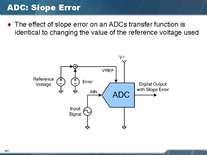
ADC: Slope Error ¨ The effect of slope error on an ADCs transfer function is identical to changing the value of the reference voltage used 41

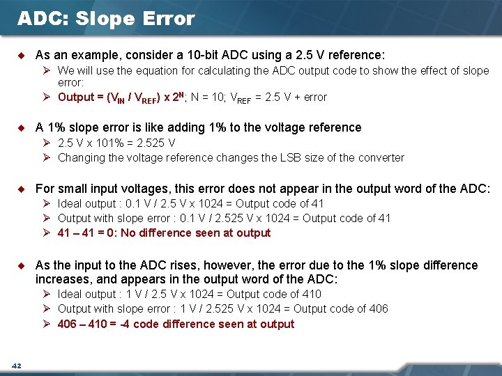
ADC: Slope Error ¨ As an example, consider a 10 -bit ADC using a 2. 5 V reference: Ø We will use the equation for calculating the ADC output code to show the effect of slope error: Ø Output = (VIN / VREF) x 2 N; N = 10; VREF = 2. 5 V + error ¨ A 1% slope error is like adding 1% to the voltage reference Ø 2. 5 V x 101% = 2. 525 V Ø Changing the voltage reference changes the LSB size of the converter ¨ For small input voltages, this error does not appear in the output word of the ADC: Ø Ideal output : 0. 1 V / 2. 5 V x 1024 = Output code of 41 Ø Output with slope error : 0. 1 V / 2. 525 V x 1024 = Output code of 41 Ø 41 – 41 = 0: No difference seen at output ¨ As the input to the ADC rises, however, the error due to the 1% slope difference increases, and appears in the output word of the ADC: Ø Ideal output : 1 V / 2. 5 V x 1024 = Output code of 410 Ø Output with slope error : 1 V / 2. 525 V x 1024 = Output code of 406 Ø 406 – 410 = -4 code difference seen at output 42

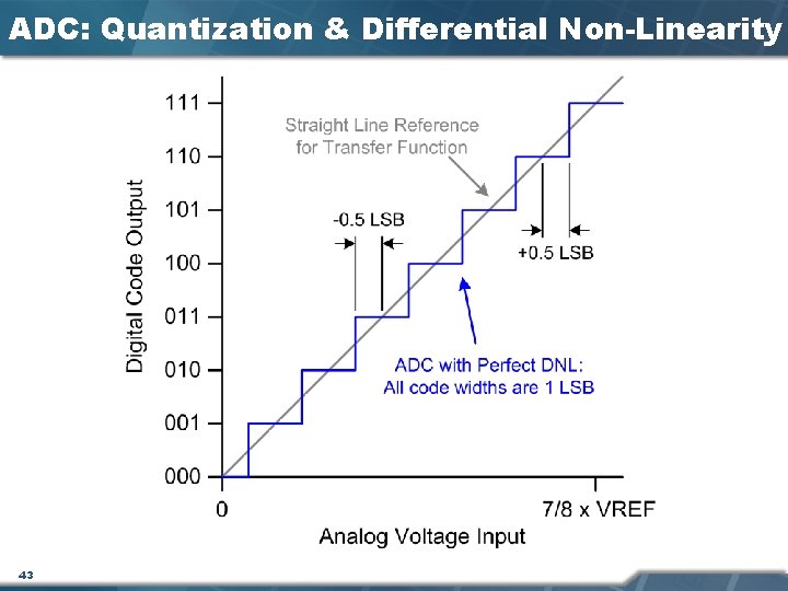
ADC: Quantization & Differential Non-Linearity 43

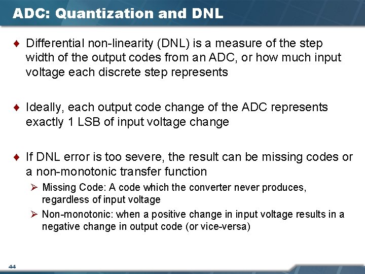
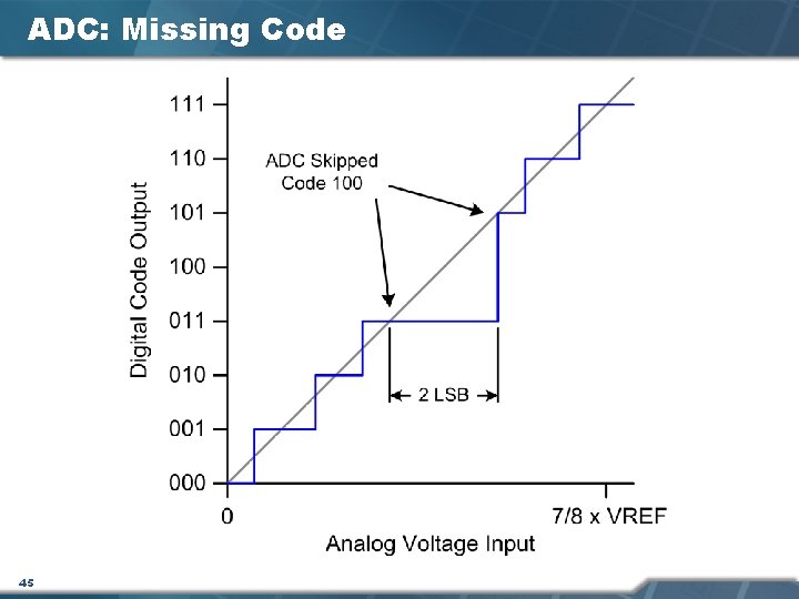
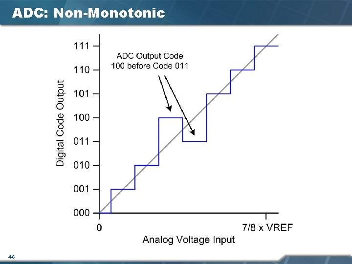
ADC: Quantization and DNL ¨ Differential non-linearity (DNL) is a measure of the step width of the output codes from an ADC, or how much input voltage each discrete step represents ¨ Ideally, each output code change of the ADC represents exactly 1 LSB of input voltage change ¨ If DNL error is too severe, the result can be missing codes or a non-monotonic transfer function Ø Missing Code: A code which the converter never produces, regardless of input voltage Ø Non-monotonic: when a positive change in input voltage results in a negative change in output code (or vice-versa) 44

ADC: Missing Code 45

ADC: Non-Monotonic 46

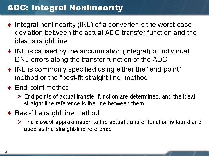
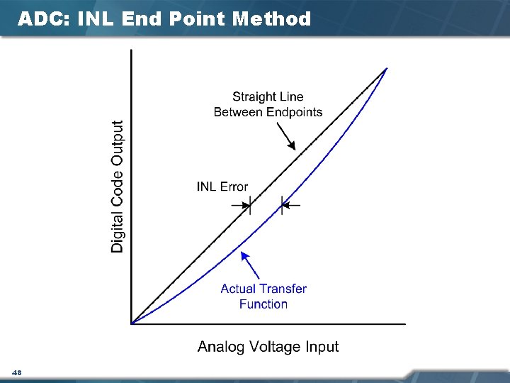
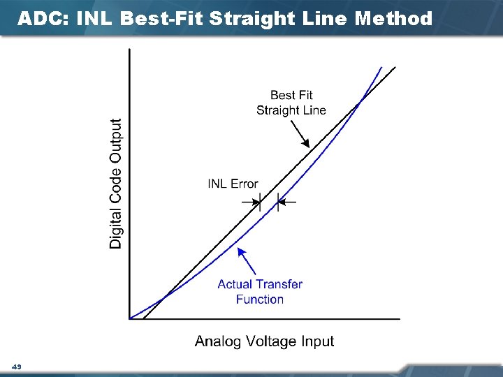
ADC: Integral Nonlinearity ¨ Integral nonlinearity (INL) of a converter is the worst-case deviation between the actual ADC transfer function and the ideal straight line ¨ INL is caused by the accumulation (integral) of individual DNL errors along the transfer function of the ADC ¨ INL is commonly specified using either the “end-point” method or the “best-fit straight line” method ¨ End point method Ø End points of actual transfer function are determined, and the ideal straight-line reference is the line between them ¨ Best-fit straight line method Ø The closest approximation to the actual transfer function is found and used as the straight-line reference 47

ADC: INL End Point Method 48

ADC: INL Best-Fit Straight Line Method 49

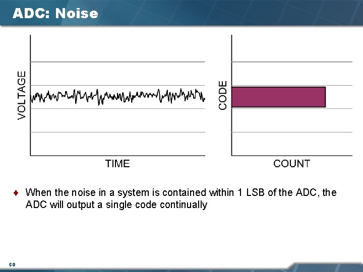
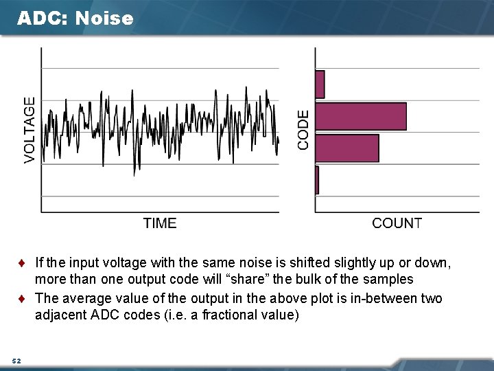
ADC: Noise ¨ When the noise in a system is contained within 1 LSB of the ADC, the ADC will output a single code continually 50

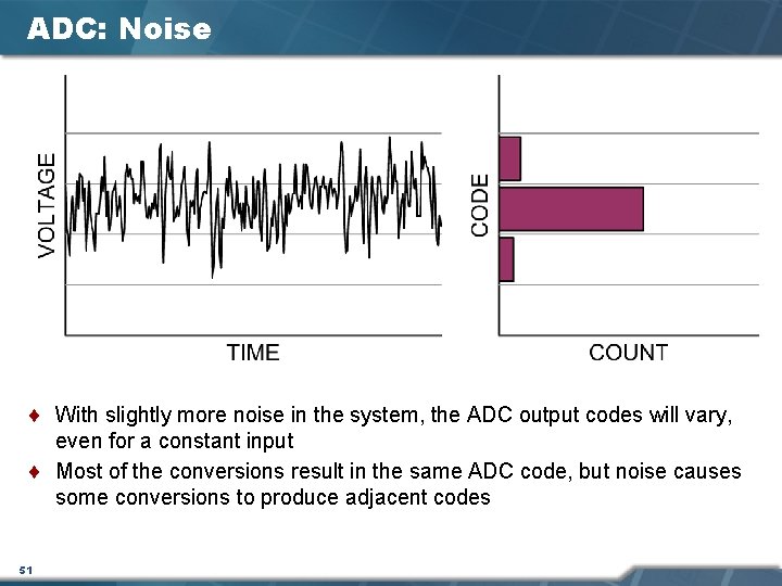
ADC: Noise ¨ With slightly more noise in the system, the ADC output codes will vary, even for a constant input ¨ Most of the conversions result in the same ADC code, but noise causes some conversions to produce adjacent codes 51

ADC: Noise ¨ If the input voltage with the same noise is shifted slightly up or down, more than one output code will “share” the bulk of the samples ¨ The average value of the output in the above plot is in-between two adjacent ADC codes (i. e. a fractional value) 52

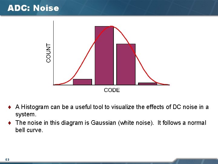
ADC: Noise ¨ A Histogram can be a useful tool to visualize the effects of DC noise in a system. ¨ The noise in this diagram is Gaussian (white noise). It follows a normal bell curve. 53

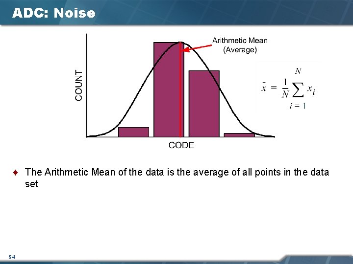
ADC: Noise ¨ The Arithmetic Mean of the data is the average of all points in the data set 54

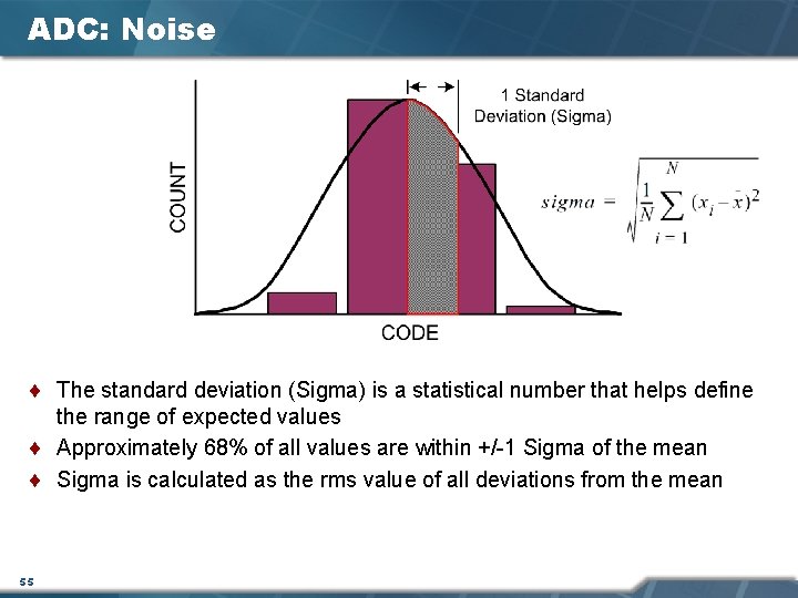
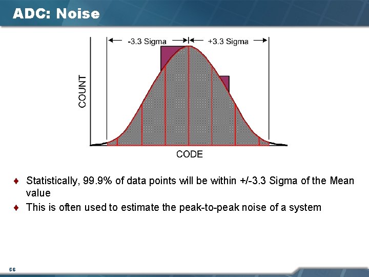
ADC: Noise ¨ The standard deviation (Sigma) is a statistical number that helps define the range of expected values ¨ Approximately 68% of all values are within +/-1 Sigma of the mean ¨ Sigma is calculated as the rms value of all deviations from the mean 55

ADC: Noise ¨ Statistically, 99. 9% of data points will be within +/-3. 3 Sigma of the Mean value ¨ This is often used to estimate the peak-to-peak noise of a system 56

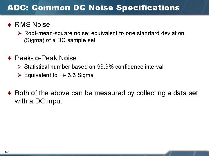
ADC: Common DC Noise Specifications ¨ RMS Noise Ø Root-mean-square noise: equivalent to one standard deviation (Sigma) of a DC sample set ¨ Peak-to-Peak Noise Ø Statistical number based on 99. 9% confidence interval Ø Equivalent to +/- 3. 3 Sigma ¨ Both of the above can be measured by collecting a data set with a DC input 57

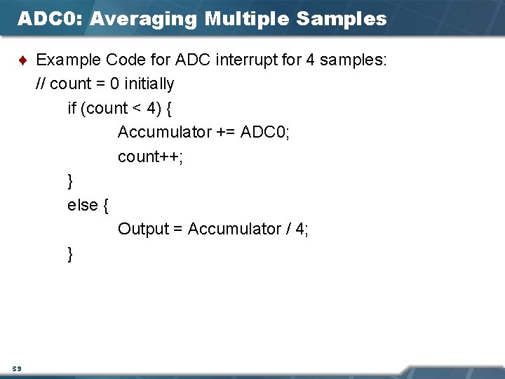
ADC: How to get rid of Noise ¨ If there is >1 LSB of noise in a system, averaging multiple samples together can yield a result with better noise resolution than the converter itself ¨ One way to do this is to set up an ADC interrupt which averages a certain number of samples before giving an output ¨ As mentioned earlier, just increasing the resolution of the ADC (number of bits) may not decrease the noise. 58

ADC 0: Averaging Multiple Samples ¨ Example Code for ADC interrupt for 4 samples: // count = 0 initially if (count < 4) { Accumulator += ADC 0; count++; } else { Output = Accumulator / 4; } 59

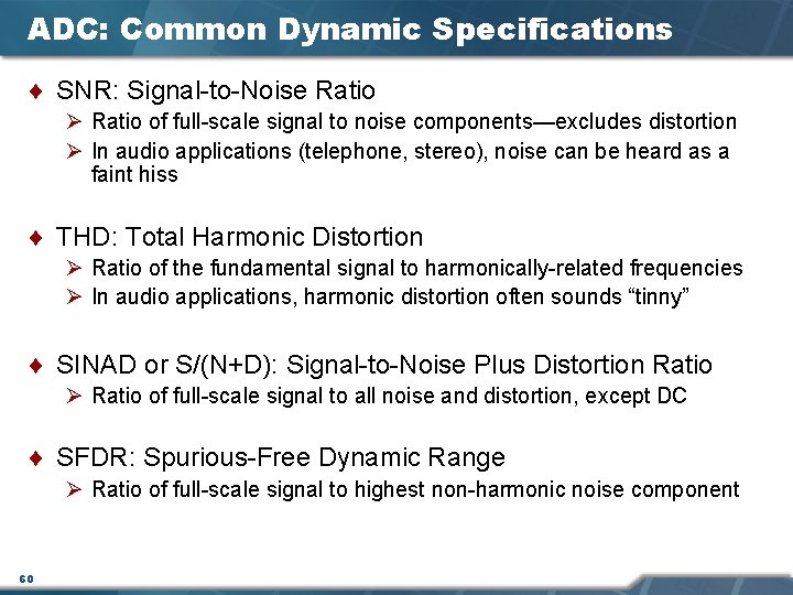
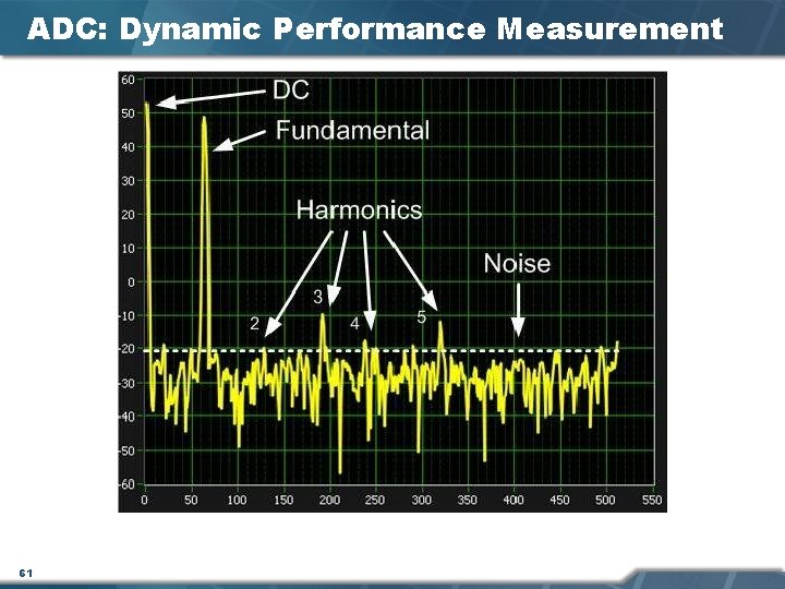
ADC: Common Dynamic Specifications ¨ SNR: Signal-to-Noise Ratio Ø Ratio of full-scale signal to noise components—excludes distortion Ø In audio applications (telephone, stereo), noise can be heard as a faint hiss ¨ THD: Total Harmonic Distortion Ø Ratio of the fundamental signal to harmonically-related frequencies Ø In audio applications, harmonic distortion often sounds “tinny” ¨ SINAD or S/(N+D): Signal-to-Noise Plus Distortion Ratio Ø Ratio of full-scale signal to all noise and distortion, except DC ¨ SFDR: Spurious-Free Dynamic Range Ø Ratio of full-scale signal to highest non-harmonic noise component 60

ADC: Dynamic Performance Measurement 61

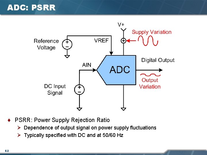
ADC: PSRR ¨ PSRR: Power Supply Rejection Ratio Ø Dependence of output signal on power supply fluctuations Ø Typically specified with DC and at 50/60 Hz 62

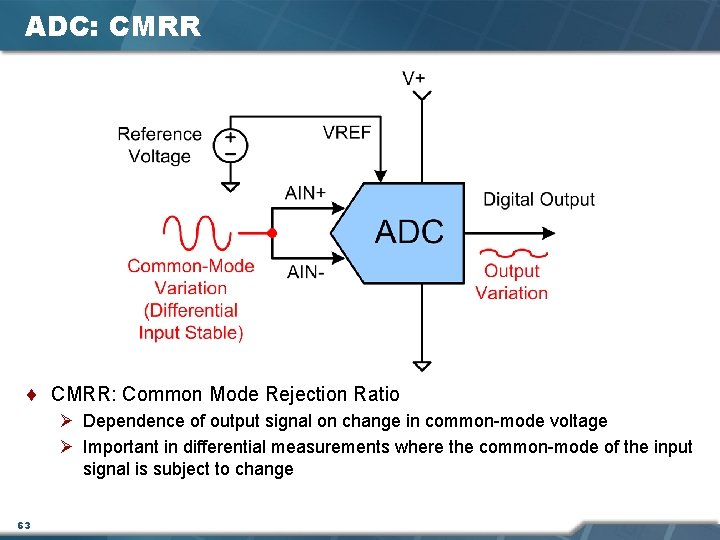
ADC: CMRR ¨ CMRR: Common Mode Rejection Ratio Ø Dependence of output signal on change in common-mode voltage Ø Important in differential measurements where the common-mode of the input signal is subject to change 63

IDAC Operation

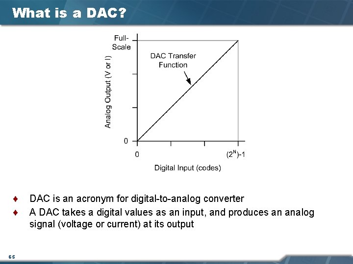
What is a DAC? ¨ ¨ 65 DAC is an acronym for digital-to-analog converter A DAC takes a digital values as an input, and produces an analog signal (voltage or current) at its output

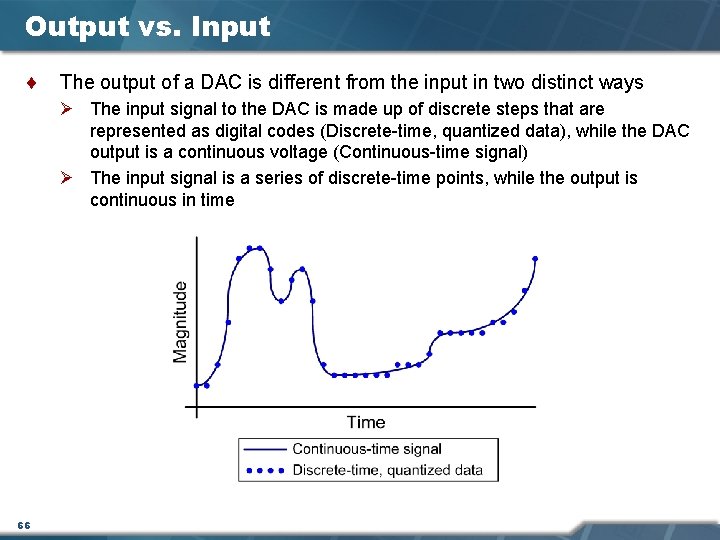
Output vs. Input ¨ The output of a DAC is different from the input in two distinct ways Ø The input signal to the DAC is made up of discrete steps that are represented as digital codes (Discrete-time, quantized data), while the DAC output is a continuous voltage (Continuous-time signal) Ø The input signal is a series of discrete-time points, while the output is continuous in time 66

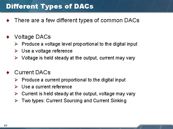
Different Types of DACs ¨ There a few different types of common DACs ¨ Voltage DACs Ø Produce a voltage level proportional to the digital input Ø Use a voltage reference Ø Voltage is held steady at the output, current may vary ¨ Current DACs Ø Ø 67 Produce a current proportional to the digital input Use a current reference Current is held steady at the output, voltage may vary Two types: Current Sourcing and Current Sinking

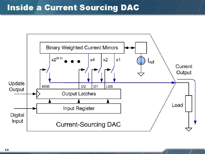
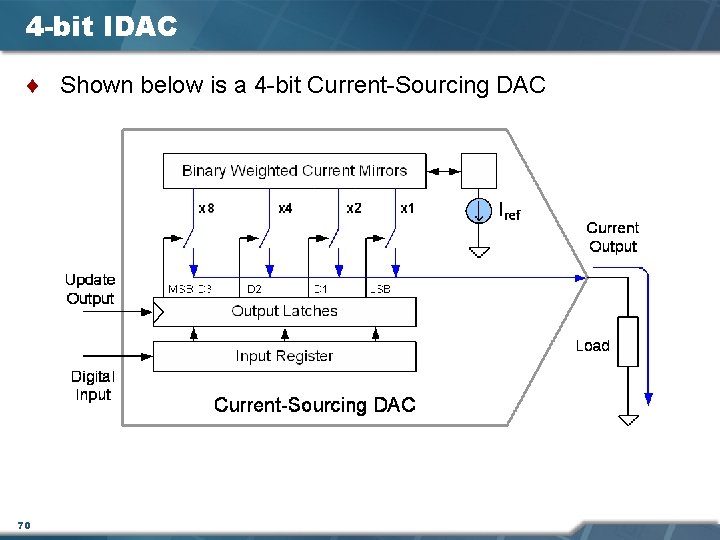
Inside a Current Sourcing DAC 68

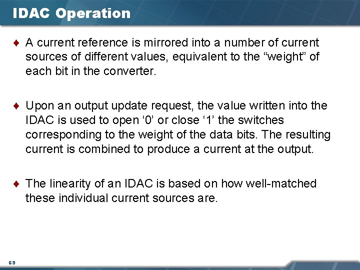
IDAC Operation ¨ A current reference is mirrored into a number of current sources of different values, equivalent to the “weight” of each bit in the converter. ¨ Upon an output update request, the value written into the IDAC is used to open ‘ 0’ or close ‘ 1’ the switches corresponding to the weight of the data bits. The resulting current is combined to produce a current at the output. ¨ The linearity of an IDAC is based on how well-matched these individual current sources are. 69

4 -bit IDAC ¨ Shown below is a 4 -bit Current-Sourcing DAC 70

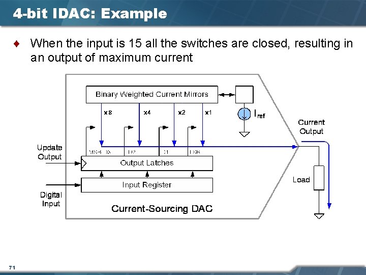
4 -bit IDAC: Example ¨ When the input is 15 all the switches are closed, resulting in an output of maximum current 71

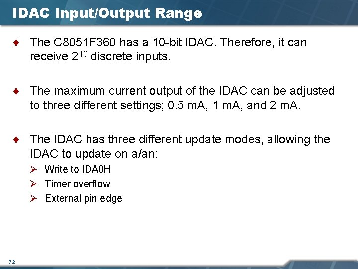
IDAC Input/Output Range ¨ The C 8051 F 360 has a 10 -bit IDAC. Therefore, it can receive 210 discrete inputs. ¨ The maximum current output of the IDAC can be adjusted to three different settings; 0. 5 m. A, 1 m. A, and 2 m. A. ¨ The IDAC has three different update modes, allowing the IDAC to update on a/an: Ø Write to IDA 0 H Ø Timer overflow Ø External pin edge 72
![IDAC Mode Details In its default mode IDA 0 CN 6 4 IDAC: Mode Details ¨ In its default mode (IDA 0 CN. [6: 4] =](https://slidetodoc.com/presentation_image_h/87ef0f9c2d67ce6cb16956b8a35b8196/image-73.jpg)
IDAC: Mode Details ¨ In its default mode (IDA 0 CN. [6: 4] = ‘ 111’), a write to IDA 0 H causes the IDAC to schedule an output update event. Note that a write to IDA 0 L will not cause the IDAC to update, hence, the write sequence should be IDA 0 L followed by IDA 0 H ¨ In timer overflow mode, the IDAC output updates when the timer overflows. Writes to the IDA 0 H and IDA 0 L registers are held until the timer overflows ¨ In external pin edge mode, writes to the IDAC data registers are held until and edge occurs on the CNVSTR input pin 73

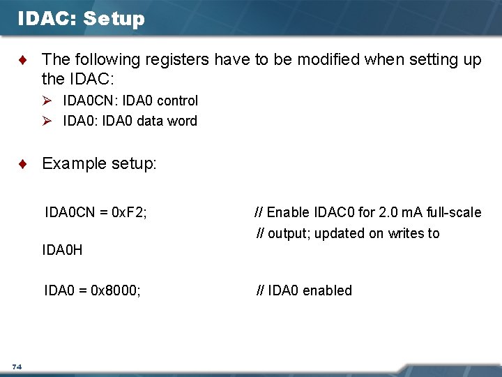
IDAC: Setup ¨ The following registers have to be modified when setting up the IDAC: Ø IDA 0 CN: IDA 0 control Ø IDA 0: IDA 0 data word ¨ Example setup: IDA 0 CN = 0 x. F 2; // Enable IDAC 0 for 2. 0 m. A full-scale // output; updated on writes to IDA 0 H IDA 0 = 0 x 8000; 74 // IDA 0 enabled

IDAC Performance Specifications

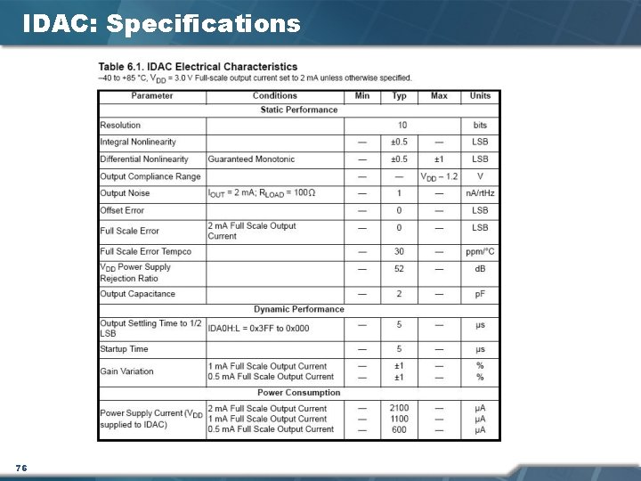
IDAC: Specifications 76

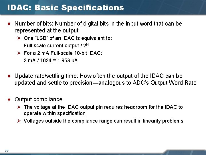
IDAC: Basic Specifications ¨ Number of bits: Number of digital bits in the input word that can be represented at the output Ø One “LSB” of an IDAC is equivalent to: Full-scale current output / 2 N Ø For a 2 m. A Full-scale 10 -bit IDAC: 2 m. A / 1024 = 1. 953 u. A ¨ Update rate/settling time: How often the output of the IDAC can be updated and settle to precision—analogous to ADC’s Output Word Rate ¨ Output compliance Ø The voltage at the IDAC output pin requires headroom for the IDAC to operate within specification Ø Voltages outside the compliance range can result in linearity problems 77

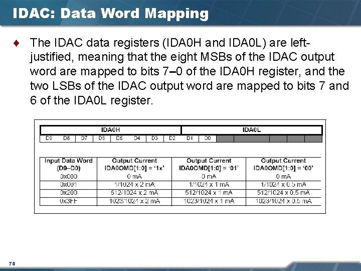
IDAC: Data Word Mapping ¨ The IDAC data registers (IDA 0 H and IDA 0 L) are leftjustified, meaning that the eight MSBs of the IDAC output word are mapped to bits 7– 0 of the IDA 0 H register, and the two LSBs of the IDAC output word are mapped to bits 7 and 6 of the IDA 0 L register. 78

IDAC: Additional Specifications ¨ DNL: Differential Nonlinearity ¨ INL: Integral Nonlinearity ¨ PSRR: Power Supply Rejection Ratio ¨ Much the same as the ADC specifications of the same names; refer to the ADC module for information on these topics 79

System-Level Error Compensation

System Error Sources ¨ In any system there a number of potential error sources ¨ The goal is to minimize the effects of errors which are relevant to the system 81

Calibration of System Offset and Slope ¨ Eliminating system-level offset and slope errors can be accomplished with digital calibration of the system at the output of the ADC ¨ If there are no significant linearity issues, the transfer function of the entire system can be determined using two known points on a line 82

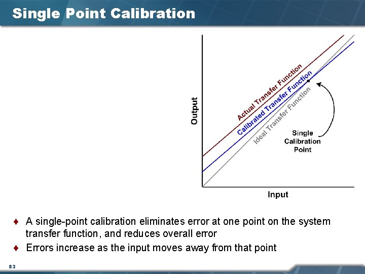
Single Point Calibration ¨ A single-point calibration eliminates error at one point on the system transfer function, and reduces overall error ¨ Errors increase as the input moves away from that point 83

Two Point Calibration ¨ A two-point calibration can eliminate offset and slope error across the entire system transfer function 84

Noise Reduction ¨ Noise in a system can be reduced using analog or digital filtering techniques. ¨ Simply averaging samples together will provide an efficient means of reducing the system noise. If the noise is white noise (Gaussian), averaging gives the most improvement. ¨ If noise is correlated, it can still be reduced drastically using averaging or other filter techniques, but it is best to find and eliminate the noise source. Ø Digital coupling into analog circuitry Ø Switching regulators 85

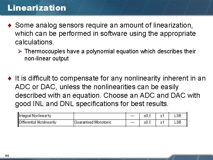
Linearization ¨ Some analog sensors require an amount of linearization, which can be performed in software using the appropriate calculations. Ø Thermocouples have a polynomial equation which describes their non-linear output ¨ It is difficult to compensate for any nonlinearity inherent in an ADC or DAC, unless the nonlinearities can be easily described with an equation. Choose an ADC and DAC with good INL and DNL specifications for best results. 86

www. silabs. com/MCU