Chapter 7 Complementary MOS CMOS Logic Design Microelectronic

- Slides: 54

Chapter 7 Complementary MOS (CMOS) Logic Design Microelectronic Circuit Design Richard C. Jaeger Travis N. Blalock Jaeger/Blalock 10/15/03 Microelectronic Circuit Design Mc. Graw-Hill 1

Chapter Goals • • • Introduce CMOS logic concepts Explore the voltage transfer characteristics CMOS inverters Learn to design basic and complex logic gates Discuss static and dynamic power in CMOS logic Present expressions for dynamic performance of CMOS logic devices Present noise margins for CMOS logic Introduce dynamic logic and domino CMOS logic techniques Introduce design techniques for “cascade buffers” Explore layout of CMOS logic gates Discuss the concept of “latchup” Jaeger/Blalock 10/15/03 Microelectronic Circuit Design Mc. Graw-Hill 2

CMOS Inverter Technology • Complementary MOS, or CMOS, needs both PMOS and NMOS devices for their logic gates to be realized • The concept of CMOS was introduced in 1963 by Wanlass and Sah, but it did not become common until the 1980’s as NMOS microprocessors were dissipating as much as 50 W and alternative design technique was needed • CMOS still dominates digital IC design today Jaeger/Blalock 10/15/03 Microelectronic Circuit Design Mc. Graw-Hill 3

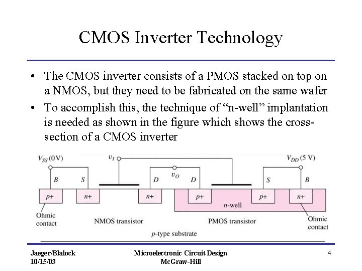
CMOS Inverter Technology • The CMOS inverter consists of a PMOS stacked on top on a NMOS, but they need to be fabricated on the same wafer • To accomplish this, the technique of “n-well” implantation is needed as shown in the figure which shows the crosssection of a CMOS inverter Jaeger/Blalock 10/15/03 Microelectronic Circuit Design Mc. Graw-Hill 4

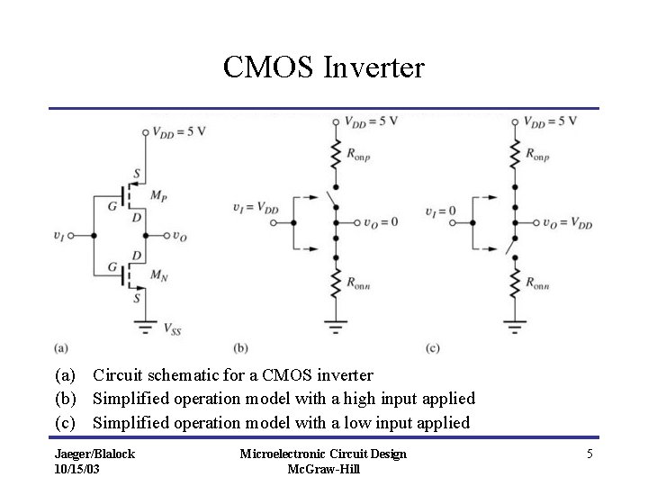
CMOS Inverter (a) Circuit schematic for a CMOS inverter (b) Simplified operation model with a high input applied (c) Simplified operation model with a low input applied Jaeger/Blalock 10/15/03 Microelectronic Circuit Design Mc. Graw-Hill 5

CMOS Inverter Operation • When v. I is pulled high (VDD), the PMOS inverter is turned off, while the NMOS is turned on pulling the output down to VSS • When v. I is pulled low (VSS), the NMOS inverter is turned off, while the PMOS is turned on pulling the output up to VDD Jaeger/Blalock 10/15/03 Microelectronic Circuit Design Mc. Graw-Hill 6

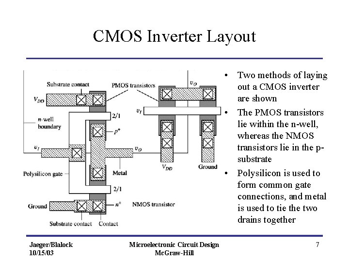
CMOS Inverter Layout • Two methods of laying out a CMOS inverter are shown • The PMOS transistors lie within the n-well, whereas the NMOS transistors lie in the psubstrate • Polysilicon is used to form common gate connections, and metal is used to tie the two drains together Jaeger/Blalock 10/15/03 Microelectronic Circuit Design Mc. Graw-Hill 7

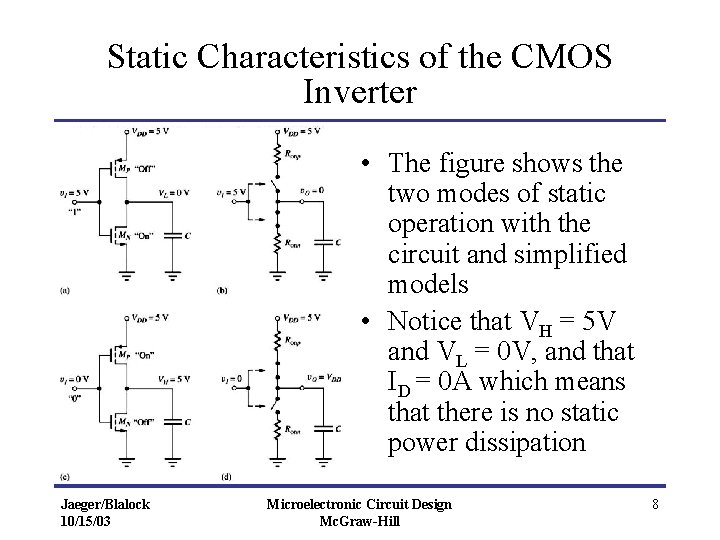
Static Characteristics of the CMOS Inverter • The figure shows the two modes of static operation with the circuit and simplified models • Notice that VH = 5 V and VL = 0 V, and that ID = 0 A which means that there is no static power dissipation Jaeger/Blalock 10/15/03 Microelectronic Circuit Design Mc. Graw-Hill 8

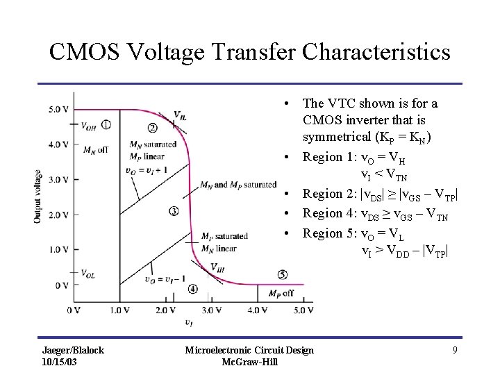
CMOS Voltage Transfer Characteristics • The VTC shown is for a CMOS inverter that is symmetrical (KP = KN) • Region 1: v. O = VH v. I < VTN • Region 2: |v. DS| ≥ |v. GS – VTP| • Region 4: v. DS ≥ v. GS – VTN • Region 5: v. O = VL v. I > VDD – |VTP| Jaeger/Blalock 10/15/03 Microelectronic Circuit Design Mc. Graw-Hill 9

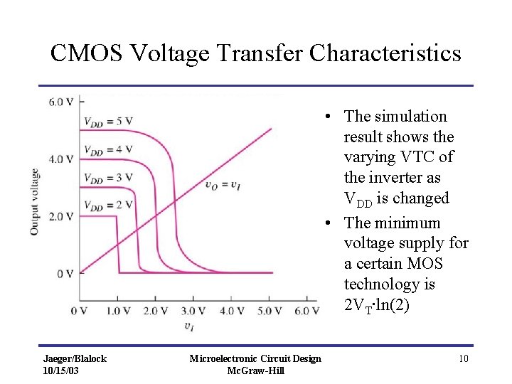
CMOS Voltage Transfer Characteristics • The simulation result shows the varying VTC of the inverter as VDD is changed • The minimum voltage supply for a certain MOS technology is 2 VT∙ln(2) Jaeger/Blalock 10/15/03 Microelectronic Circuit Design Mc. Graw-Hill 10

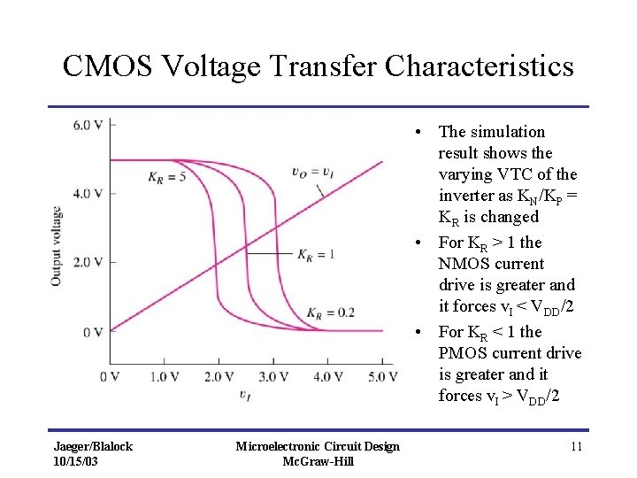
CMOS Voltage Transfer Characteristics • The simulation result shows the varying VTC of the inverter as KN/KP = KR is changed • For KR > 1 the NMOS current drive is greater and it forces v. I < VDD/2 • For KR < 1 the PMOS current drive is greater and it forces v. I > VDD/2 Jaeger/Blalock 10/15/03 Microelectronic Circuit Design Mc. Graw-Hill 11

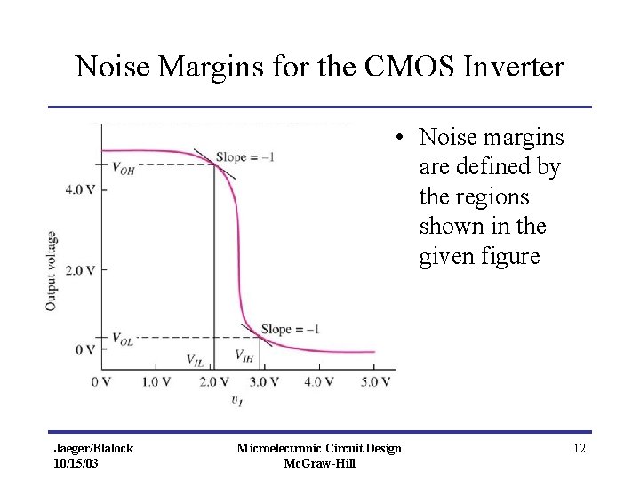
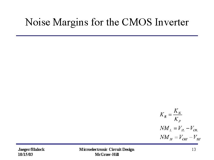
Noise Margins for the CMOS Inverter • Noise margins are defined by the regions shown in the given figure Jaeger/Blalock 10/15/03 Microelectronic Circuit Design Mc. Graw-Hill 12

Noise Margins for the CMOS Inverter Jaeger/Blalock 10/15/03 Microelectronic Circuit Design Mc. Graw-Hill 13

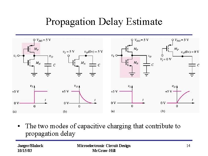
Propagation Delay Estimate • The two modes of capacitive charging that contribute to propagation delay Jaeger/Blalock 10/15/03 Microelectronic Circuit Design Mc. Graw-Hill 14

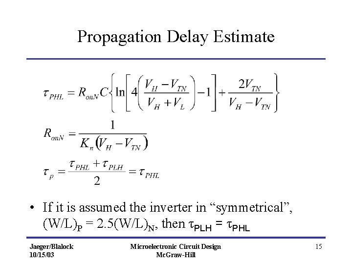
Propagation Delay Estimate • If it is assumed the inverter in “symmetrical”, (W/L)P = 2. 5(W/L)N, then τPLH = τPHL Jaeger/Blalock 10/15/03 Microelectronic Circuit Design Mc. Graw-Hill 15

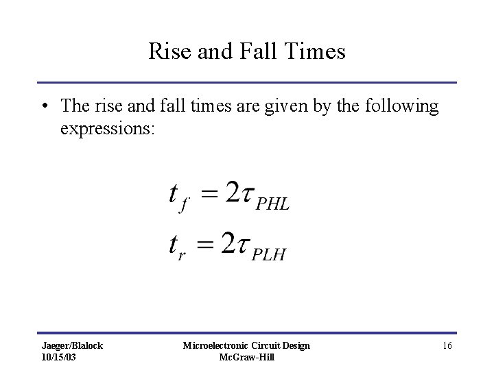
Rise and Fall Times • The rise and fall times are given by the following expressions: Jaeger/Blalock 10/15/03 Microelectronic Circuit Design Mc. Graw-Hill 16

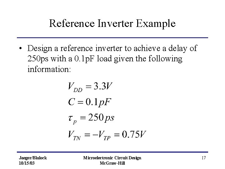
Reference Inverter Example • Design a reference inverter to achieve a delay of 250 ps with a 0. 1 p. F load given the following information: Jaeger/Blalock 10/15/03 Microelectronic Circuit Design Mc. Graw-Hill 17

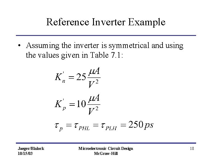
Reference Inverter Example • Assuming the inverter is symmetrical and using the values given in Table 7. 1: Jaeger/Blalock 10/15/03 Microelectronic Circuit Design Mc. Graw-Hill 18

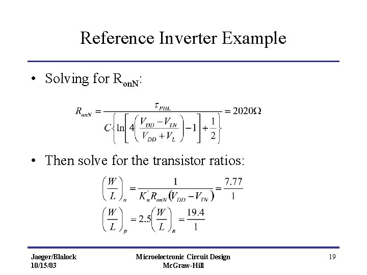
Reference Inverter Example • Solving for Ron. N: • Then solve for the transistor ratios: Jaeger/Blalock 10/15/03 Microelectronic Circuit Design Mc. Graw-Hill 19

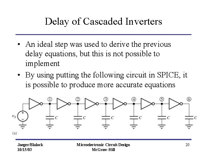
Delay of Cascaded Inverters • An ideal step was used to derive the previous delay equations, but this is not possible to implement • By using putting the following circuit in SPICE, it is possible to produce more accurate equations Jaeger/Blalock 10/15/03 Microelectronic Circuit Design Mc. Graw-Hill 20

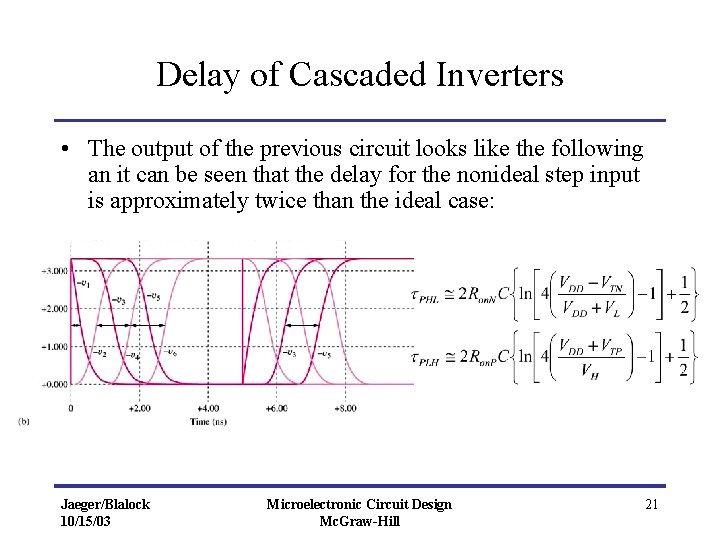
Delay of Cascaded Inverters • The output of the previous circuit looks like the following an it can be seen that the delay for the nonideal step input is approximately twice than the ideal case: Jaeger/Blalock 10/15/03 Microelectronic Circuit Design Mc. Graw-Hill 21

Static Power Dissipation • CMOS logic is considered to have no static power dissipation • Since the ROFF of the two transistors is very large, the DC current driving a capacitive load is zero • This is not completely accurate since MOS transistors have leakage currents associated with the reverse-biased drain-to-substrate connections Jaeger/Blalock 10/15/03 Microelectronic Circuit Design Mc. Graw-Hill 22

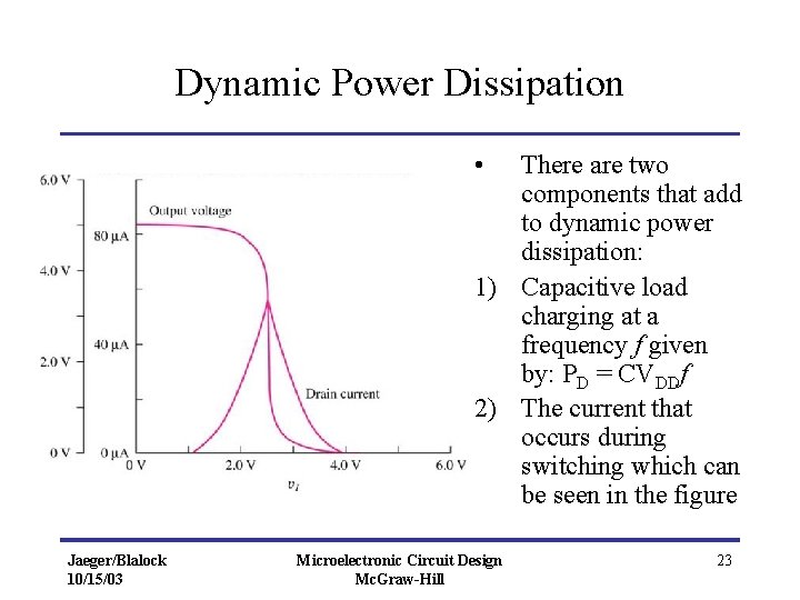
Dynamic Power Dissipation • There are two components that add to dynamic power dissipation: 1) Capacitive load charging at a frequency f given by: PD = CVDDf 2) The current that occurs during switching which can be seen in the figure Jaeger/Blalock 10/15/03 Microelectronic Circuit Design Mc. Graw-Hill 23

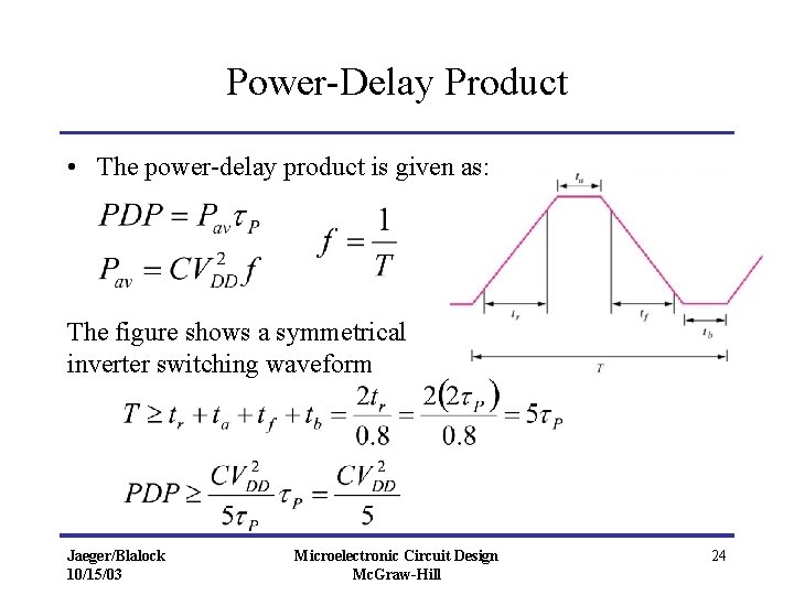
Power-Delay Product • The power-delay product is given as: The figure shows a symmetrical inverter switching waveform Jaeger/Blalock 10/15/03 Microelectronic Circuit Design Mc. Graw-Hill 24

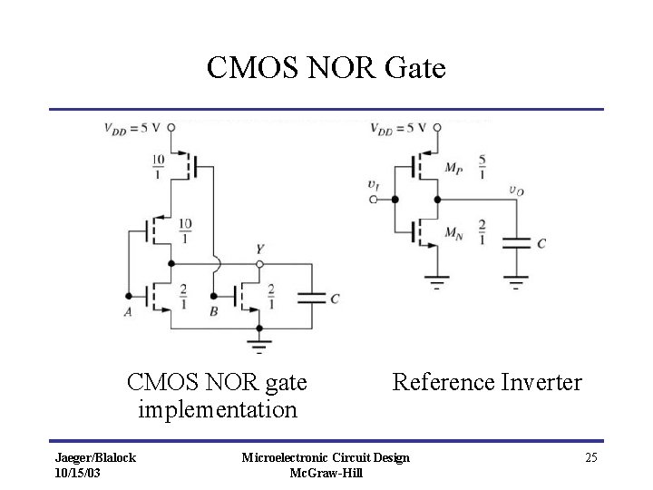
CMOS NOR Gate CMOS NOR gate implementation Jaeger/Blalock 10/15/03 Reference Inverter Microelectronic Circuit Design Mc. Graw-Hill 25

CMOS NOR Gate Sizing • When sizing the transistors, it is ideal to keep the delay times the same as the reference inverter • To accomplish this, the on-resistance on the PMOS branch of the NOR gate must be the same as the reference inverter • For a two-input NOR gate, the (W/L)p must be made twice as large Jaeger/Blalock 10/15/03 Microelectronic Circuit Design Mc. Graw-Hill 26

CMOS NOR Gate Body Effect • Since the bottom PMOS body contact is not connected to its source, its threshold voltage changes as VSB changes during switching • Once v. O = VH is reached, the bottom PMOS is not affected by body effect, thus the total on-resistance of the PMOS branch is the same • However, the rise time is slowed down due to |VTP| being a function of time Jaeger/Blalock 10/15/03 Microelectronic Circuit Design Mc. Graw-Hill 27

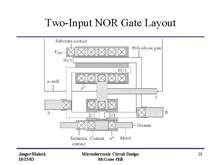
Two-Input NOR Gate Layout Jaeger/Blalock 10/15/03 Microelectronic Circuit Design Mc. Graw-Hill 28

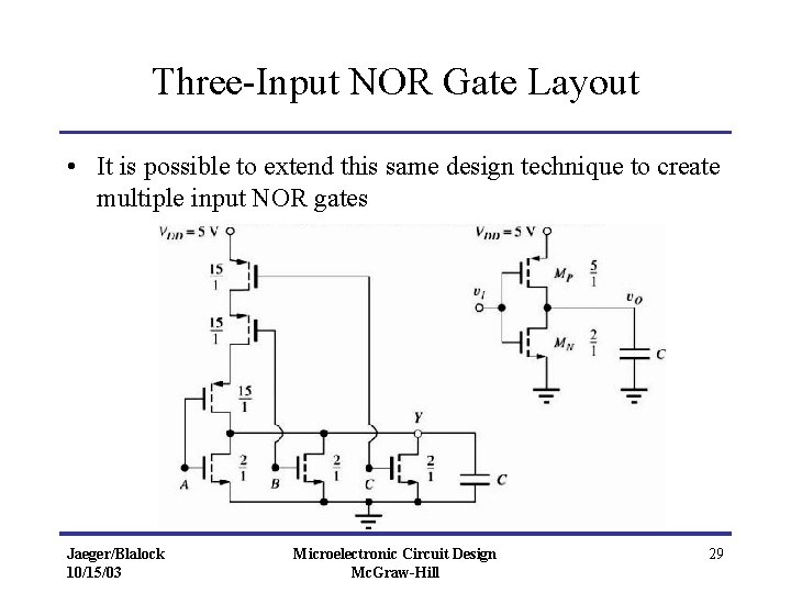
Three-Input NOR Gate Layout • It is possible to extend this same design technique to create multiple input NOR gates Jaeger/Blalock 10/15/03 Microelectronic Circuit Design Mc. Graw-Hill 29

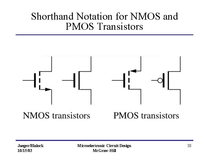
Shorthand Notation for NMOS and PMOS Transistors Jaeger/Blalock 10/15/03 Microelectronic Circuit Design Mc. Graw-Hill 30

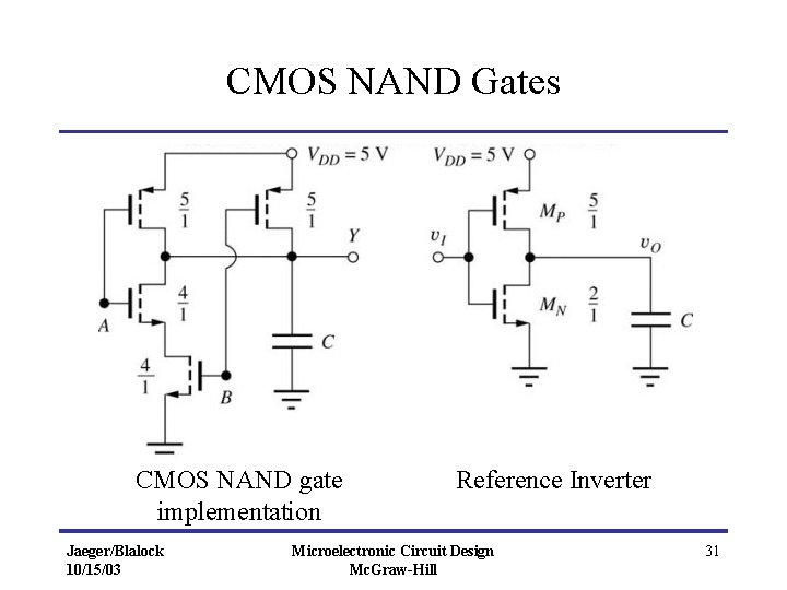
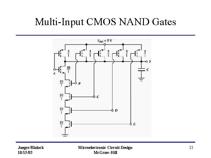
CMOS NAND Gates CMOS NAND gate implementation Jaeger/Blalock 10/15/03 Reference Inverter Microelectronic Circuit Design Mc. Graw-Hill 31

CMOS NAND Gates Sizing • The same rules apply for sizing the NAND gate as the did for the NOR gate, except for now the NMOS transistors are in series • The (W/L)N will be twice the size of the reference inverter’s NMOS Jaeger/Blalock 10/15/03 Microelectronic Circuit Design Mc. Graw-Hill 32

Multi-Input CMOS NAND Gates Jaeger/Blalock 10/15/03 Microelectronic Circuit Design Mc. Graw-Hill 33

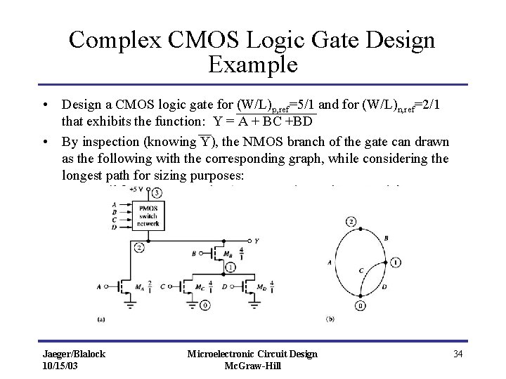
Complex CMOS Logic Gate Design Example • Design a CMOS logic gate for (W/L)p, ref=5/1 and for (W/L)n, ref=2/1 that exhibits the function: Y = A + BC +BD • By inspection (knowing Y), the NMOS branch of the gate can drawn as the following with the corresponding graph, while considering the longest path for sizing purposes: Jaeger/Blalock 10/15/03 Microelectronic Circuit Design Mc. Graw-Hill 34

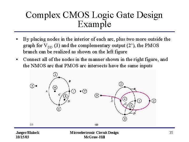
Complex CMOS Logic Gate Design Example • By placing nodes in the interior of each arc, plus two more outside the graph for VDD (3) and the complementary output (2’), the PMOS branch can be realized as shown on the left figure • Connect all of the nodes in the manner shown in the right figure, and the NMOS arc that PMOS arc intersects have the same inputs Jaeger/Blalock 10/15/03 Microelectronic Circuit Design Mc. Graw-Hill 35

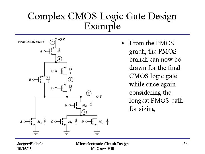
Complex CMOS Logic Gate Design Example • From the PMOS graph, the PMOS branch can now be drawn for the final CMOS logic gate while once again considering the longest PMOS path for sizing Jaeger/Blalock 10/15/03 Microelectronic Circuit Design Mc. Graw-Hill 36

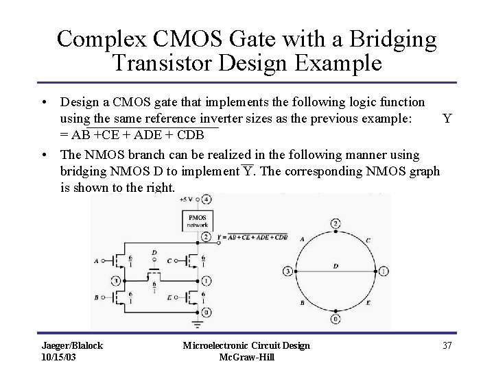
Complex CMOS Gate with a Bridging Transistor Design Example • Design a CMOS gate that implements the following logic function using the same reference inverter sizes as the previous example: Y = AB +CE + ADE + CDB • The NMOS branch can be realized in the following manner using bridging NMOS D to implement Y. The corresponding NMOS graph is shown to the right. Jaeger/Blalock 10/15/03 Microelectronic Circuit Design Mc. Graw-Hill 37

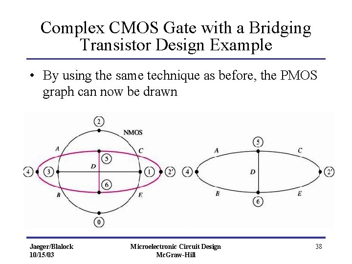
Complex CMOS Gate with a Bridging Transistor Design Example • By using the same technique as before, the PMOS graph can now be drawn Jaeger/Blalock 10/15/03 Microelectronic Circuit Design Mc. Graw-Hill 38

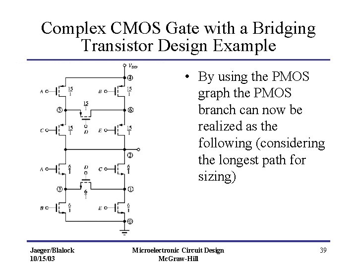
Complex CMOS Gate with a Bridging Transistor Design Example • By using the PMOS graph the PMOS branch can now be realized as the following (considering the longest path for sizing) Jaeger/Blalock 10/15/03 Microelectronic Circuit Design Mc. Graw-Hill 39

Minimum Size Gate Design and Performance • With CMOS technology, there is a area/delay tradeoff that needs to be considered • If minimum feature sized are used for both devices, then the τPLH will be decreased compared to the symmetrical reference inverter Jaeger/Blalock 10/15/03 Microelectronic Circuit Design Mc. Graw-Hill 40

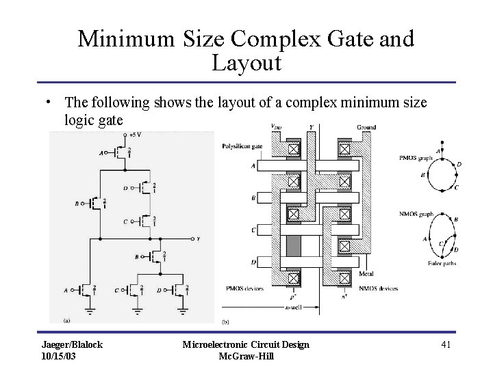
Minimum Size Complex Gate and Layout • The following shows the layout of a complex minimum size logic gate Jaeger/Blalock 10/15/03 Microelectronic Circuit Design Mc. Graw-Hill 41

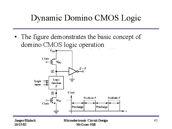
Dynamic Domino CMOS Logic • One technique to help decrease power in MOS logic circuits is dynamic logic • Dynamic logic uses different precharge and evaluation phases that are controlled by a system clock to eliminate the dc current path in single channel logic circuits • Early MOS logic required multiphase clocks to accomplish this, but CMOS logic can be operated dynamically with a single clock Jaeger/Blalock 10/15/03 Microelectronic Circuit Design Mc. Graw-Hill 42

Dynamic Domino CMOS Logic • The figure demonstrates the basic concept of domino CMOS logic operation Jaeger/Blalock 10/15/03 Microelectronic Circuit Design Mc. Graw-Hill 43

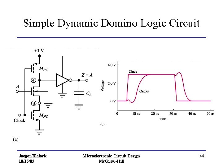
Simple Dynamic Domino Logic Circuit Jaeger/Blalock 10/15/03 Microelectronic Circuit Design Mc. Graw-Hill 44

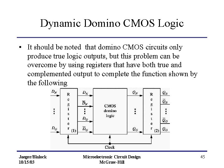
Dynamic Domino CMOS Logic • It should be noted that domino CMOS circuits only produce true logic outputs, but this problem can be overcome by using registers that have both true and complemented output to complete the function shown by the following Jaeger/Blalock 10/15/03 Microelectronic Circuit Design Mc. Graw-Hill 45

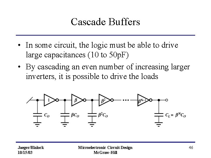
Cascade Buffers • In some circuit, the logic must be able to drive large capacitances (10 to 50 p. F) • By cascading an even number of increasing larger inverters, it is possible to drive the loads Jaeger/Blalock 10/15/03 Microelectronic Circuit Design Mc. Graw-Hill 46

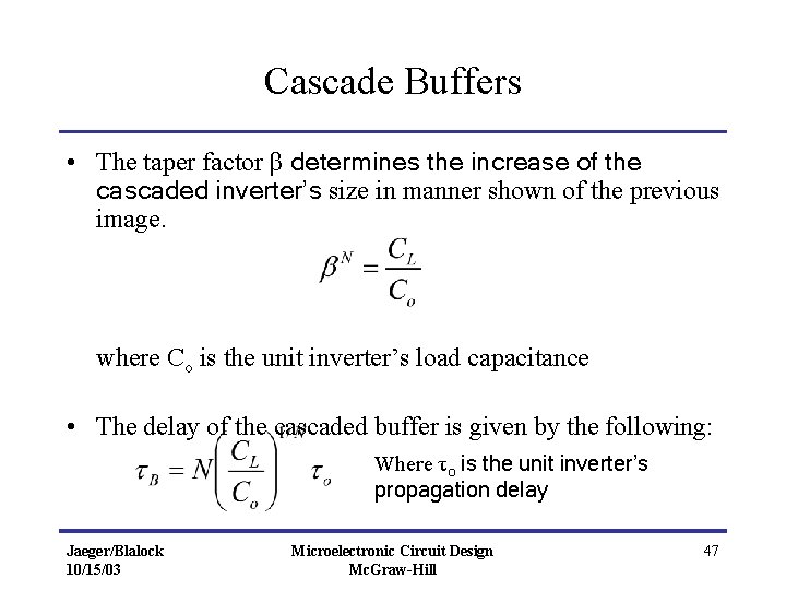
Cascade Buffers • The taper factor β determines the increase of the cascaded inverter’s size in manner shown of the previous image. where Co is the unit inverter’s load capacitance • The delay of the cascaded buffer is given by the following: Where τo is the unit inverter’s propagation delay Jaeger/Blalock 10/15/03 Microelectronic Circuit Design Mc. Graw-Hill 47

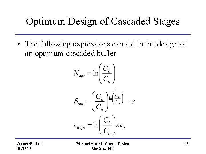
Optimum Design of Cascaded Stages • The following expressions can aid in the design of an optimum cascaded buffer Jaeger/Blalock 10/15/03 Microelectronic Circuit Design Mc. Graw-Hill 48

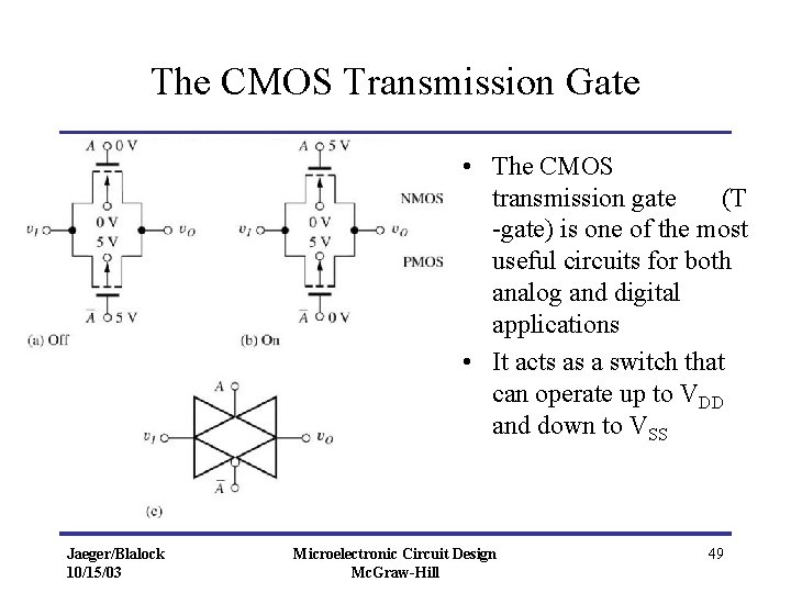
The CMOS Transmission Gate • The CMOS transmission gate (T -gate) is one of the most useful circuits for both analog and digital applications • It acts as a switch that can operate up to VDD and down to VSS Jaeger/Blalock 10/15/03 Microelectronic Circuit Design Mc. Graw-Hill 49

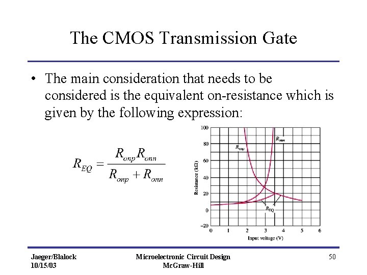
The CMOS Transmission Gate • The main consideration that needs to be considered is the equivalent on-resistance which is given by the following expression: Jaeger/Blalock 10/15/03 Microelectronic Circuit Design Mc. Graw-Hill 50

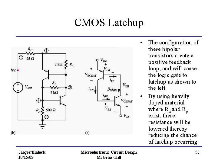
CMOS Latchup • There is one major downfall to the CMOS logic gate – Latchup • There are many safeguards that are done during fabrication to suppress this, but it can still occur under certain transient or fault conditions Jaeger/Blalock 10/15/03 Microelectronic Circuit Design Mc. Graw-Hill 51

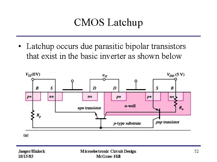
CMOS Latchup • Latchup occurs due parasitic bipolar transistors that exist in the basic inverter as shown below Jaeger/Blalock 10/15/03 Microelectronic Circuit Design Mc. Graw-Hill 52

CMOS Latchup • The configuration of these bipolar transistors create a positive feedback loop, and will cause the logic gate to latchup as shown to the left • By using heavily doped material where Rn and Rp exist, there resistance will be lowered thereby reducing the chance of latchup occurring Jaeger/Blalock 10/15/03 Microelectronic Circuit Design Mc. Graw-Hill 53

End of Chapter 7 Jaeger/Blalock 10/15/03 Microelectronic Circuit Design Mc. Graw-Hill 54