CHAPTER 5 MOS FieldEffect Transistors MOSFETs Microelectronic Circuits
- Slides: 110

CHAPTER 5 MOS Field-Effect Transistors (MOSFETs) Microelectronic Circuits, Sixth Edition Sedra/Smith Copyright © 2010 by Oxford University Press, Inc.

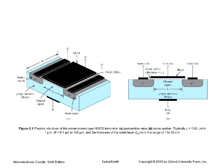
Microelectronic Circuits, Sixth Edition Sedra/Smith Copyright © 2010 by Oxford University Press, Inc.

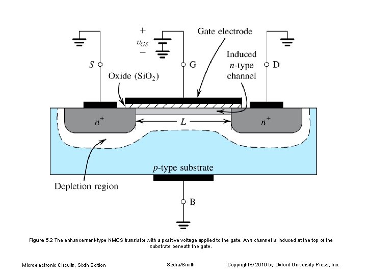
Figure 5. 2 The enhancement-type NMOS transistor with a positive voltage applied to the gate. An n channel is induced at the top of the substrate beneath the gate. Microelectronic Circuits, Sixth Edition Sedra/Smith Copyright © 2010 by Oxford University Press, Inc.

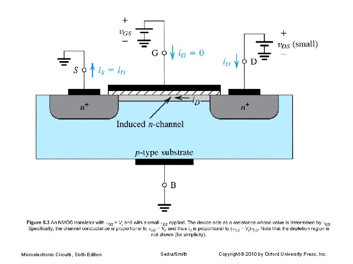
Microelectronic Circuits, Sixth Edition Sedra/Smith Copyright © 2010 by Oxford University Press, Inc.

Microelectronic Circuits, Sixth Edition Sedra/Smith Copyright © 2010 by Oxford University Press, Inc.

Microelectronic Circuits, Sixth Edition Sedra/Smith Copyright © 2010 by Oxford University Press, Inc.

Microelectronic Circuits, Sixth Edition Sedra/Smith Copyright © 2010 by Oxford University Press, Inc.

Microelectronic Circuits, Sixth Edition Sedra/Smith Copyright © 2010 by Oxford University Press, Inc.

Microelectronic Circuits, Sixth Edition Sedra/Smith Copyright © 2010 by Oxford University Press, Inc.

Microelectronic Circuits, Sixth Edition Sedra/Smith Copyright © 2010 by Oxford University Press, Inc.

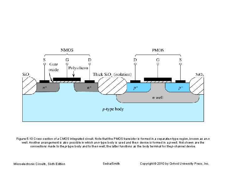
Figure 5. 10 Cross-section of a CMOS integrated circuit. Note that the PMOS transistor is formed in a separate n-type region, known as an n well. Another arrangement is also possible in which an n-type body is used and the n device is formed in a p well. Not shown are the connections made to the p-type body and to the n well; the latter functions as the body terminal for the p-channel device. Microelectronic Circuits, Sixth Edition Sedra/Smith Copyright © 2010 by Oxford University Press, Inc.

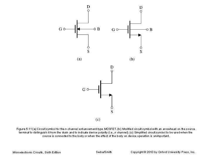
Figure 5. 11 (a) Circuit symbol for the n-channel enhancement-type MOSFET. (b) Modified circuit symbol with an arrowhead on the source terminal to distinguish it from the drain and to indicate device polarity (i. e. , n channel). (c) Simplified circuit symbol to be used when the source is connected to the body or when the effect of the body on device operation is unimportant. Microelectronic Circuits, Sixth Edition Sedra/Smith Copyright © 2010 by Oxford University Press, Inc.

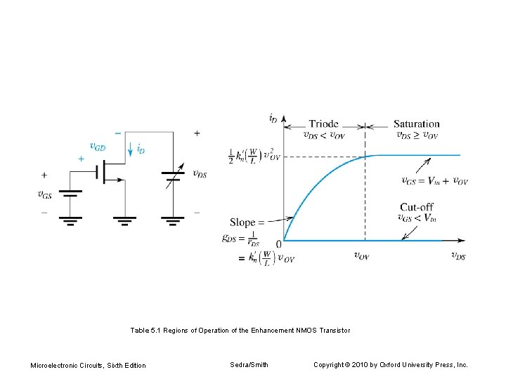
Table 5. 1 Regions of Operation of the Enhancement NMOS Transistor Microelectronic Circuits, Sixth Edition Sedra/Smith Copyright © 2010 by Oxford University Press, Inc.

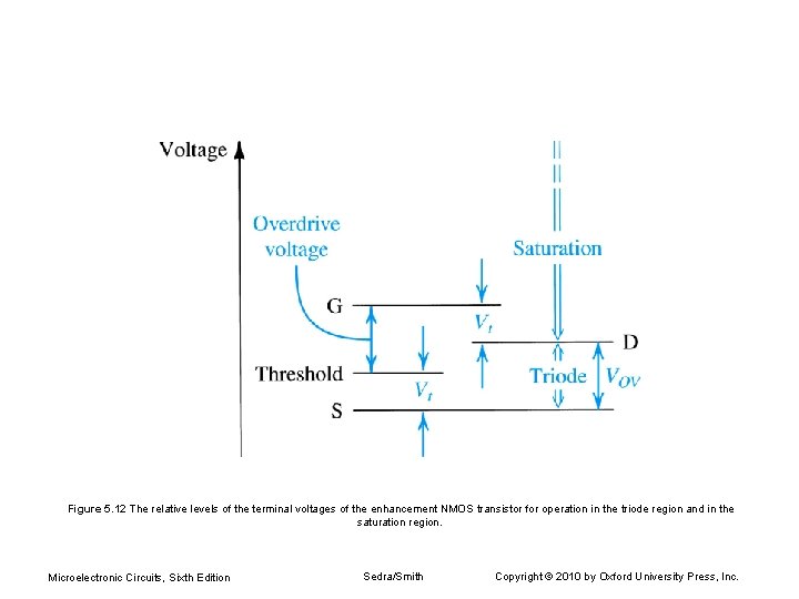
Figure 5. 12 The relative levels of the terminal voltages of the enhancement NMOS transistor for operation in the triode region and in the saturation region. Microelectronic Circuits, Sixth Edition Sedra/Smith Copyright © 2010 by Oxford University Press, Inc.

Microelectronic Circuits, Sixth Edition Sedra/Smith Copyright © 2010 by Oxford University Press, Inc.

Microelectronic Circuits, Sixth Edition Sedra/Smith Copyright © 2010 by Oxford University Press, Inc.

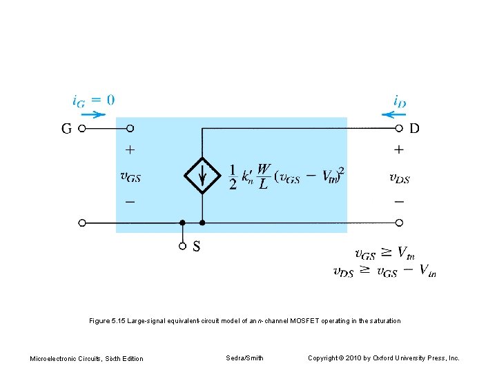
Figure 5. 15 Large-signal equivalent-circuit model of an n-channel MOSFET operating in the saturation Microelectronic Circuits, Sixth Edition Sedra/Smith Copyright © 2010 by Oxford University Press, Inc.

Microelectronic Circuits, Sixth Edition Sedra/Smith Copyright © 2010 by Oxford University Press, Inc.

Microelectronic Circuits, Sixth Edition Sedra/Smith Copyright © 2010 by Oxford University Press, Inc.

Microelectronic Circuits, Sixth Edition Sedra/Smith Copyright © 2010 by Oxford University Press, Inc.

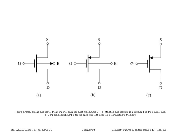
Figure 5. 19 (a) Circuit symbol for the p-channel enhancement-type MOSFET. (b) Modified symbol with an arrowhead on the source lead. (c) Simplified circuit symbol for the case where the source is connected to the body. Microelectronic Circuits, Sixth Edition Sedra/Smith Copyright © 2010 by Oxford University Press, Inc.

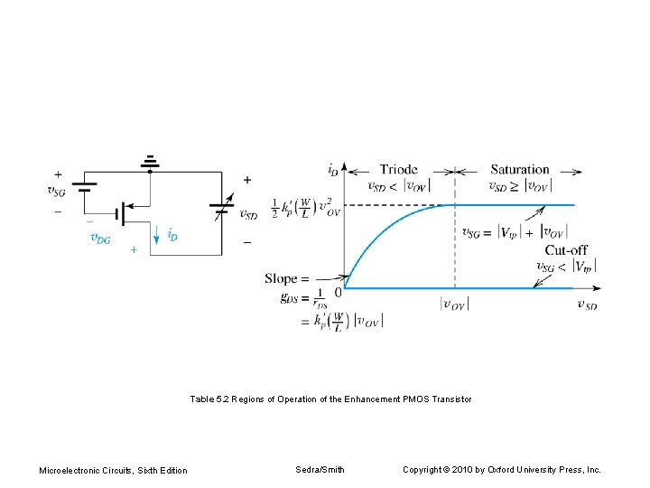
Table 5. 2 Regions of Operation of the Enhancement PMOS Transistor Microelectronic Circuits, Sixth Edition Sedra/Smith Copyright © 2010 by Oxford University Press, Inc.

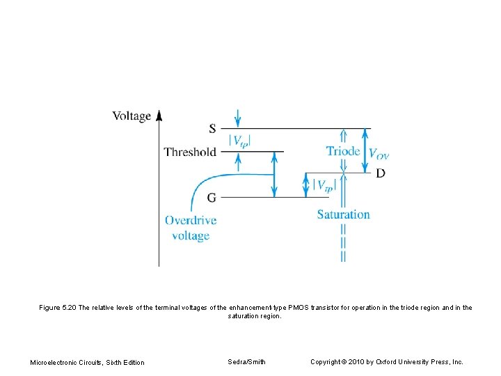
Figure 5. 20 The relative levels of the terminal voltages of the enhancement-type PMOS transistor for operation in the triode region and in the saturation region. Microelectronic Circuits, Sixth Edition Sedra/Smith Copyright © 2010 by Oxford University Press, Inc.

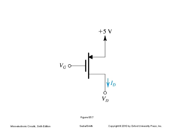
Figure E 5. 7 Microelectronic Circuits, Sixth Edition Sedra/Smith Copyright © 2010 by Oxford University Press, Inc.

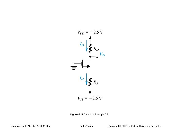
Figure 5. 21 Circuit for Example 5. 3. Microelectronic Circuits, Sixth Edition Sedra/Smith Copyright © 2010 by Oxford University Press, Inc.

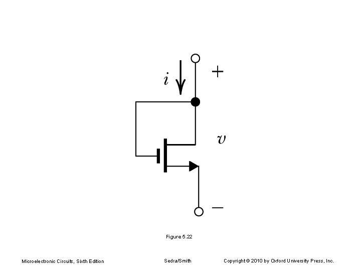
Figure 5. 22 Microelectronic Circuits, Sixth Edition Sedra/Smith Copyright © 2010 by Oxford University Press, Inc.

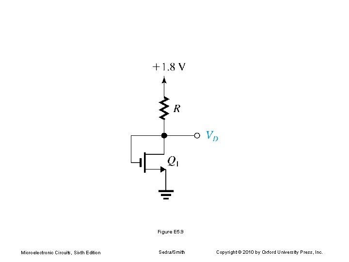
Figure E 5. 9 Microelectronic Circuits, Sixth Edition Sedra/Smith Copyright © 2010 by Oxford University Press, Inc.

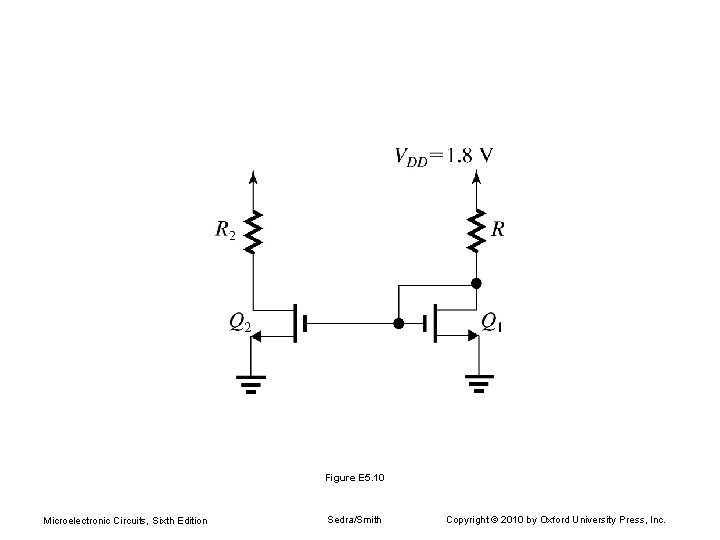
Figure E 5. 10 Microelectronic Circuits, Sixth Edition Sedra/Smith Copyright © 2010 by Oxford University Press, Inc.

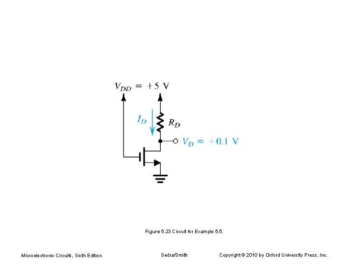
Figure 5. 23 Circuit for Example 5. 5. Microelectronic Circuits, Sixth Edition Sedra/Smith Copyright © 2010 by Oxford University Press, Inc.

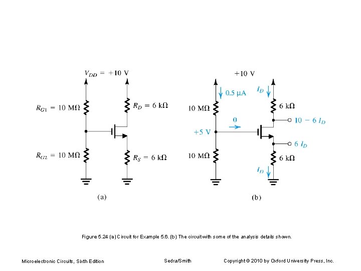
Figure 5. 24 (a) Circuit for Example 5. 6. (b) The circuit with some of the analysis details shown. Microelectronic Circuits, Sixth Edition Sedra/Smith Copyright © 2010 by Oxford University Press, Inc.

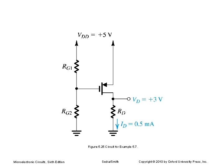
Figure 5. 25 Circuit for Example 5. 7. Microelectronic Circuits, Sixth Edition Sedra/Smith Copyright © 2010 by Oxford University Press, Inc.

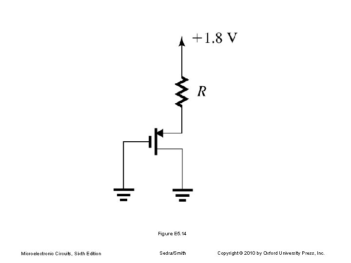
Figure E 5. 14 Microelectronic Circuits, Sixth Edition Sedra/Smith Copyright © 2010 by Oxford University Press, Inc.

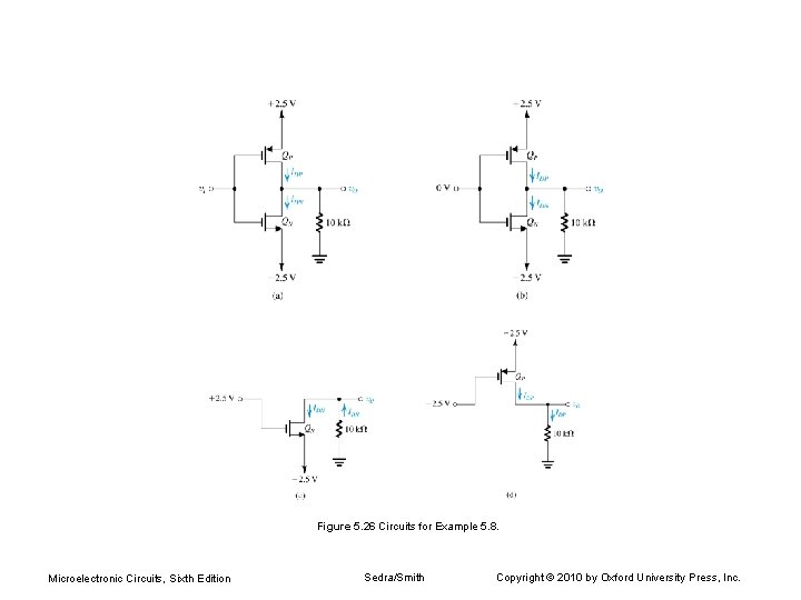
Figure 5. 26 Circuits for Example 5. 8. Microelectronic Circuits, Sixth Edition Sedra/Smith Copyright © 2010 by Oxford University Press, Inc.

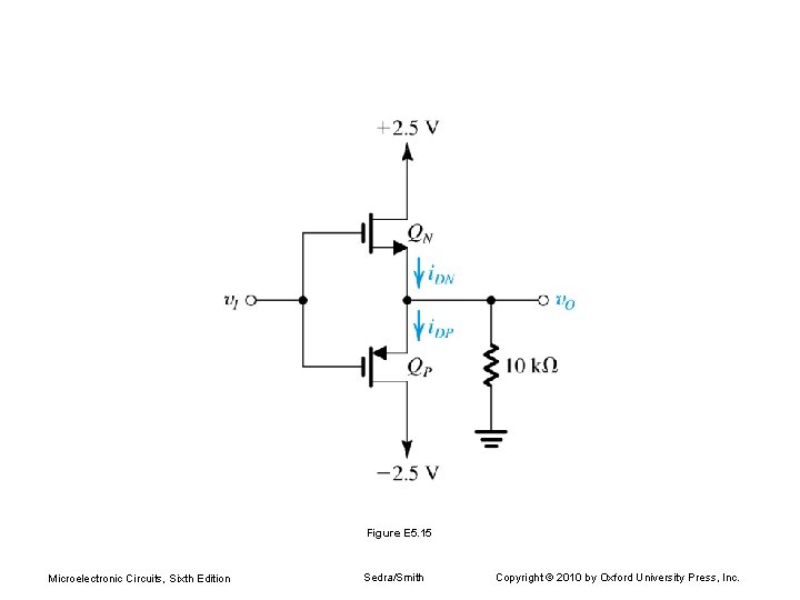
Figure E 5. 15 Microelectronic Circuits, Sixth Edition Sedra/Smith Copyright © 2010 by Oxford University Press, Inc.

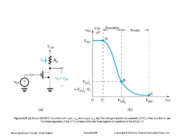
Microelectronic Circuits, Sixth Edition Sedra/Smith Copyright © 2010 by Oxford University Press, Inc.

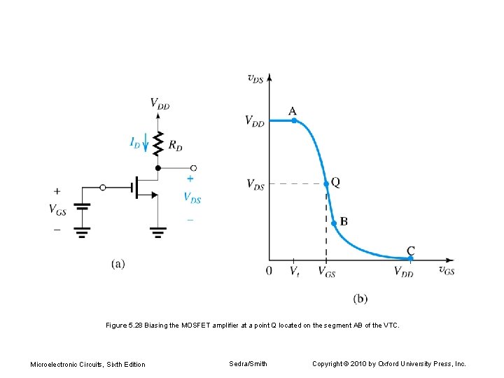
Figure 5. 28 Biasing the MOSFET amplifier at a point Q located on the segment AB of the VTC. Microelectronic Circuits, Sixth Edition Sedra/Smith Copyright © 2010 by Oxford University Press, Inc.

Microelectronic Circuits, Sixth Edition Sedra/Smith Copyright © 2010 by Oxford University Press, Inc.

Microelectronic Circuits, Sixth Edition Sedra/Smith Copyright © 2010 by Oxford University Press, Inc.

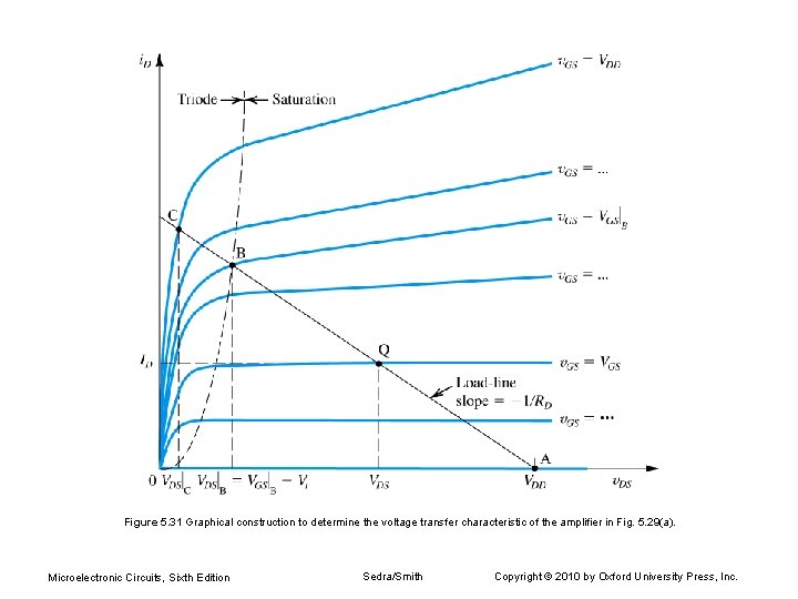
Figure 5. 31 Graphical construction to determine the voltage transfer characteristic of the amplifier in Fig. 5. 29(a). Microelectronic Circuits, Sixth Edition Sedra/Smith Copyright © 2010 by Oxford University Press, Inc.

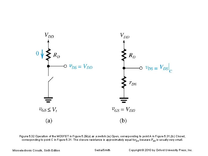
Figure 5. 32 Operation of the MOSFET in Figure 5. 29(a) as a switch: (a) Open, corresponding to point A in Figure 5. 31; (b) Closed, corresponding to point C in Figure 5. 31. The closure resistance is approximately equal to r. DS because VDS is usually very small. Microelectronic Circuits, Sixth Edition Sedra/Smith Copyright © 2010 by Oxford University Press, Inc.

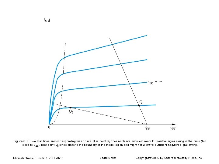
Figure 5. 33 Two load lines and corresponding bias points. Bias point Q 1 does not leave sufficient room for positive signal swing at the drain (too close to VDD). Bias point Q 2 is too close to the boundary of the triode region and might not allow for sufficient negative signal swing. Microelectronic Circuits, Sixth Edition Sedra/Smith Copyright © 2010 by Oxford University Press, Inc.

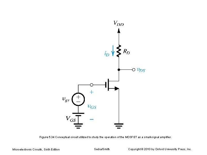
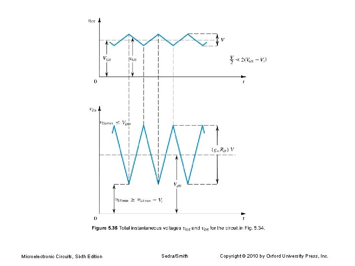
Figure 5. 34 Conceptual circuit utilized to study the operation of the MOSFET as a small-signal amplifier. Microelectronic Circuits, Sixth Edition Sedra/Smith Copyright © 2010 by Oxford University Press, Inc.

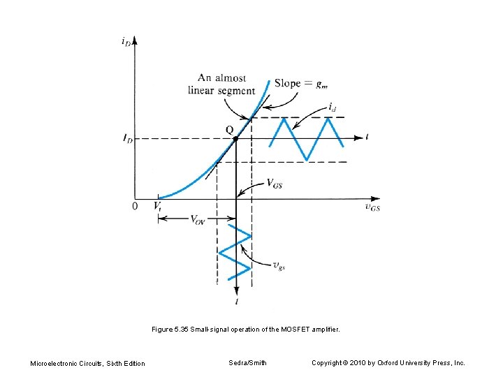
Figure 5. 35 Small-signal operation of the MOSFET amplifier. Microelectronic Circuits, Sixth Edition Sedra/Smith Copyright © 2010 by Oxford University Press, Inc.

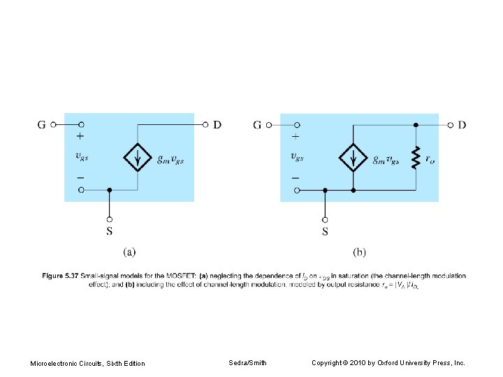
Microelectronic Circuits, Sixth Edition Sedra/Smith Copyright © 2010 by Oxford University Press, Inc.

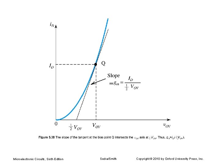
Microelectronic Circuits, Sixth Edition Sedra/Smith Copyright © 2010 by Oxford University Press, Inc.

Microelectronic Circuits, Sixth Edition Sedra/Smith Copyright © 2010 by Oxford University Press, Inc.

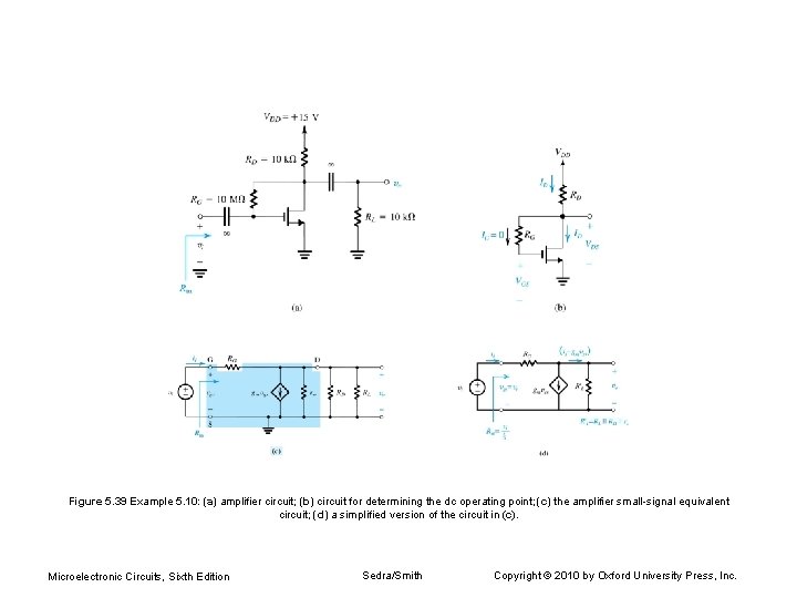
Figure 5. 39 Example 5. 10: (a) amplifier circuit; (b) circuit for determining the dc operating point; (c) the amplifier small-signal equivalent circuit; (d) a simplified version of the circuit in (c). Microelectronic Circuits, Sixth Edition Sedra/Smith Copyright © 2010 by Oxford University Press, Inc.

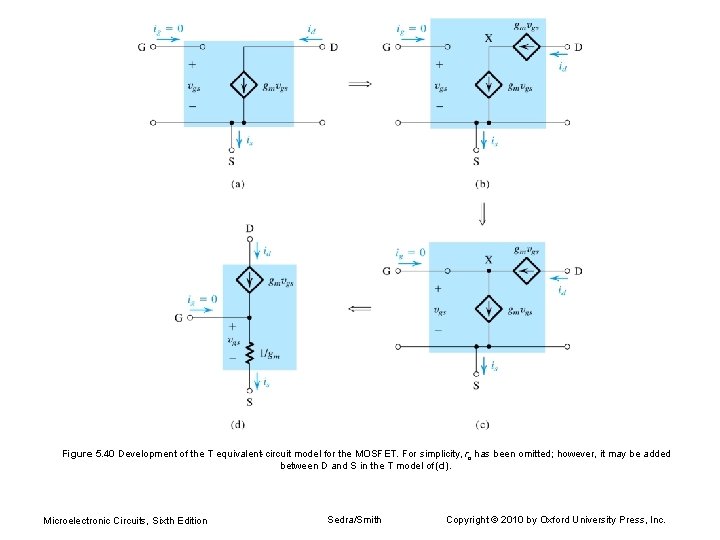
Figure 5. 40 Development of the T equivalent-circuit model for the MOSFET. For simplicity, ro has been omitted; however, it may be added between D and S in the T model of (d). Microelectronic Circuits, Sixth Edition Sedra/Smith Copyright © 2010 by Oxford University Press, Inc.

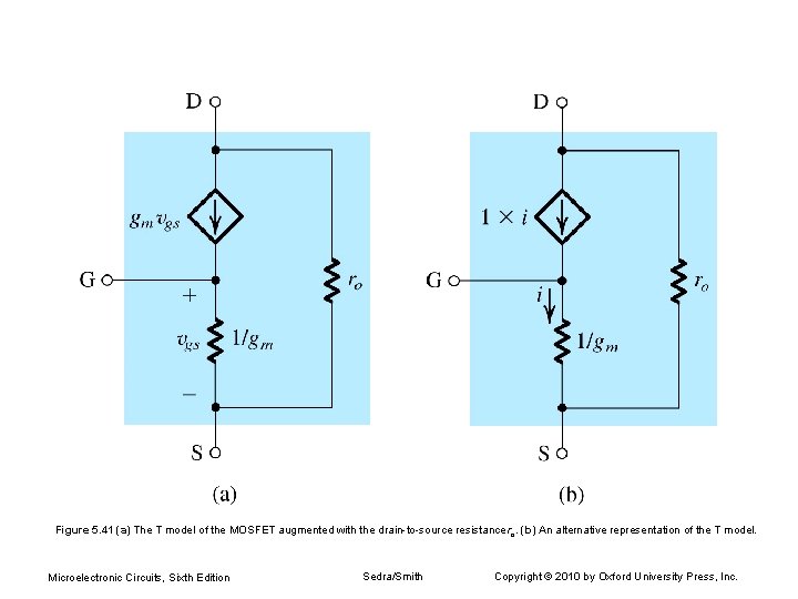
Figure 5. 41 (a) The T model of the MOSFET augmented with the drain-to-source resistance ro. (b) An alternative representation of the T model. Microelectronic Circuits, Sixth Edition Sedra/Smith Copyright © 2010 by Oxford University Press, Inc.

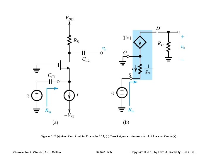
Figure 5. 42 (a) Amplifier circuit for Example 5. 11; (b) Small-signal equivalent circuit of the amplifier in (a). Microelectronic Circuits, Sixth Edition Sedra/Smith Copyright © 2010 by Oxford University Press, Inc.

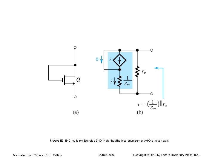
Figure E 5. 19 Circuits for Exercise 5. 19. Note that the bias arrangement of Q is not shown. Microelectronic Circuits, Sixth Edition Sedra/Smith Copyright © 2010 by Oxford University Press, Inc.

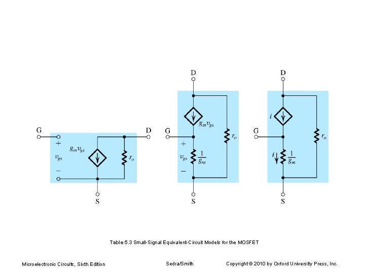
Table 5. 3 Small-Signal Equivalent-Circuit Models for the MOSFET Microelectronic Circuits, Sixth Edition Sedra/Smith Copyright © 2010 by Oxford University Press, Inc.

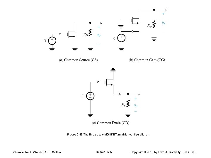
Figure 5. 43 The three basic MOSFET amplifier configurations. Microelectronic Circuits, Sixth Edition Sedra/Smith Copyright © 2010 by Oxford University Press, Inc.

Microelectronic Circuits, Sixth Edition Sedra/Smith Copyright © 2010 by Oxford University Press, Inc.

Microelectronic Circuits, Sixth Edition Sedra/Smith Copyright © 2010 by Oxford University Press, Inc.

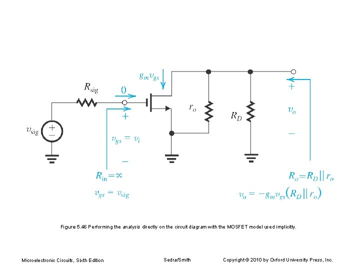
Figure 5. 46 Performing the analysis directly on the circuit diagram with the MOSFET model used implicitly. Microelectronic Circuits, Sixth Edition Sedra/Smith Copyright © 2010 by Oxford University Press, Inc.

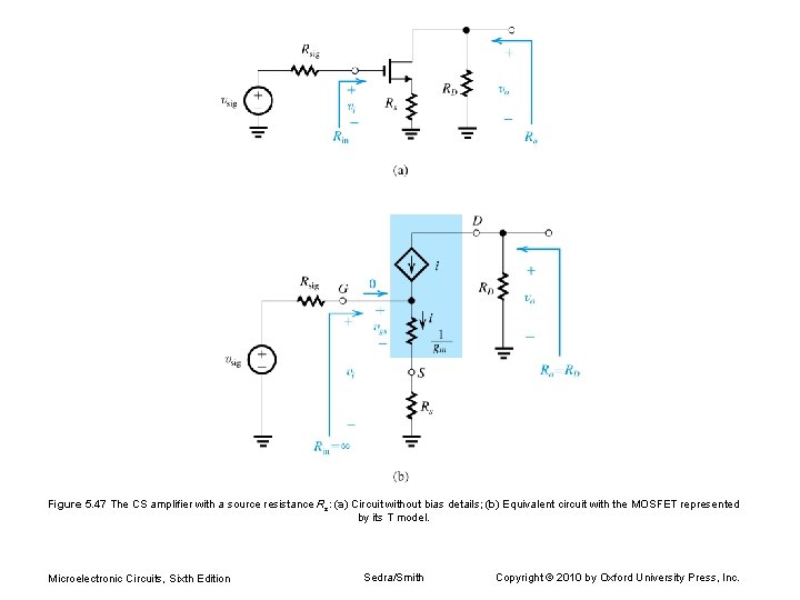
Figure 5. 47 The CS amplifier with a source resistance Rs: (a) Circuit without bias details; (b) Equivalent circuit with the MOSFET represented by its T model. Microelectronic Circuits, Sixth Edition Sedra/Smith Copyright © 2010 by Oxford University Press, Inc.

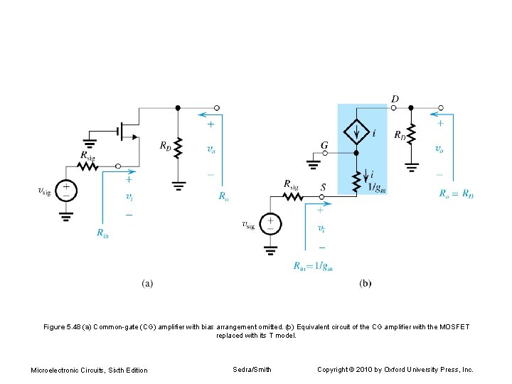
Figure 5. 48 (a) Common-gate (CG) amplifier with bias arrangement omitted. (b) Equivalent circuit of the CG amplifier with the MOSFET replaced with its T model. Microelectronic Circuits, Sixth Edition Sedra/Smith Copyright © 2010 by Oxford University Press, Inc.

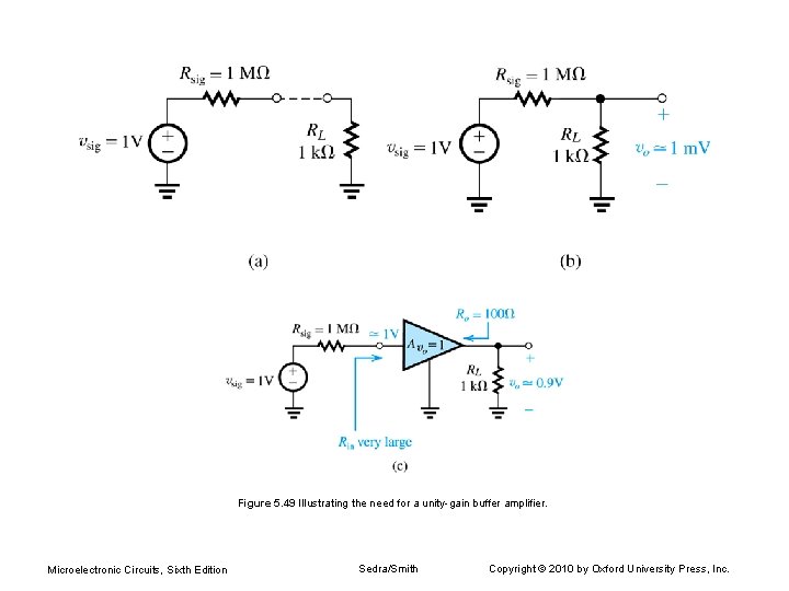
Figure 5. 49 Illustrating the need for a unity-gain buffer amplifier. Microelectronic Circuits, Sixth Edition Sedra/Smith Copyright © 2010 by Oxford University Press, Inc.

Microelectronic Circuits, Sixth Edition Sedra/Smith Copyright © 2010 by Oxford University Press, Inc.

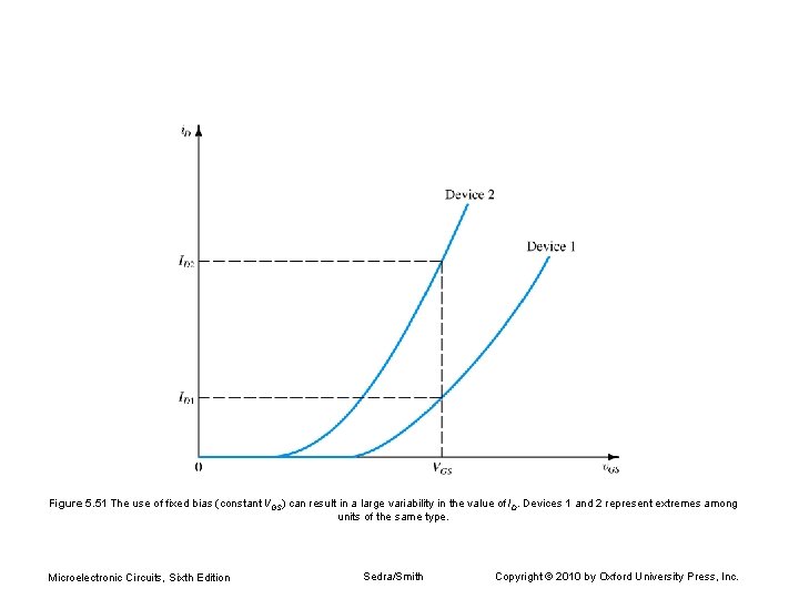
Figure 5. 51 The use of fixed bias (constant VGS) can result in a large variability in the value of ID. Devices 1 and 2 represent extremes among units of the same type. Microelectronic Circuits, Sixth Edition Sedra/Smith Copyright © 2010 by Oxford University Press, Inc.

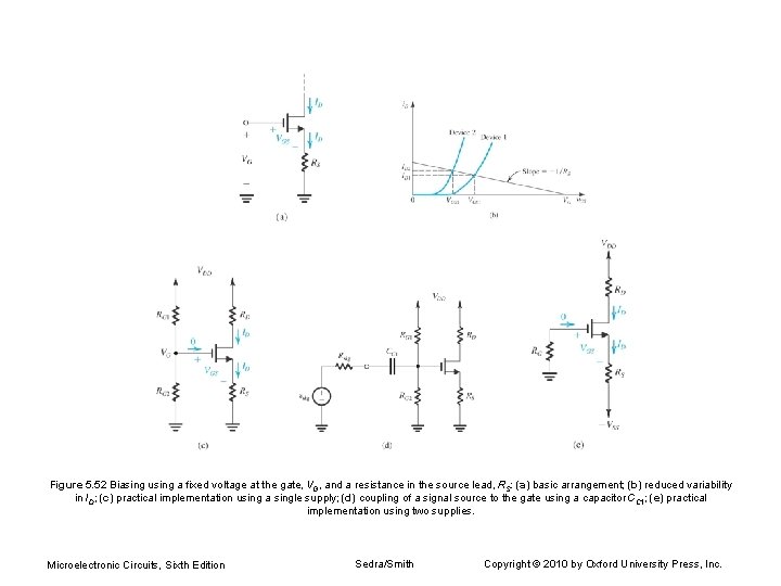
Figure 5. 52 Biasing using a fixed voltage at the gate, VG, and a resistance in the source lead, RS: (a) basic arrangement; (b) reduced variability in ID; (c) practical implementation using a single supply; (d) coupling of a signal source to the gate using a capacitor CC 1; (e) practical implementation using two supplies. Microelectronic Circuits, Sixth Edition Sedra/Smith Copyright © 2010 by Oxford University Press, Inc.

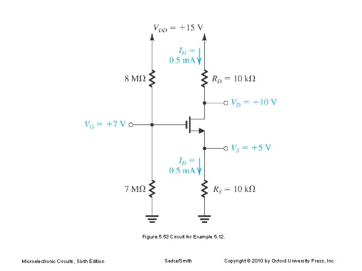
Figure 5. 53 Circuit for Example 5. 12. Microelectronic Circuits, Sixth Edition Sedra/Smith Copyright © 2010 by Oxford University Press, Inc.

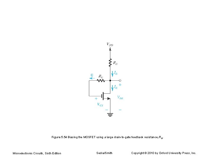
Figure 5. 54 Biasing the MOSFET using a large drain-to-gate feedback resistance, RG. Microelectronic Circuits, Sixth Edition Sedra/Smith Copyright © 2010 by Oxford University Press, Inc.

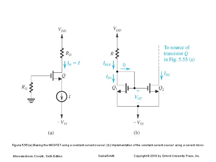
Figure 5. 55 (a) Biasing the MOSFET using a constant-current source I. (b) Implementation of the constant-current source I using a current mirror. Microelectronic Circuits, Sixth Edition Sedra/Smith Copyright © 2010 by Oxford University Press, Inc.

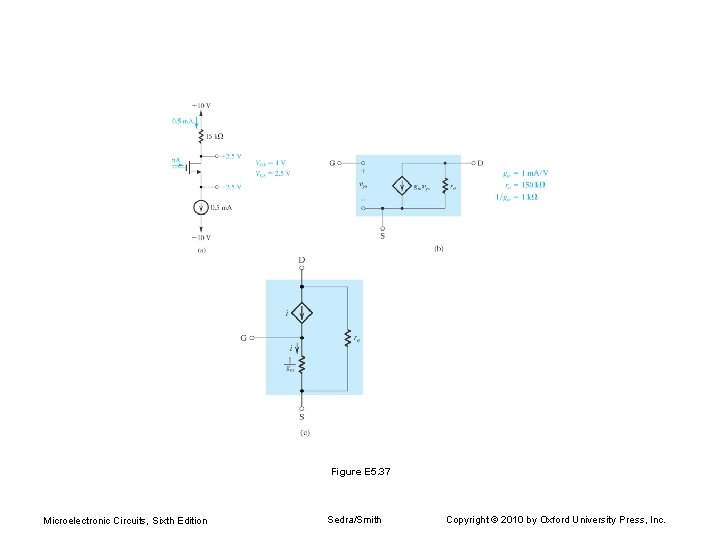
Figure E 5. 37 Microelectronic Circuits, Sixth Edition Sedra/Smith Copyright © 2010 by Oxford University Press, Inc.

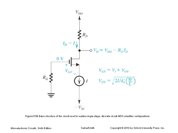
Figure 5. 56 Basic structure of the circuit used to realize single-stage, discrete-circuit MOS amplifier configurations. Microelectronic Circuits, Sixth Edition Sedra/Smith Copyright © 2010 by Oxford University Press, Inc.

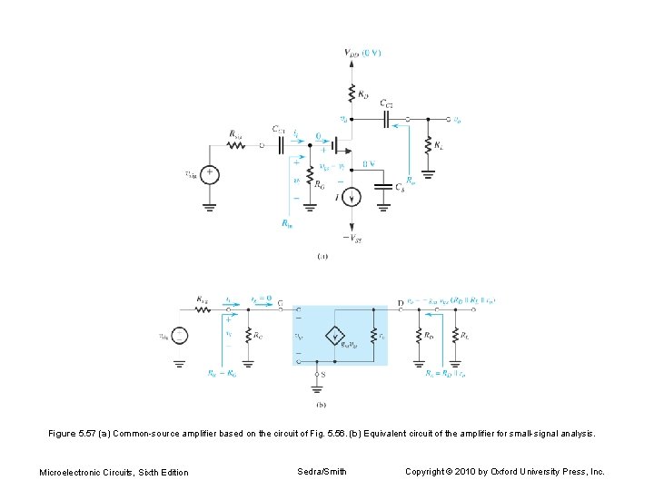
Figure 5. 57 (a) Common-source amplifier based on the circuit of Fig. 5. 56. (b) Equivalent circuit of the amplifier for small-signal analysis. Microelectronic Circuits, Sixth Edition Sedra/Smith Copyright © 2010 by Oxford University Press, Inc.

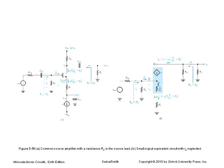
Figure 5. 58 (a) Common-source amplifier with a resistance RS in the source lead. (b) Small-signal equivalent circuit with ro neglected. Microelectronic Circuits, Sixth Edition Sedra/Smith Copyright © 2010 by Oxford University Press, Inc.

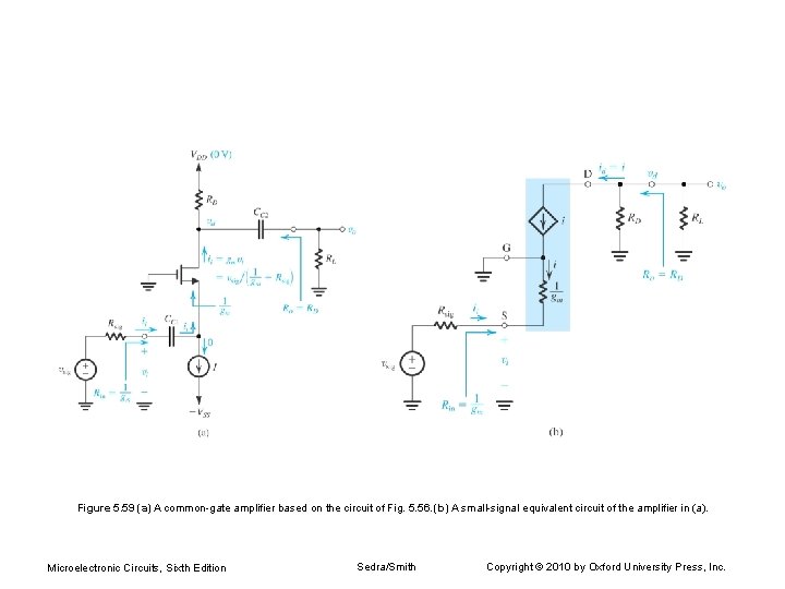
Figure 5. 59 (a) A common-gate amplifier based on the circuit of Fig. 5. 56. (b) A small-signal equivalent circuit of the amplifier in (a). Microelectronic Circuits, Sixth Edition Sedra/Smith Copyright © 2010 by Oxford University Press, Inc.

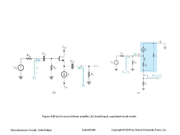
Figure 5. 60 (a) A source-follower amplifier. (b) Small-signal, equivalent-circuit model. Microelectronic Circuits, Sixth Edition Sedra/Smith Copyright © 2010 by Oxford University Press, Inc.

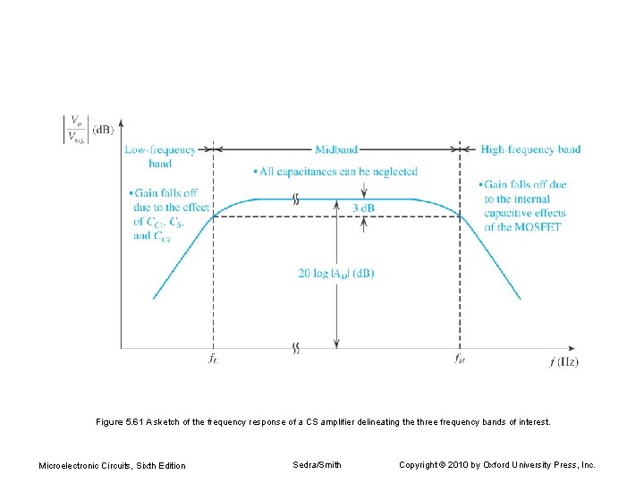
Figure 5. 61 A sketch of the frequency response of a CS amplifier delineating the three frequency bands of interest. Microelectronic Circuits, Sixth Edition Sedra/Smith Copyright © 2010 by Oxford University Press, Inc.

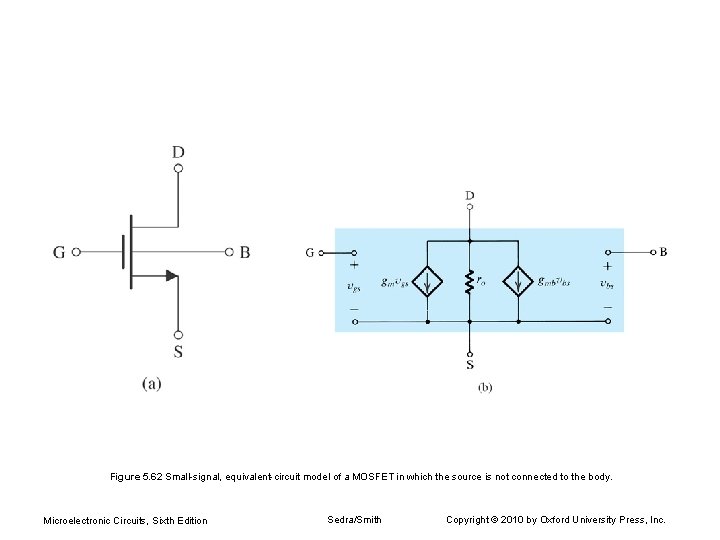
Figure 5. 62 Small-signal, equivalent-circuit model of a MOSFET in which the source is not connected to the body. Microelectronic Circuits, Sixth Edition Sedra/Smith Copyright © 2010 by Oxford University Press, Inc.

Microelectronic Circuits, Sixth Edition Sedra/Smith Copyright © 2010 by Oxford University Press, Inc.

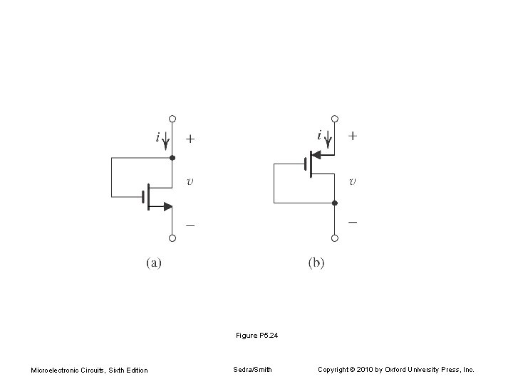
Figure P 5. 24 Microelectronic Circuits, Sixth Edition Sedra/Smith Copyright © 2010 by Oxford University Press, Inc.

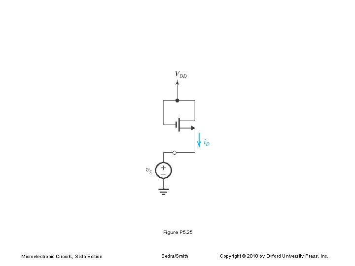
Figure P 5. 25 Microelectronic Circuits, Sixth Edition Sedra/Smith Copyright © 2010 by Oxford University Press, Inc.

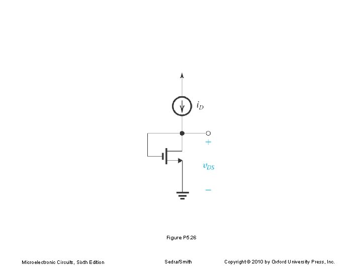
Figure P 5. 26 Microelectronic Circuits, Sixth Edition Sedra/Smith Copyright © 2010 by Oxford University Press, Inc.

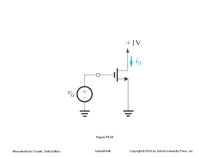
Figure P 5. 28 Microelectronic Circuits, Sixth Edition Sedra/Smith Copyright © 2010 by Oxford University Press, Inc.

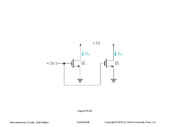
Figure P 5. 29 Microelectronic Circuits, Sixth Edition Sedra/Smith Copyright © 2010 by Oxford University Press, Inc.

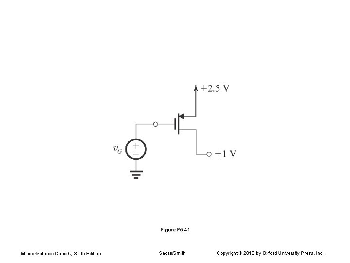
Figure P 5. 41 Microelectronic Circuits, Sixth Edition Sedra/Smith Copyright © 2010 by Oxford University Press, Inc.

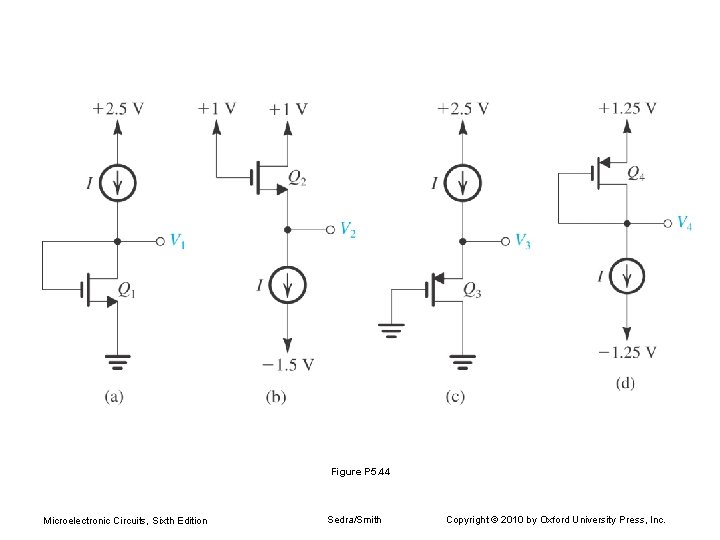
Figure P 5. 44 Microelectronic Circuits, Sixth Edition Sedra/Smith Copyright © 2010 by Oxford University Press, Inc.

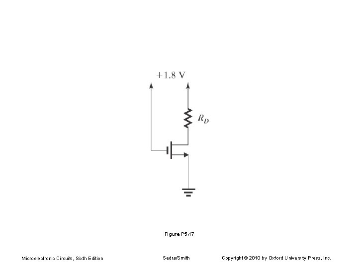
Figure P 5. 47 Microelectronic Circuits, Sixth Edition Sedra/Smith Copyright © 2010 by Oxford University Press, Inc.

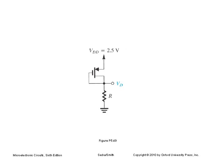
Figure P 5. 49 Microelectronic Circuits, Sixth Edition Sedra/Smith Copyright © 2010 by Oxford University Press, Inc.

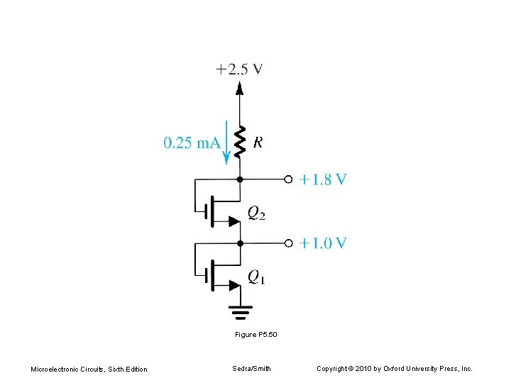
Figure P 5. 50 Microelectronic Circuits, Sixth Edition Sedra/Smith Copyright © 2010 by Oxford University Press, Inc.

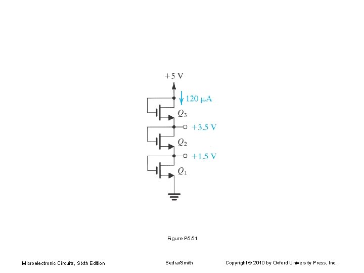
Figure P 5. 51 Microelectronic Circuits, Sixth Edition Sedra/Smith Copyright © 2010 by Oxford University Press, Inc.

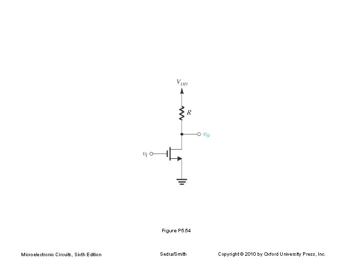
Figure P 5. 54 Microelectronic Circuits, Sixth Edition Sedra/Smith Copyright © 2010 by Oxford University Press, Inc.

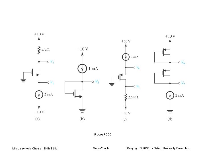
Figure P 5. 55 Microelectronic Circuits, Sixth Edition Sedra/Smith Copyright © 2010 by Oxford University Press, Inc.

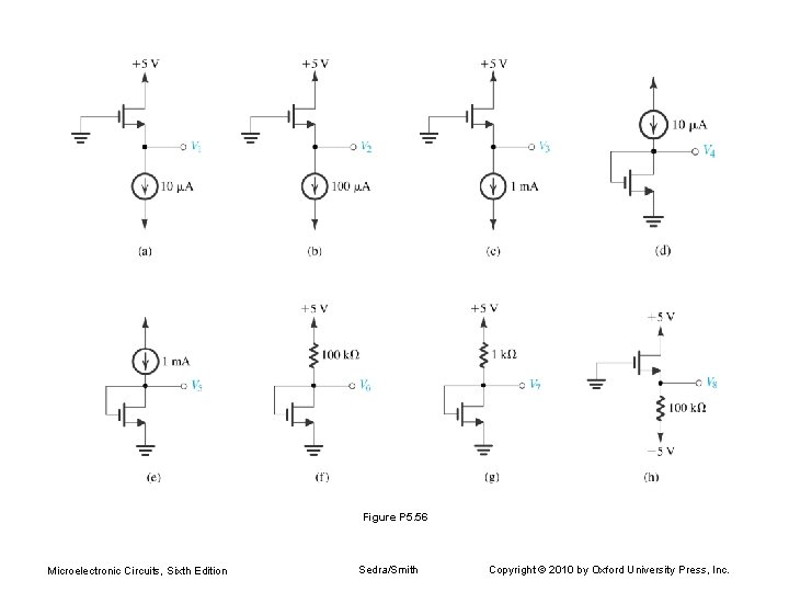
Figure P 5. 56 Microelectronic Circuits, Sixth Edition Sedra/Smith Copyright © 2010 by Oxford University Press, Inc.

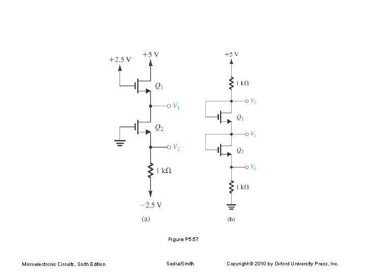
Figure P 5. 57 Microelectronic Circuits, Sixth Edition Sedra/Smith Copyright © 2010 by Oxford University Press, Inc.

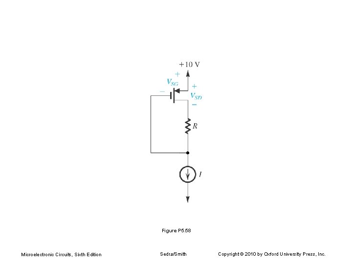
Figure P 5. 58 Microelectronic Circuits, Sixth Edition Sedra/Smith Copyright © 2010 by Oxford University Press, Inc.

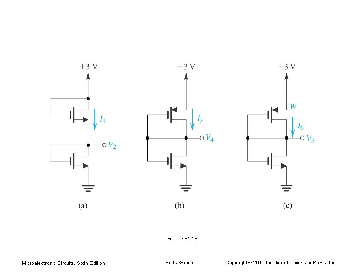
Figure P 5. 59 Microelectronic Circuits, Sixth Edition Sedra/Smith Copyright © 2010 by Oxford University Press, Inc.

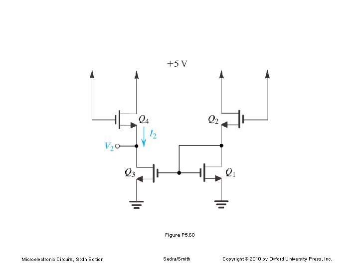
Figure P 5. 60 Microelectronic Circuits, Sixth Edition Sedra/Smith Copyright © 2010 by Oxford University Press, Inc.

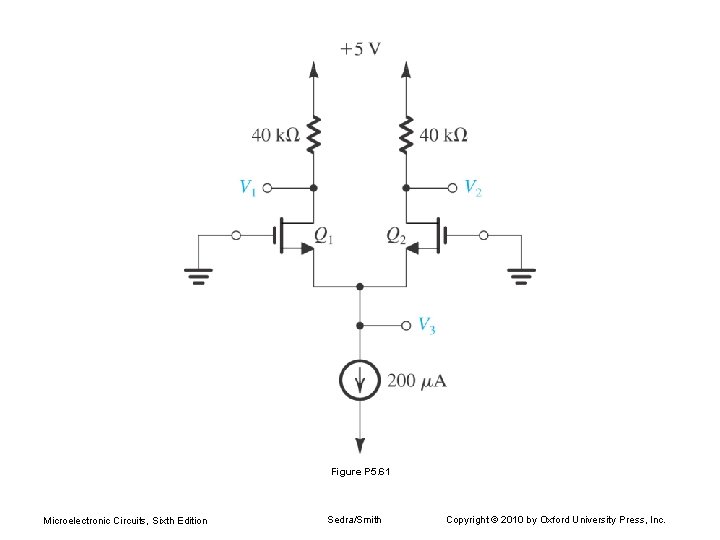
Figure P 5. 61 Microelectronic Circuits, Sixth Edition Sedra/Smith Copyright © 2010 by Oxford University Press, Inc.

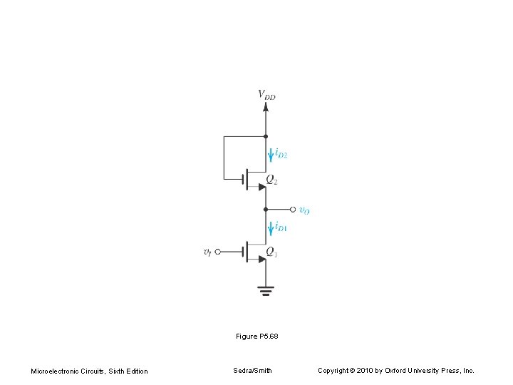
Figure P 5. 68 Microelectronic Circuits, Sixth Edition Sedra/Smith Copyright © 2010 by Oxford University Press, Inc.

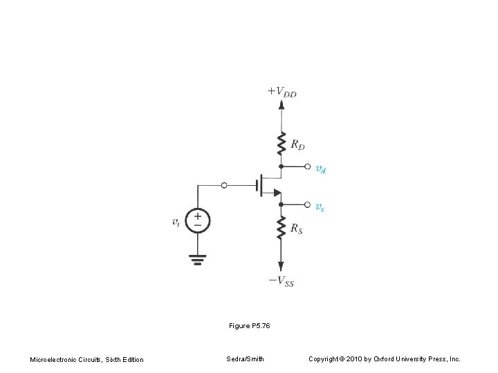
Figure P 5. 76 Microelectronic Circuits, Sixth Edition Sedra/Smith Copyright © 2010 by Oxford University Press, Inc.

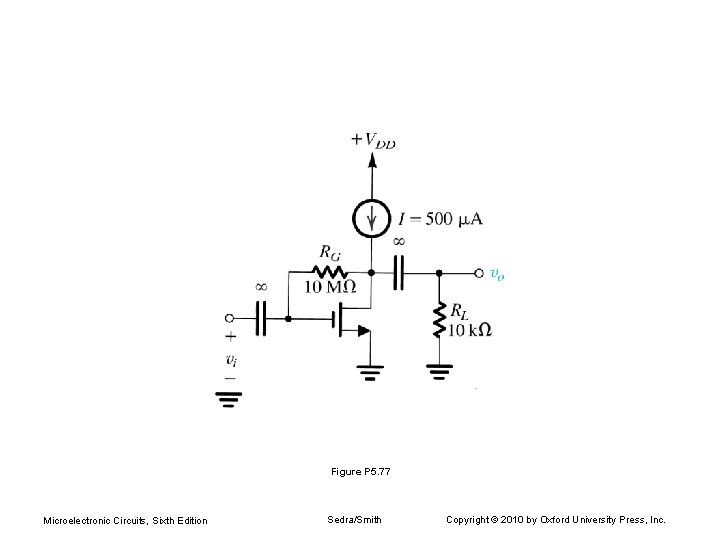
Figure P 5. 77 Microelectronic Circuits, Sixth Edition Sedra/Smith Copyright © 2010 by Oxford University Press, Inc.

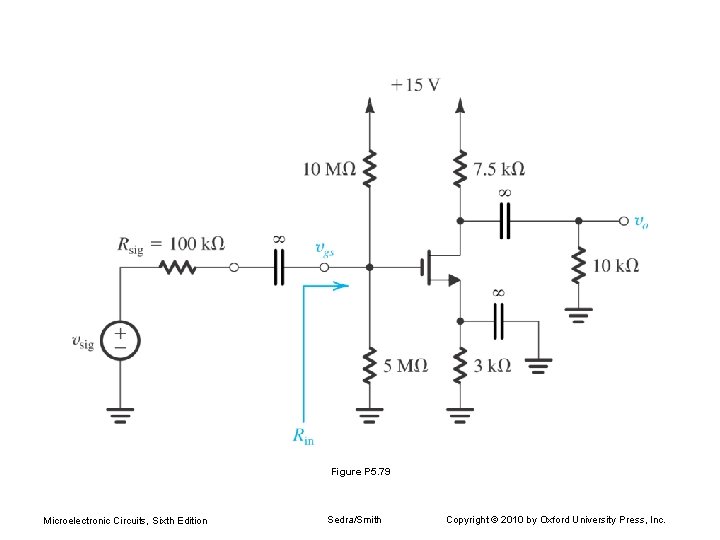
Figure P 5. 79 Microelectronic Circuits, Sixth Edition Sedra/Smith Copyright © 2010 by Oxford University Press, Inc.

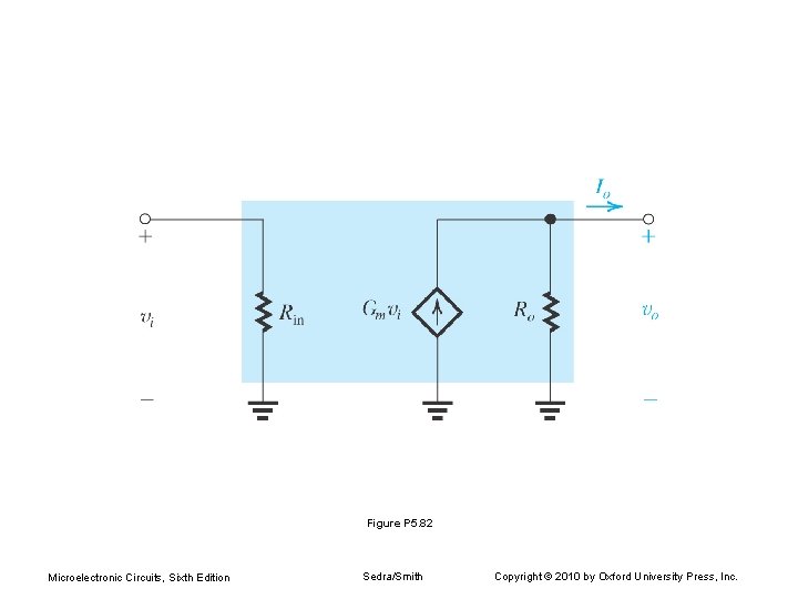
Figure P 5. 82 Microelectronic Circuits, Sixth Edition Sedra/Smith Copyright © 2010 by Oxford University Press, Inc.

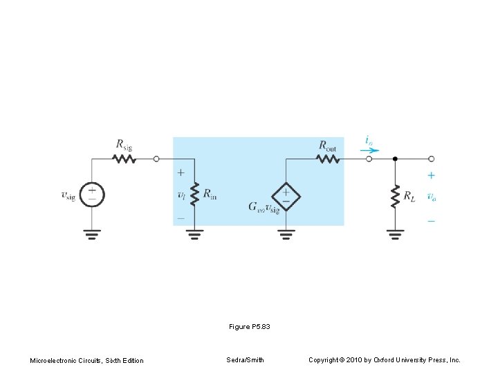
Figure P 5. 83 Microelectronic Circuits, Sixth Edition Sedra/Smith Copyright © 2010 by Oxford University Press, Inc.

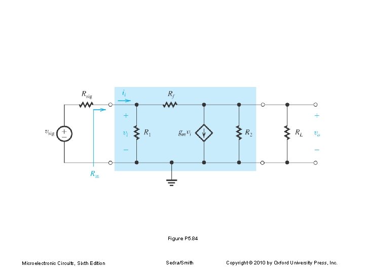
Figure P 5. 84 Microelectronic Circuits, Sixth Edition Sedra/Smith Copyright © 2010 by Oxford University Press, Inc.

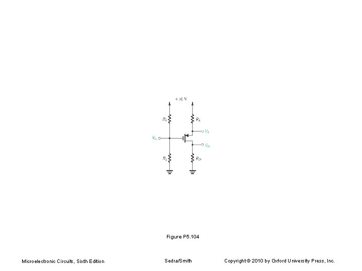
Figure P 5. 104 Microelectronic Circuits, Sixth Edition Sedra/Smith Copyright © 2010 by Oxford University Press, Inc.

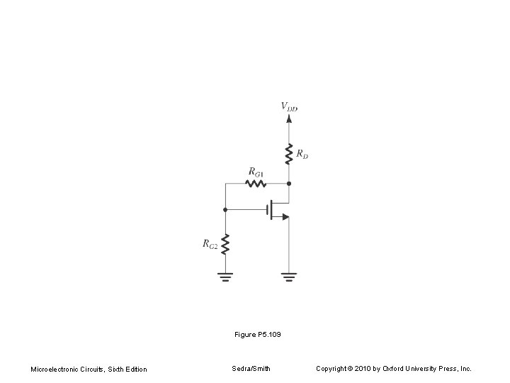
Figure P 5. 109 Microelectronic Circuits, Sixth Edition Sedra/Smith Copyright © 2010 by Oxford University Press, Inc.

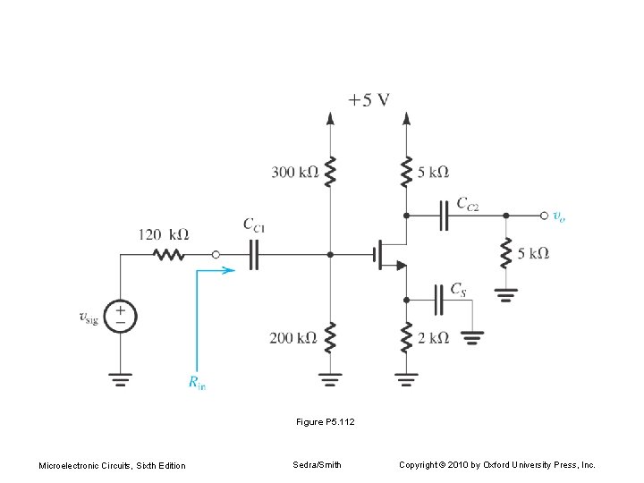
Figure P 5. 112 Microelectronic Circuits, Sixth Edition Sedra/Smith Copyright © 2010 by Oxford University Press, Inc.

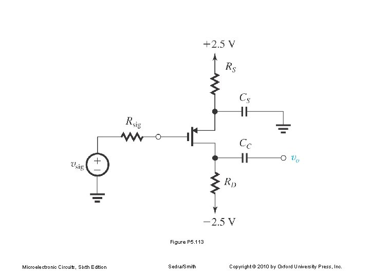
Figure P 5. 113 Microelectronic Circuits, Sixth Edition Sedra/Smith Copyright © 2010 by Oxford University Press, Inc.

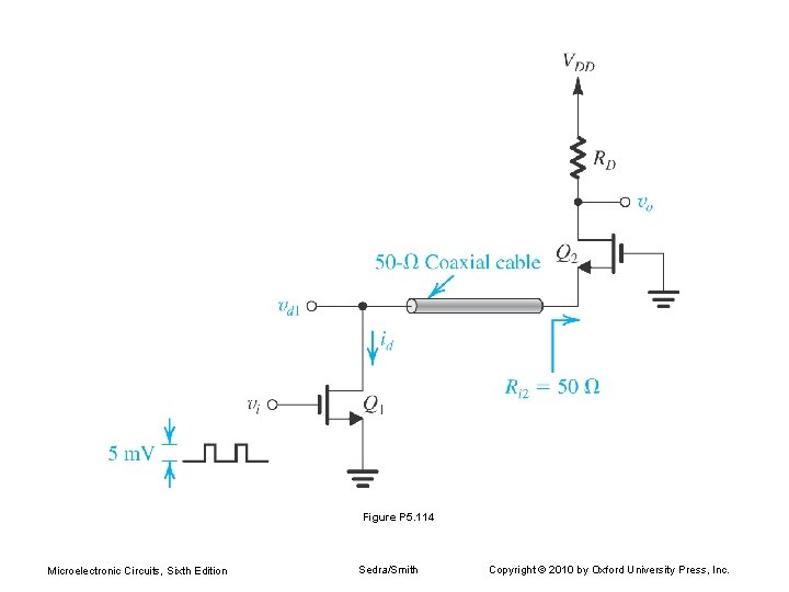
Figure P 5. 114 Microelectronic Circuits, Sixth Edition Sedra/Smith Copyright © 2010 by Oxford University Press, Inc.

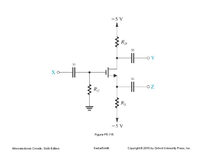
Figure P 5. 115 Microelectronic Circuits, Sixth Edition Sedra/Smith Copyright © 2010 by Oxford University Press, Inc.

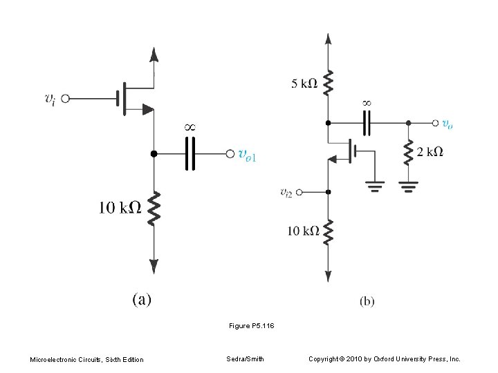
Figure P 5. 116 Microelectronic Circuits, Sixth Edition Sedra/Smith Copyright © 2010 by Oxford University Press, Inc.

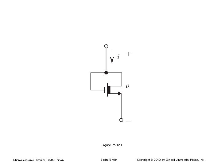
Figure P 5. 123 Microelectronic Circuits, Sixth Edition Sedra/Smith Copyright © 2010 by Oxford University Press, Inc.

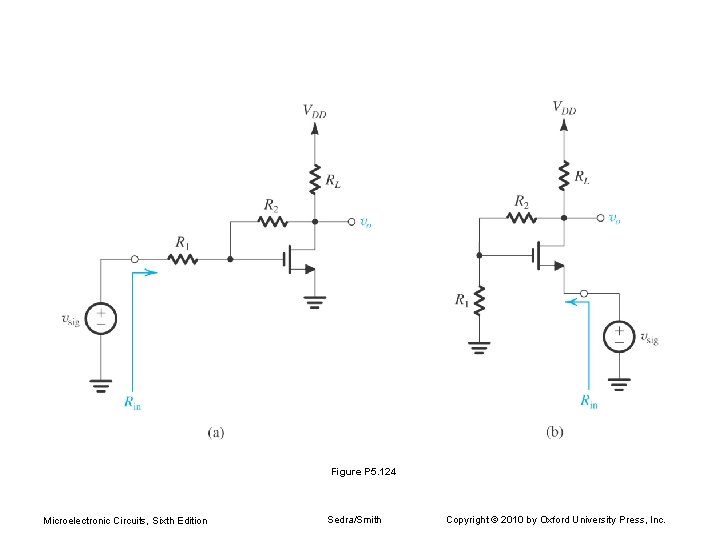
Figure P 5. 124 Microelectronic Circuits, Sixth Edition Sedra/Smith Copyright © 2010 by Oxford University Press, Inc.

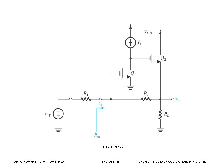
Figure P 5. 126 Microelectronic Circuits, Sixth Edition Sedra/Smith Copyright © 2010 by Oxford University Press, Inc.