Lecture 32 OUTLINE The MOS Capacitor Capacitancevoltage CV
- Slides: 14

Lecture #32 OUTLINE The MOS Capacitor: • Capacitance-voltage (C-V) characteristics Reading: Chapter 16. 4 1 Spring 2007 EE 130 Lecture 32, Slide 1

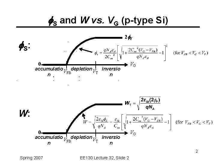
f. S and W vs. VG (p-type Si) 2 f. F f S: 0 VG accumulatio V depletion V inversio FB T n n W: accumulatio VFBdepletion VT inversio n n 2 Spring 2007 EE 130 Lecture 32, Slide 2

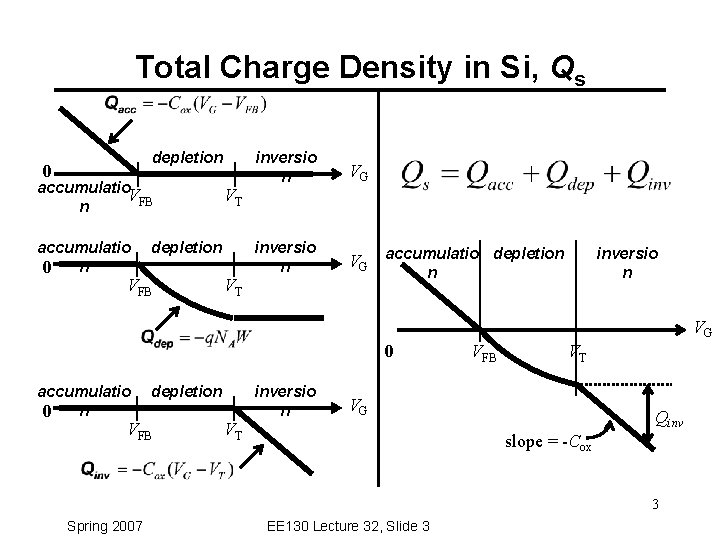
Total Charge Density in Si, Qs depletion 0 accumulatio VFB n accumulatio 0 n VT depletion VFB VT inversio n VG accumulatio depletion inversio n n VG 0 accumulatio 0 n depletion VFB VT inversio n VFB VT VG Qinv slope = -Cox 3 Spring 2007 EE 130 Lecture 32, Slide 3

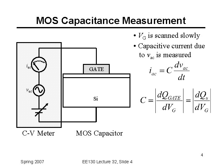
MOS Capacitance Measurement • VG is scanned slowly • Capacitive current due to vac is measured iac GATE vac Si C-V Meter MOS Capacitor 4 Spring 2007 EE 130 Lecture 32, Slide 4

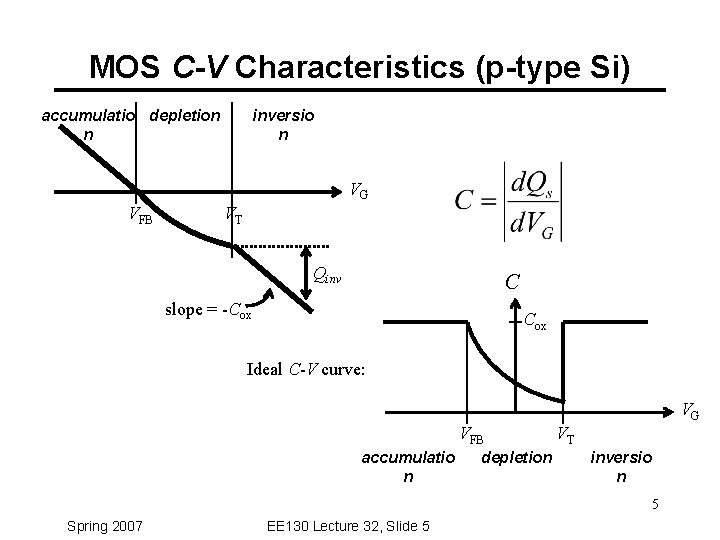
MOS C-V Characteristics (p-type Si) accumulatio depletion n inversio n VG VFB VT Qinv C slope = -Cox Ideal C-V curve: VG VFB accumulatio n depletion VT inversio n 5 Spring 2007 EE 130 Lecture 32, Slide 5

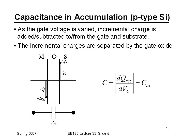
Capacitance in Accumulation (p-type Si) • As the gate voltage is varied, incremental charge is added/subtracted to/from the gate and substrate. • The incremental charges are separated by the gate oxide. M O S DQ Q -Q -DQ Cox 6 Spring 2007 EE 130 Lecture 32, Slide 6

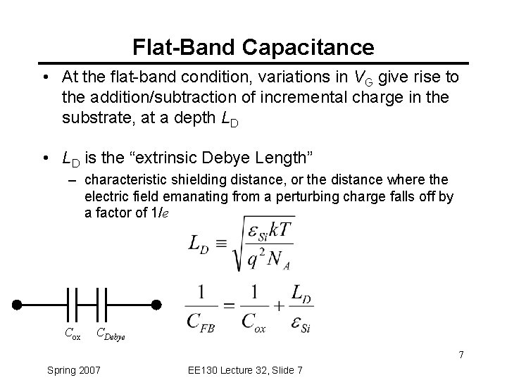
Flat-Band Capacitance • At the flat-band condition, variations in VG give rise to the addition/subtraction of incremental charge in the substrate, at a depth LD • LD is the “extrinsic Debye Length” – characteristic shielding distance, or the distance where the electric field emanating from a perturbing charge falls off by a factor of 1/e Cox CDebye 7 Spring 2007 EE 130 Lecture 32, Slide 7

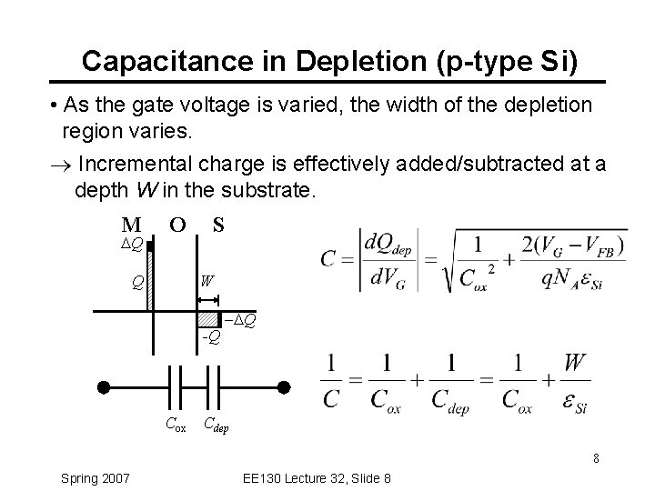
Capacitance in Depletion (p-type Si) • As the gate voltage is varied, the width of the depletion region varies. ® Incremental charge is effectively added/subtracted at a depth W in the substrate. M DQ Q O S W -Q -DQ Cox Cdep 8 Spring 2007 EE 130 Lecture 32, Slide 8

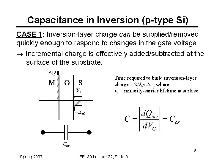
Capacitance in Inversion (p-type Si) CASE 1: Inversion-layer charge can be supplied/removed quickly enough to respond to changes in the gate voltage. ® Incremental charge is effectively added/subtracted at the surface of the substrate. DQ M O S WT Time required to build inversion-layer charge = 2 NAto/ni , where to = minority-carrier lifetime at surface -DQ Cox 9 Spring 2007 EE 130 Lecture 32, Slide 9

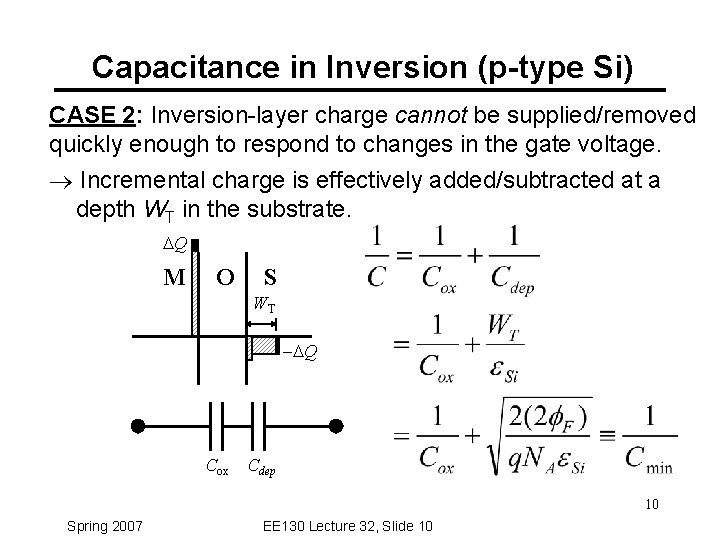
Capacitance in Inversion (p-type Si) CASE 2: Inversion-layer charge cannot be supplied/removed quickly enough to respond to changes in the gate voltage. ® Incremental charge is effectively added/subtracted at a depth WT in the substrate. DQ M O S WT -DQ Cox Cdep 10 Spring 2007 EE 130 Lecture 32, Slide 10

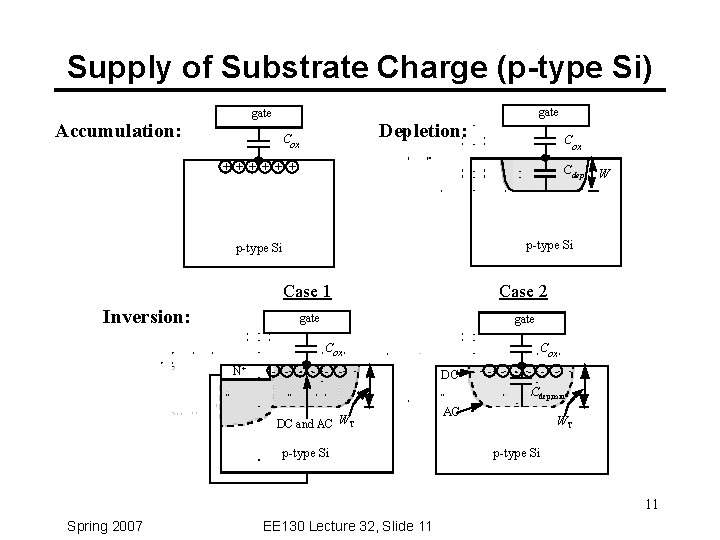
Supply of Substrate Charge (p-type Si) gate Accumulation: Depletion: Cox + + + C dep p-type Si Inversion: Case 1 Case 2 gate Cox N+ W - - - DC and AC WT p-type Si Cox DC AC - - - Cdep, min WT p-type Si 11 Spring 2007 EE 130 Lecture 32, Slide 11

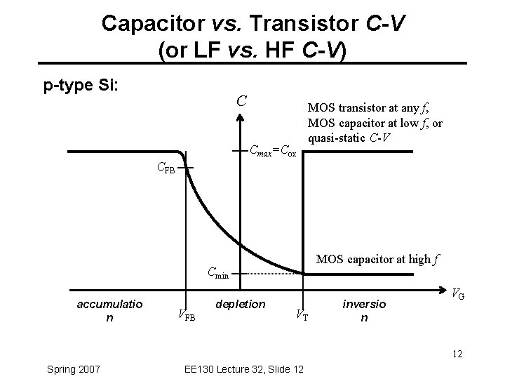
Capacitor vs. Transistor C-V (or LF vs. HF C-V) p-type Si: C Cmax=Cox MOS transistor at any f, MOS capacitor at low f, or quasi-static C-V CFB MOS capacitor at high f Cmin accumulatio n VFB depletion VT inversio n VG 12 Spring 2007 EE 130 Lecture 32, Slide 12

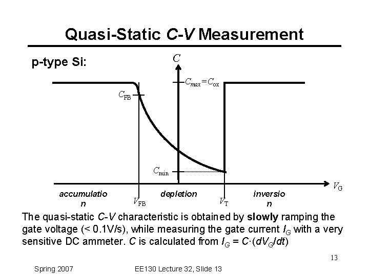
Quasi-Static C-V Measurement C p-type Si: Cmax=Cox CFB Cmin accumulatio n VFB depletion VT inversio n VG The quasi-static C-V characteristic is obtained by slowly ramping the gate voltage (< 0. 1 V/s), while measuring the gate current IG with a very sensitive DC ammeter. C is calculated from IG = C·(d. VG/dt) 13 Spring 2007 EE 130 Lecture 32, Slide 13

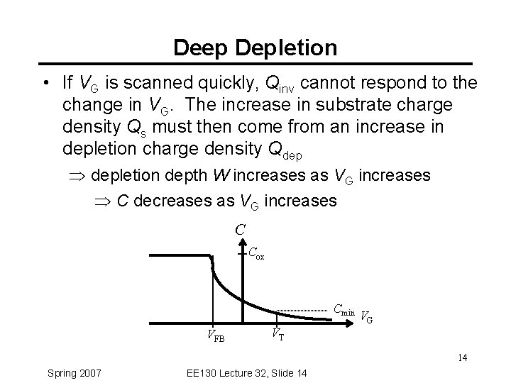
Deep Depletion • If VG is scanned quickly, Qinv cannot respond to the change in VG. The increase in substrate charge density Qs must then come from an increase in depletion charge density Qdep Þ depletion depth W increases as VG increases Þ C decreases as VG increases C Cox Cmin VFB VG VT 14 Spring 2007 EE 130 Lecture 32, Slide 14