Diodes Microelectronic Circuits Fifth Edition SedraSmith 1 Figure

- Slides: 97

Diodes Microelectronic Circuits - Fifth Edition Sedra/Smith 1

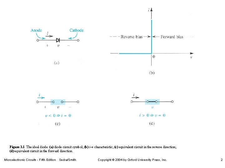
Figure 3. 1 The ideal diode: (a) diode circuit symbol; (b) i–v characteristic; (c) equivalent circuit in the reverse direction; (d) equivalent circuit in the forward direction. Microelectronic Circuits - Fifth Edition Sedra/Smith Copyright 2004 by Oxford University Press, Inc. 2

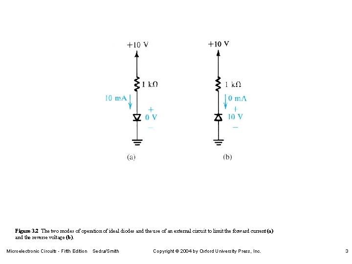
Figure 3. 2 The two modes of operation of ideal diodes and the use of an external circuit to limit the forward current (a) and the reverse voltage (b). Microelectronic Circuits - Fifth Edition Sedra/Smith Copyright 2004 by Oxford University Press, Inc. 3

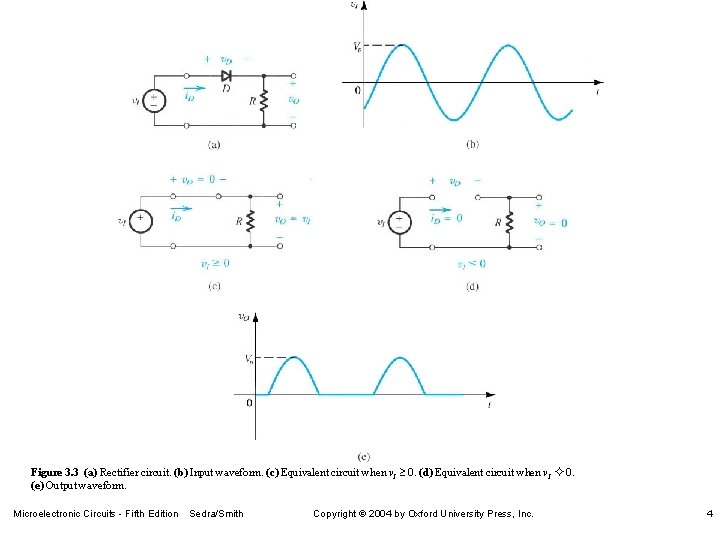
Figure 3. 3 (a) Rectifier circuit. (b) Input waveform. (c) Equivalent circuit when v. I 0. (d) Equivalent circuit when v. I 0. (e) Output waveform. Microelectronic Circuits - Fifth Edition Sedra/Smith Copyright 2004 by Oxford University Press, Inc. 4

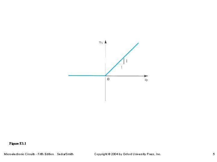
Figure E 3. 1 Microelectronic Circuits - Fifth Edition Sedra/Smith Copyright 2004 by Oxford University Press, Inc. 5

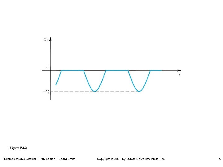
Figure E 3. 2 Microelectronic Circuits - Fifth Edition Sedra/Smith Copyright 2004 by Oxford University Press, Inc. 6

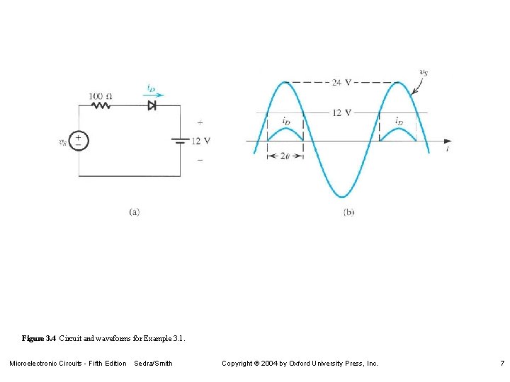
Figure 3. 4 Circuit and waveforms for Example 3. 1. Microelectronic Circuits - Fifth Edition Sedra/Smith Copyright 2004 by Oxford University Press, Inc. 7

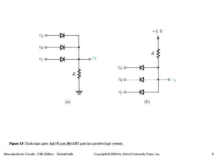
Figure 3. 5 Diode logic gates: (a) OR gate; (b) AND gate (in a positive-logic system). Microelectronic Circuits - Fifth Edition Sedra/Smith Copyright 2004 by Oxford University Press, Inc. 8

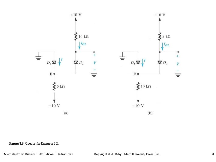
Figure 3. 6 Circuits for Example 3. 2. Microelectronic Circuits - Fifth Edition Sedra/Smith Copyright 2004 by Oxford University Press, Inc. 9

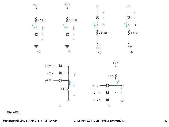
Figure E 3. 4 Microelectronic Circuits - Fifth Edition Sedra/Smith Copyright 2004 by Oxford University Press, Inc. 10

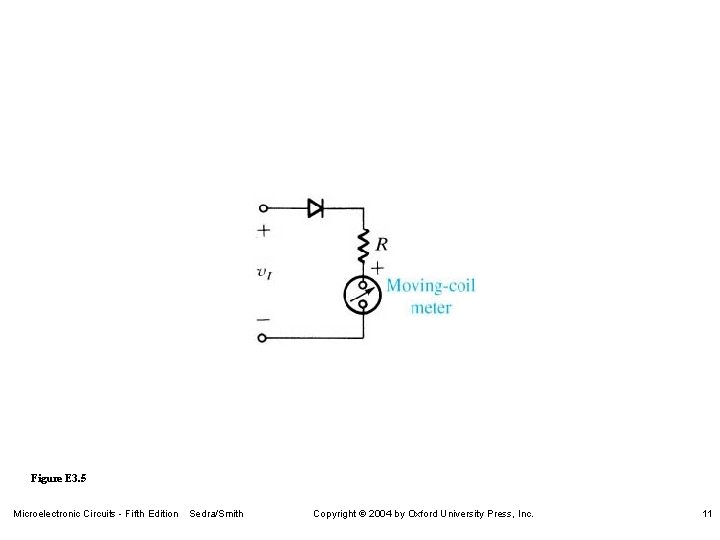
Figure E 3. 5 Microelectronic Circuits - Fifth Edition Sedra/Smith Copyright 2004 by Oxford University Press, Inc. 11

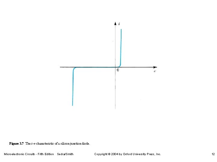
Figure 3. 7 The i–v characteristic of a silicon junction diode. Microelectronic Circuits - Fifth Edition Sedra/Smith Copyright 2004 by Oxford University Press, Inc. 12

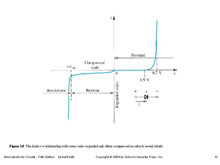
Figure 3. 8 The diode i–v relationship with some scales expanded and others compressed in order to reveal details. Microelectronic Circuits - Fifth Edition Sedra/Smith Copyright 2004 by Oxford University Press, Inc. 13

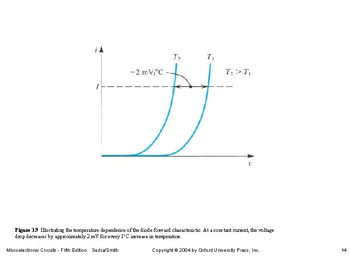
Figure 3. 9 Illustrating the temperature dependence of the diode forward characteristic. At a constant current, the voltage drop decreases by approximately 2 m. V for every 1 C increase in temperature. Microelectronic Circuits - Fifth Edition Sedra/Smith Copyright 2004 by Oxford University Press, Inc. 14

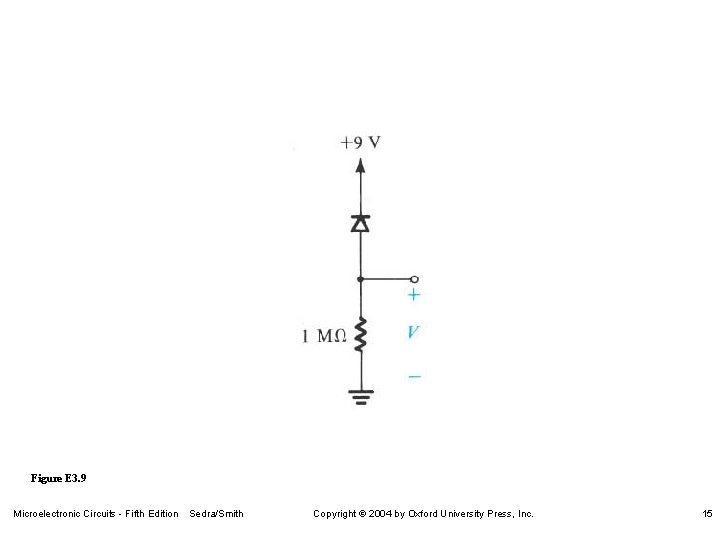
Figure E 3. 9 Microelectronic Circuits - Fifth Edition Sedra/Smith Copyright 2004 by Oxford University Press, Inc. 15

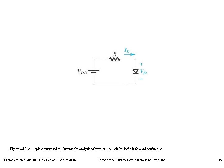
Figure 3. 10 A simple circuit used to illustrate the analysis of circuits in which the diode is forward conducting. Microelectronic Circuits - Fifth Edition Sedra/Smith Copyright 2004 by Oxford University Press, Inc. 16

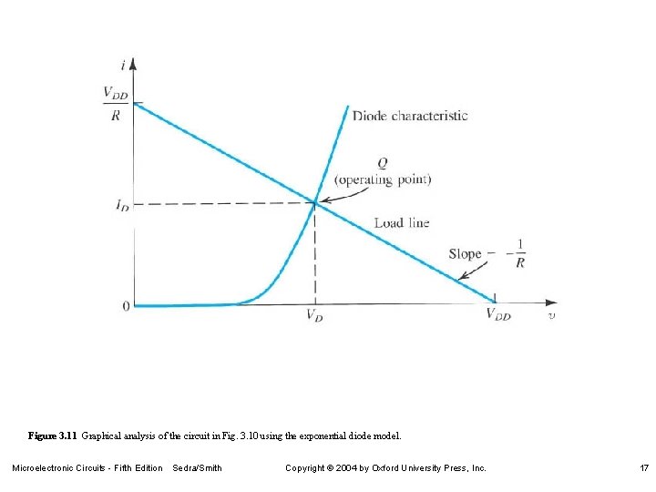
Figure 3. 11 Graphical analysis of the circuit in Fig. 3. 10 using the exponential diode model. Microelectronic Circuits - Fifth Edition Sedra/Smith Copyright 2004 by Oxford University Press, Inc. 17

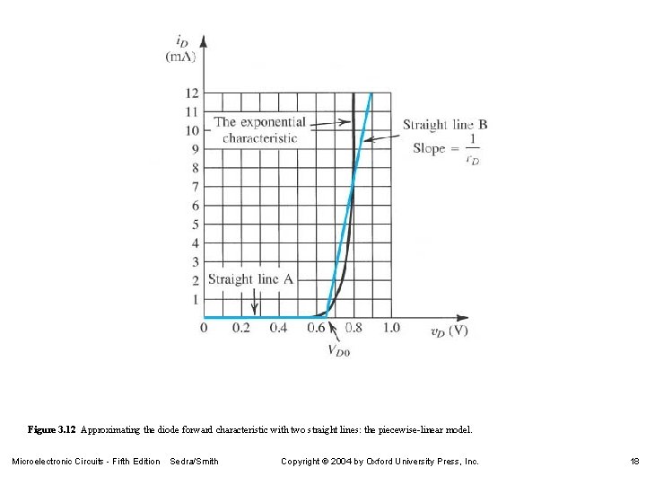
Figure 3. 12 Approximating the diode forward characteristic with two straight lines: the piecewise-linear model. Microelectronic Circuits - Fifth Edition Sedra/Smith Copyright 2004 by Oxford University Press, Inc. 18

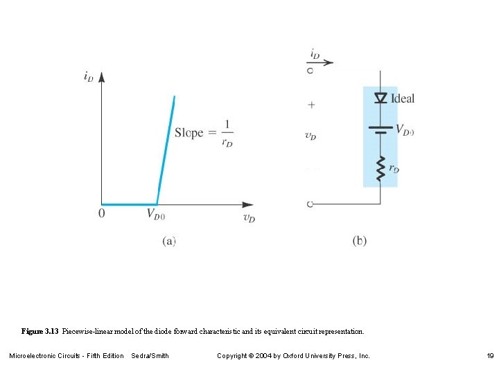
Figure 3. 13 Piecewise-linear model of the diode forward characteristic and its equivalent circuit representation. Microelectronic Circuits - Fifth Edition Sedra/Smith Copyright 2004 by Oxford University Press, Inc. 19

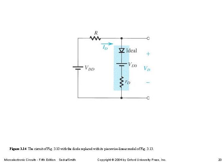
Figure 3. 14 The circuit of Fig. 3. 10 with the diode replaced with its piecewise-linear model of Fig. 3. 13. Microelectronic Circuits - Fifth Edition Sedra/Smith Copyright 2004 by Oxford University Press, Inc. 20

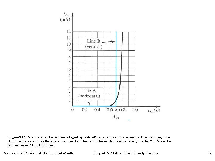
Figure 3. 15 Development of the constant-voltage-drop model of the diode forward characteristics. A vertical straight line (B) is used to approximate the fast-rising exponential. Observe that this simple model predicts VD to within 0. 1 V over the current range of 0. 1 m. A to 10 m. A. Microelectronic Circuits - Fifth Edition Sedra/Smith Copyright 2004 by Oxford University Press, Inc. 21

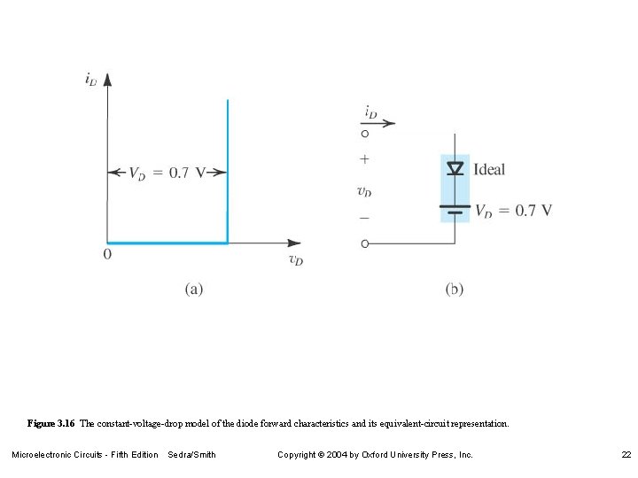
Figure 3. 16 The constant-voltage-drop model of the diode forward characteristics and its equivalent-circuit representation. Microelectronic Circuits - Fifth Edition Sedra/Smith Copyright 2004 by Oxford University Press, Inc. 22

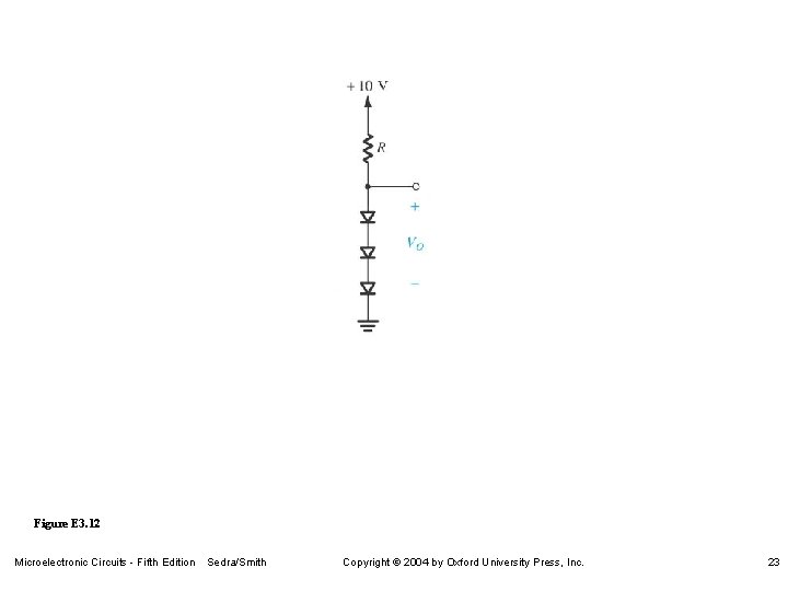
Figure E 3. 12 Microelectronic Circuits - Fifth Edition Sedra/Smith Copyright 2004 by Oxford University Press, Inc. 23

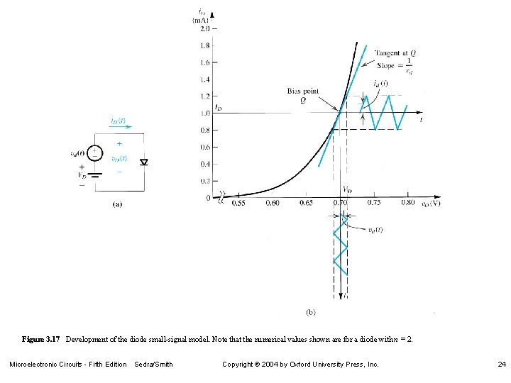
Figure 3. 17 Development of the diode small-signal model. Note that the numerical values shown are for a diode with n = 2. Microelectronic Circuits - Fifth Edition Sedra/Smith Copyright 2004 by Oxford University Press, Inc. 24

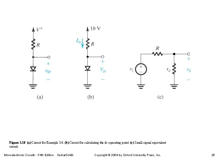
Figure 3. 18 (a) Circuit for Example 3. 6. (b) Circuit for calculating the dc operating point. (c) Small-signal equivalent circuit. Microelectronic Circuits - Fifth Edition Sedra/Smith Copyright 2004 by Oxford University Press, Inc. 25

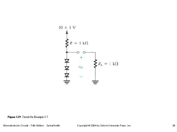
Figure 3. 19 Circuit for Example 3. 7. Microelectronic Circuits - Fifth Edition Sedra/Smith Copyright 2004 by Oxford University Press, Inc. 26

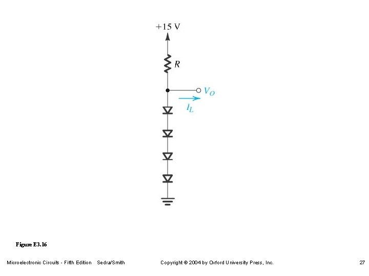
Figure E 3. 16 Microelectronic Circuits - Fifth Edition Sedra/Smith Copyright 2004 by Oxford University Press, Inc. 27

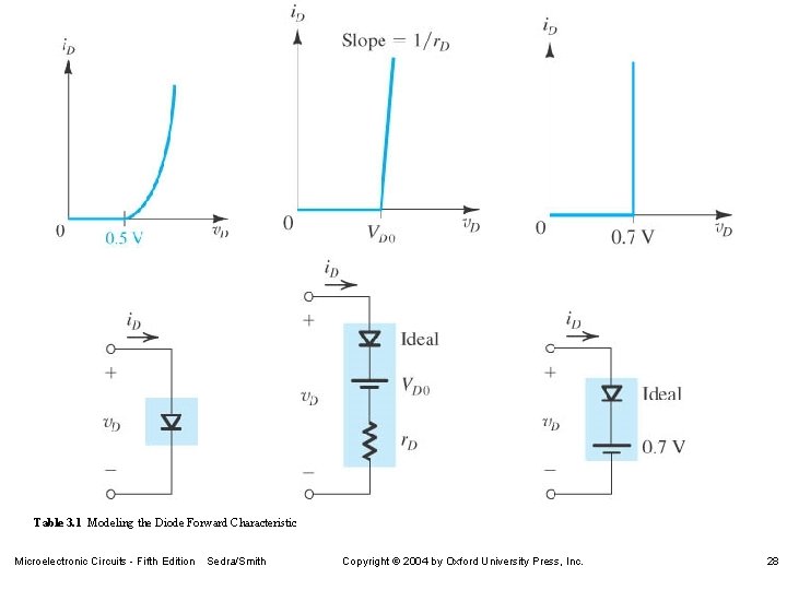
Table 3. 1 Modeling the Diode Forward Characteristic Microelectronic Circuits - Fifth Edition Sedra/Smith Copyright 2004 by Oxford University Press, Inc. 28

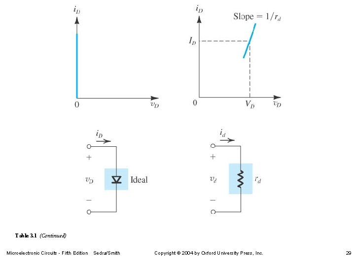
Table 3. 1 (Continued) Microelectronic Circuits - Fifth Edition Sedra/Smith Copyright 2004 by Oxford University Press, Inc. 29

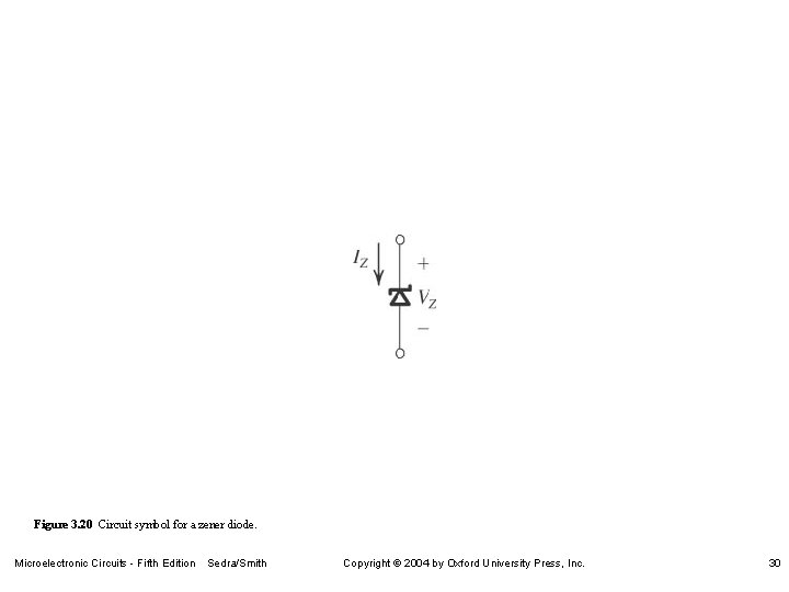
Figure 3. 20 Circuit symbol for a zener diode. Microelectronic Circuits - Fifth Edition Sedra/Smith Copyright 2004 by Oxford University Press, Inc. 30

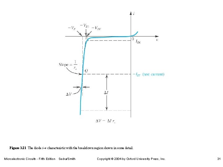
Figure 3. 21 The diode i–v characteristic with the breakdown region shown in some detail. Microelectronic Circuits - Fifth Edition Sedra/Smith Copyright 2004 by Oxford University Press, Inc. 31

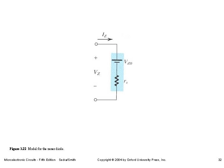
Figure 3. 22 Model for the zener diode. Microelectronic Circuits - Fifth Edition Sedra/Smith Copyright 2004 by Oxford University Press, Inc. 32

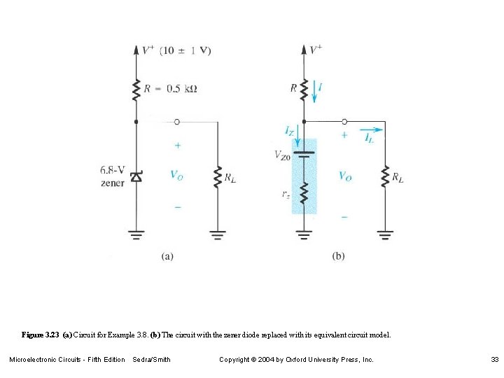
Figure 3. 23 (a) Circuit for Example 3. 8. (b) The circuit with the zener diode replaced with its equivalent circuit model. Microelectronic Circuits - Fifth Edition Sedra/Smith Copyright 2004 by Oxford University Press, Inc. 33

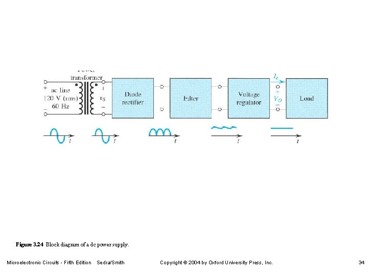
Figure 3. 24 Block diagram of a dc power supply. Microelectronic Circuits - Fifth Edition Sedra/Smith Copyright 2004 by Oxford University Press, Inc. 34

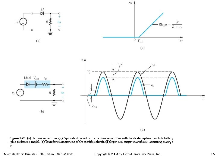
Figure 3. 25 (a) Half-wave rectifier. (b) Equivalent circuit of the half-wave rectifier with the diode replaced with its battery -plus-resistance model. (c) Transfer characteristic of the rectifier circuit. (d) Input and output waveforms, assuming that r. D ! R. Microelectronic Circuits - Fifth Edition Sedra/Smith Copyright 2004 by Oxford University Press, Inc. 35

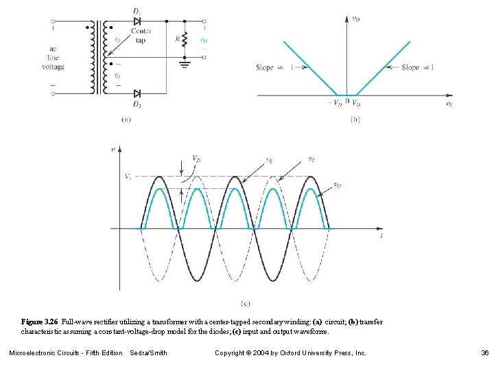
Figure 3. 26 Full-wave rectifier utilizing a transformer with a center-tapped secondary winding: (a) circuit; (b) transfer characteristic assuming a constant-voltage-drop model for the diodes; (c) input and output waveforms. Microelectronic Circuits - Fifth Edition Sedra/Smith Copyright 2004 by Oxford University Press, Inc. 36

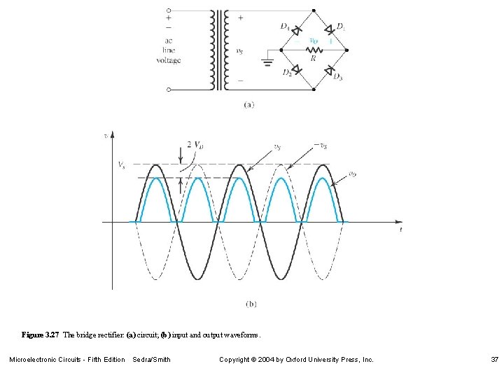
Figure 3. 27 The bridge rectifier: (a) circuit; (b) input and output waveforms. Microelectronic Circuits - Fifth Edition Sedra/Smith Copyright 2004 by Oxford University Press, Inc. 37

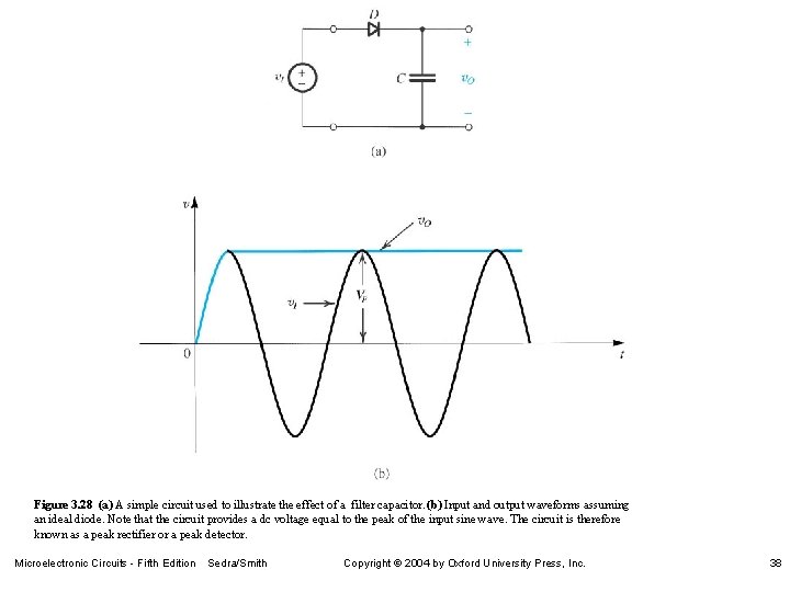
Figure 3. 28 (a) A simple circuit used to illustrate the effect of a filter capacitor. (b) Input and output waveforms assuming an ideal diode. Note that the circuit provides a dc voltage equal to the peak of the input sine wave. The circuit is therefore known as a peak rectifier or a peak detector. Microelectronic Circuits - Fifth Edition Sedra/Smith Copyright 2004 by Oxford University Press, Inc. 38

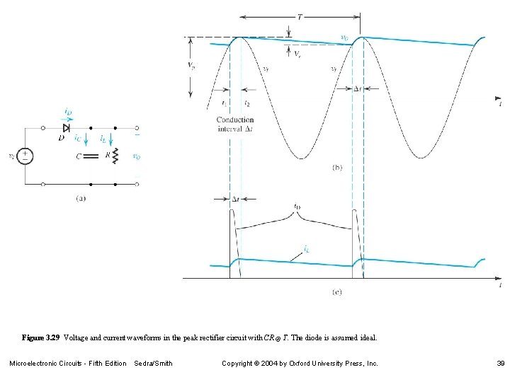
Figure 3. 29 Voltage and current waveforms in the peak rectifier circuit with CR @ T. The diode is assumed ideal. Microelectronic Circuits - Fifth Edition Sedra/Smith Copyright 2004 by Oxford University Press, Inc. 39

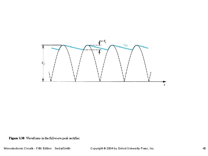
Figure 3. 30 Waveforms in the full-wave peak rectifier. Microelectronic Circuits - Fifth Edition Sedra/Smith Copyright 2004 by Oxford University Press, Inc. 40

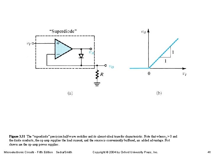
Figure 3. 31 The “superdiode” precision half-wave rectifier and its almost-ideal transfer characteristic. Note that when v. I > 0 and the diode conducts, the op amp supplies the load current, and the source is conveniently buffered, an added advantage. Not shown are the op-amp power supplies. Microelectronic Circuits - Fifth Edition Sedra/Smith Copyright 2004 by Oxford University Press, Inc. 41

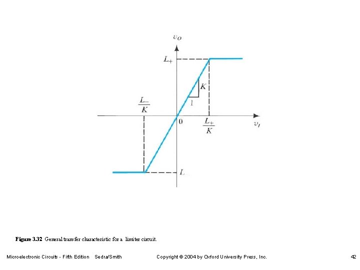
Figure 3. 32 General transfer characteristic for a limiter circuit. Microelectronic Circuits - Fifth Edition Sedra/Smith Copyright 2004 by Oxford University Press, Inc. 42

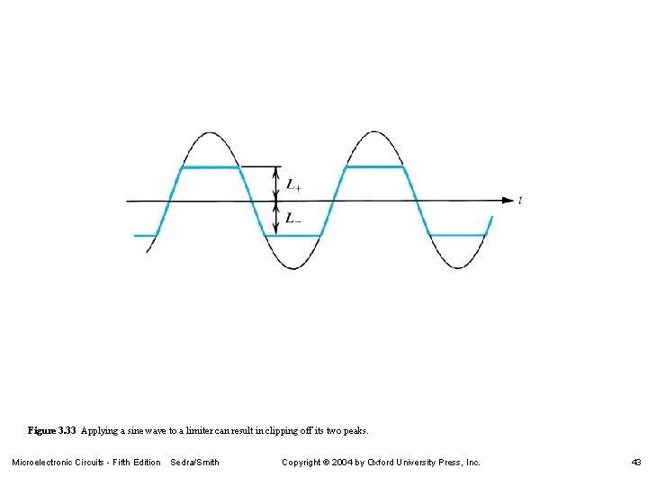
Figure 3. 33 Applying a sine wave to a limiter can result in clipping off its two peaks. Microelectronic Circuits - Fifth Edition Sedra/Smith Copyright 2004 by Oxford University Press, Inc. 43

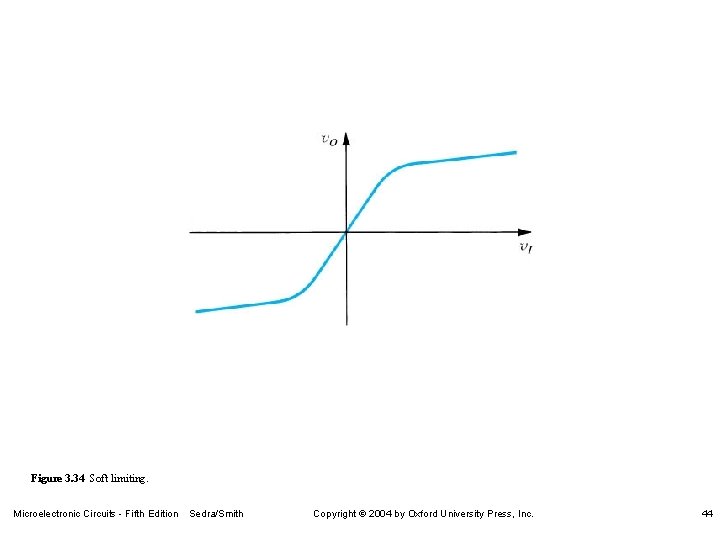
Figure 3. 34 Soft limiting. Microelectronic Circuits - Fifth Edition Sedra/Smith Copyright 2004 by Oxford University Press, Inc. 44

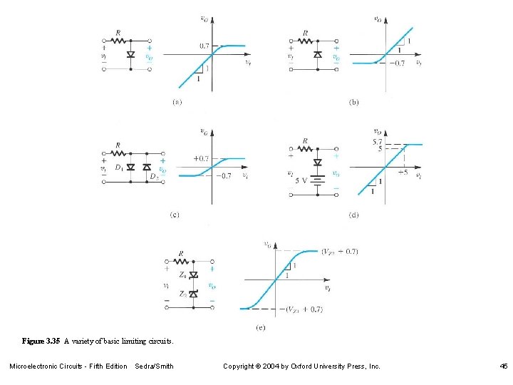
Figure 3. 35 A variety of basic limiting circuits. Microelectronic Circuits - Fifth Edition Sedra/Smith Copyright 2004 by Oxford University Press, Inc. 45

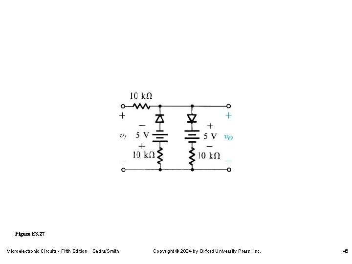
Figure E 3. 27 Microelectronic Circuits - Fifth Edition Sedra/Smith Copyright 2004 by Oxford University Press, Inc. 46

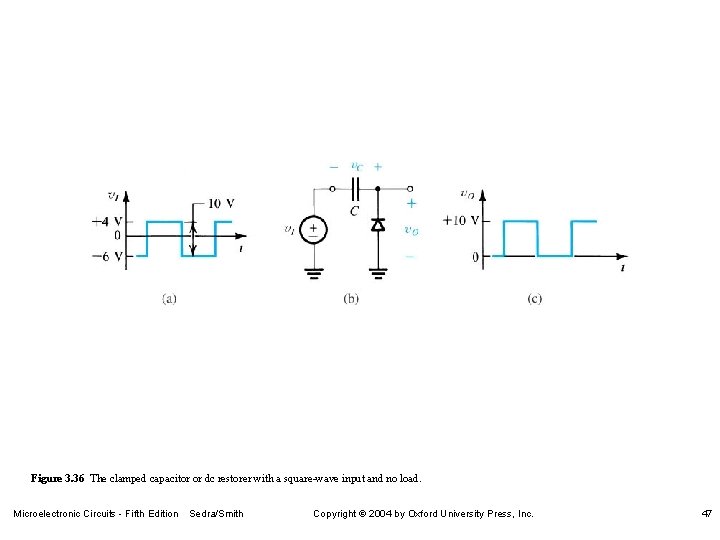
Figure 3. 36 The clamped capacitor or dc restorer with a square-wave input and no load. Microelectronic Circuits - Fifth Edition Sedra/Smith Copyright 2004 by Oxford University Press, Inc. 47

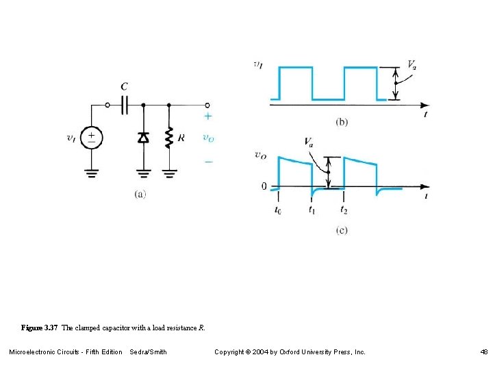
Figure 3. 37 The clamped capacitor with a load resistance R. Microelectronic Circuits - Fifth Edition Sedra/Smith Copyright 2004 by Oxford University Press, Inc. 48

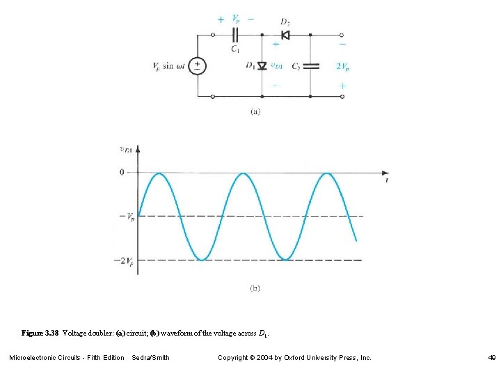
Figure 3. 38 Voltage doubler: (a) circuit; (b) waveform of the voltage across D 1. Microelectronic Circuits - Fifth Edition Sedra/Smith Copyright 2004 by Oxford University Press, Inc. 49

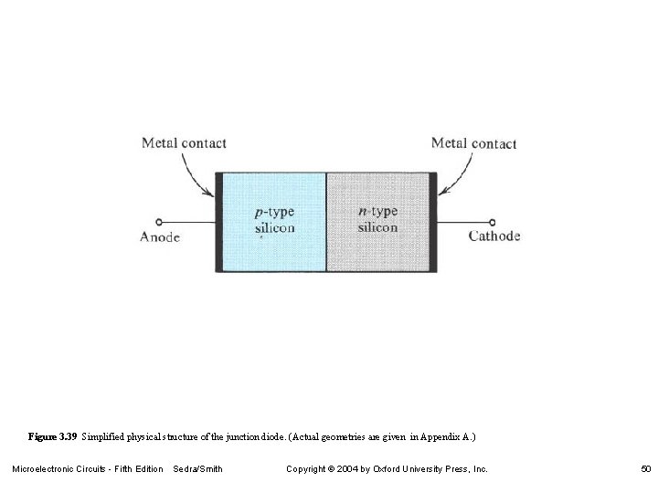
Figure 3. 39 Simplified physical structure of the junction diode. (Actual geometries are given in Appendix A. ) Microelectronic Circuits - Fifth Edition Sedra/Smith Copyright 2004 by Oxford University Press, Inc. 50

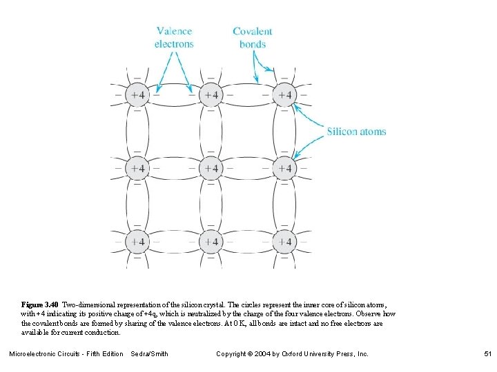
Figure 3. 40 Two-dimensional representation of the silicon crystal. The circles represent the inner core of silicon atoms, with +4 indicating its positive charge of +4 q, which is neutralized by the charge of the four valence electrons. Observe how the covalent bonds are formed by sharing of the valence electrons. At 0 K, all bonds are intact and no free electrons are available for current conduction. Microelectronic Circuits - Fifth Edition Sedra/Smith Copyright 2004 by Oxford University Press, Inc. 51

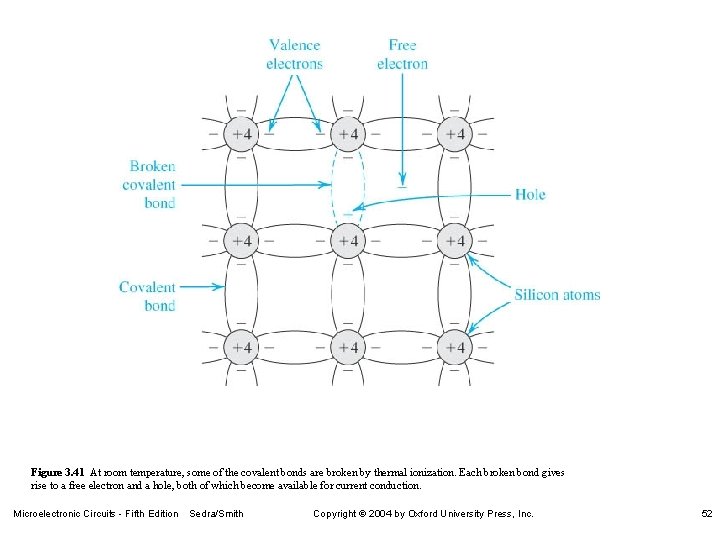
Figure 3. 41 At room temperature, some of the covalent bonds are broken by thermal ionization. Each broken bond gives rise to a free electron and a hole, both of which become available for current conduction. Microelectronic Circuits - Fifth Edition Sedra/Smith Copyright 2004 by Oxford University Press, Inc. 52

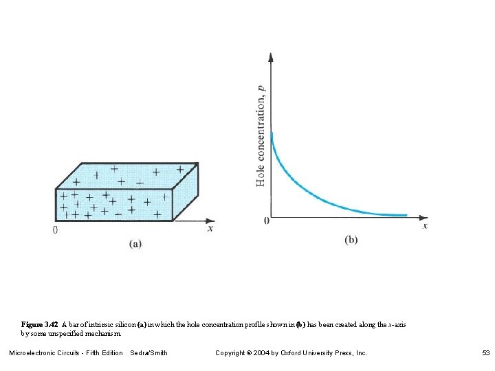
Figure 3. 42 A bar of intrinsic silicon (a) in which the hole concentration profile shown in (b) has been created along the x-axis by some unspecified mechanism. Microelectronic Circuits - Fifth Edition Sedra/Smith Copyright 2004 by Oxford University Press, Inc. 53

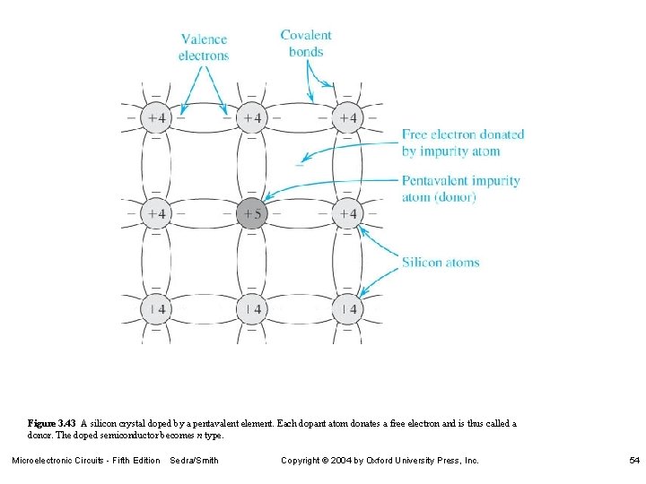
Figure 3. 43 A silicon crystal doped by a pentavalent element. Each dopant atom donates a free electron and is thus called a donor. The doped semiconductor becomes n type. Microelectronic Circuits - Fifth Edition Sedra/Smith Copyright 2004 by Oxford University Press, Inc. 54

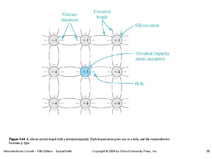
Figure 3. 44 A silicon crystal doped with a trivalent impurity. Each dopant atom gives rise to a hole, and the semiconductor becomes p type. Microelectronic Circuits - Fifth Edition Sedra/Smith Copyright 2004 by Oxford University Press, Inc. 55

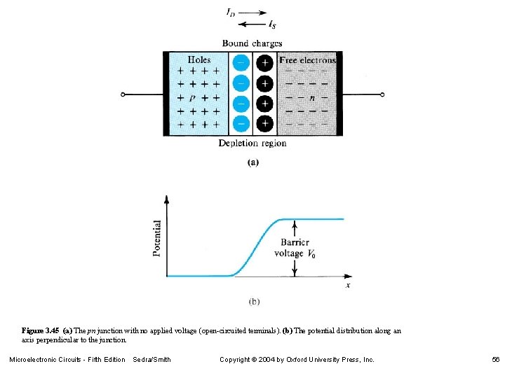
Figure 3. 45 (a) The pn junction with no applied voltage (open-circuited terminals). (b) The potential distribution along an axis perpendicular to the junction. Microelectronic Circuits - Fifth Edition Sedra/Smith Copyright 2004 by Oxford University Press, Inc. 56

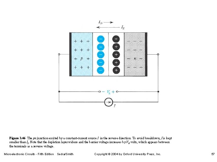
Figure 3. 46 The pn junction excited by a constant-current source I in the reverse direction. To avoid breakdown, I is kept smaller than IS. Note that the depletion layer widens and the barrier voltage increases by VR volts, which appears between the terminals as a reverse voltage. Microelectronic Circuits - Fifth Edition Sedra/Smith Copyright 2004 by Oxford University Press, Inc. 57

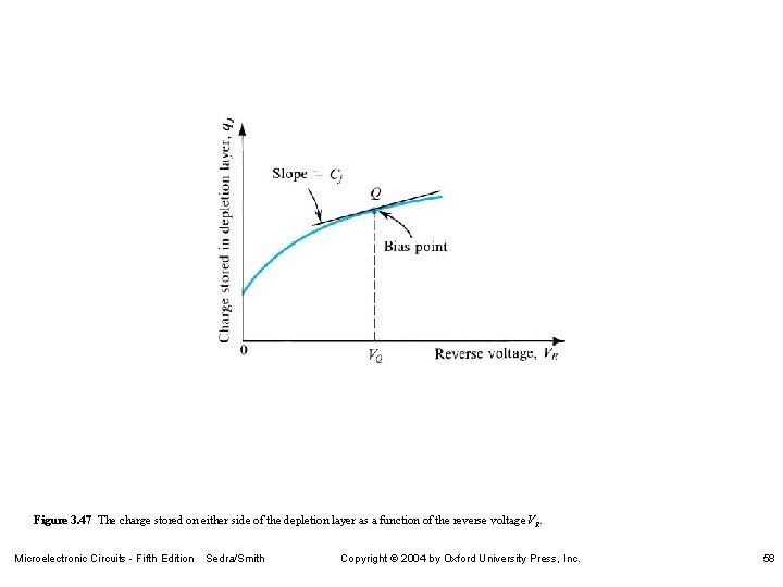
Figure 3. 47 The charge stored on either side of the depletion layer as a function of the reverse voltage VR. Microelectronic Circuits - Fifth Edition Sedra/Smith Copyright 2004 by Oxford University Press, Inc. 58

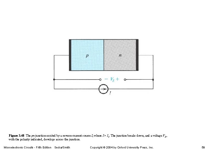
Figure 3. 48 The pn junction excited by a reverse-current source I, where I > IS. The junction breaks down, and a voltage VZ , with the polarity indicated, develops across the junction. Microelectronic Circuits - Fifth Edition Sedra/Smith Copyright 2004 by Oxford University Press, Inc. 59

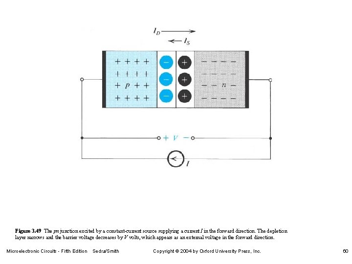
Figure 3. 49 The pn junction excited by a constant-current source supplying a current I in the forward direction. The depletion layer narrows and the barrier voltage decreases by V volts, which appears as an external voltage in the forward direction. Microelectronic Circuits - Fifth Edition Sedra/Smith Copyright 2004 by Oxford University Press, Inc. 60

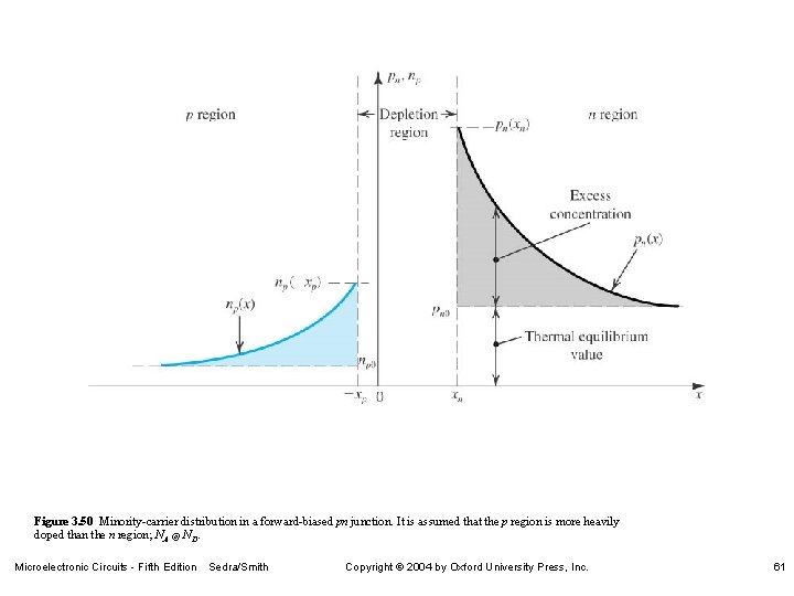
Figure 3. 50 Minority-carrier distribution in a forward-biased pn junction. It is assumed that the p region is more heavily doped than the n region; NA @ ND. Microelectronic Circuits - Fifth Edition Sedra/Smith Copyright 2004 by Oxford University Press, Inc. 61

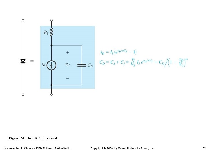
Figure 3. 51 The SPICE diode model. Microelectronic Circuits - Fifth Edition Sedra/Smith Copyright 2004 by Oxford University Press, Inc. 62

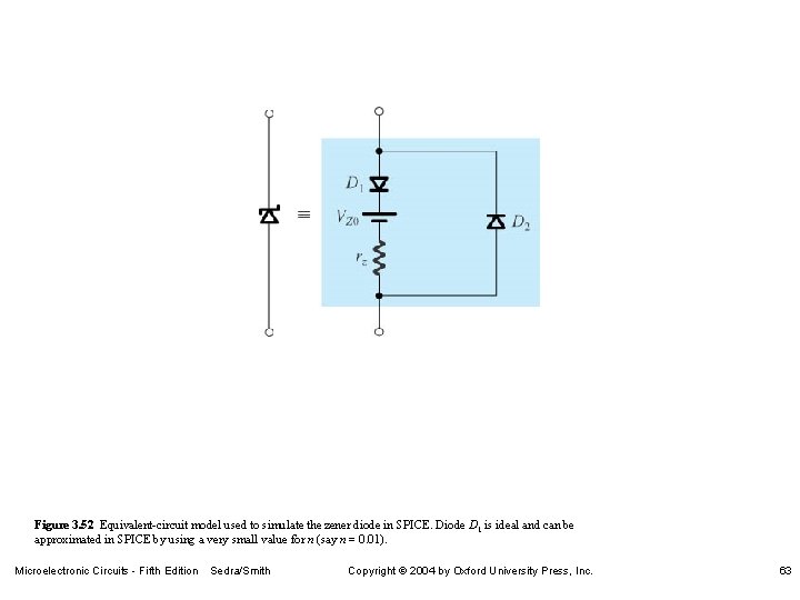
Figure 3. 52 Equivalent-circuit model used to simulate the zener diode in SPICE. Diode D 1 is ideal and can be approximated in SPICE by using a very small value for n (say n = 0. 01). Microelectronic Circuits - Fifth Edition Sedra/Smith Copyright 2004 by Oxford University Press, Inc. 63

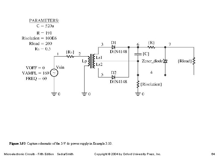
Figure 3. 53 Capture schematic of the 5 -V dc power supply in Example 3. 10. Microelectronic Circuits - Fifth Edition Sedra/Smith Copyright 2004 by Oxford University Press, Inc. 64

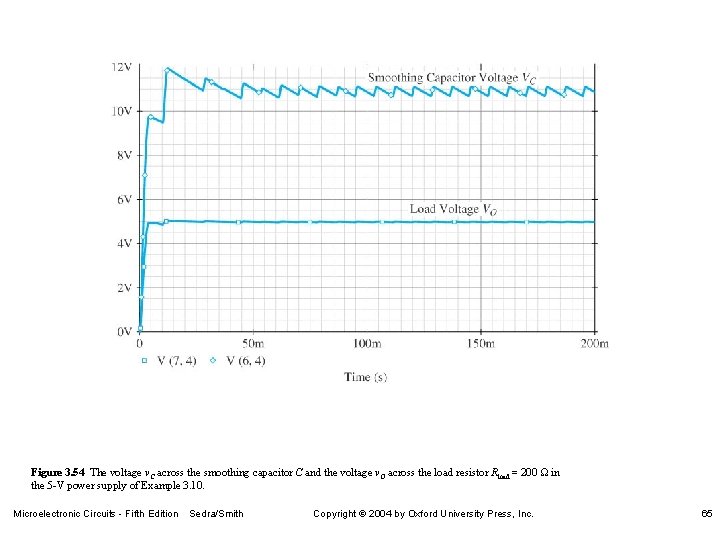
Figure 3. 54 The voltage v. C across the smoothing capacitor C and the voltage v. O across the load resistor Rload = 200 in the 5 -V power supply of Example 3. 10. Microelectronic Circuits - Fifth Edition Sedra/Smith Copyright 2004 by Oxford University Press, Inc. 65

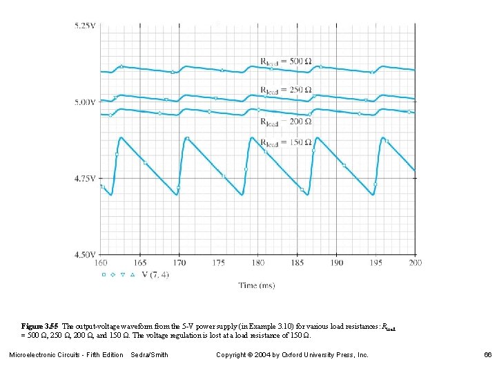
Figure 3. 55 The output-voltage waveform from the 5 -V power supply (in Example 3. 10) for various load resistances: Rload = 500 , 250 , 200 , and 150 . The voltage regulation is lost at a load resistance of 150 . Microelectronic Circuits - Fifth Edition Sedra/Smith Copyright 2004 by Oxford University Press, Inc. 66

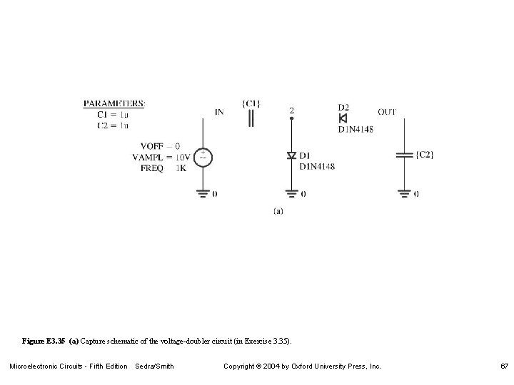
Figure E 3. 35 (a) Capture schematic of the voltage-doubler circuit (in Exercise 3. 35). Microelectronic Circuits - Fifth Edition Sedra/Smith Copyright 2004 by Oxford University Press, Inc. 67

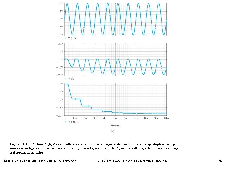
Figure E 3. 35 (Continued) (b) Various voltage waveforms in the voltage-doubler circuit. The top graph displays the input sine-wave voltage signal, the middle graph displays the voltage across diode D 1, and the bottom graph displays the voltage that appears at the output. Microelectronic Circuits - Fifth Edition Sedra/Smith Copyright 2004 by Oxford University Press, Inc. 68

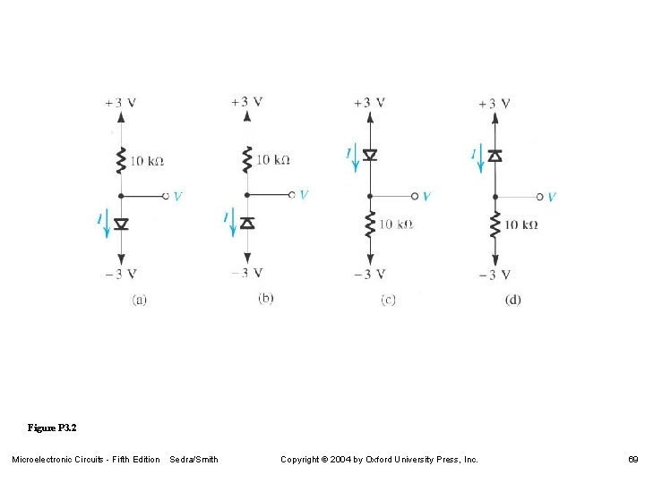
Figure P 3. 2 Microelectronic Circuits - Fifth Edition Sedra/Smith Copyright 2004 by Oxford University Press, Inc. 69

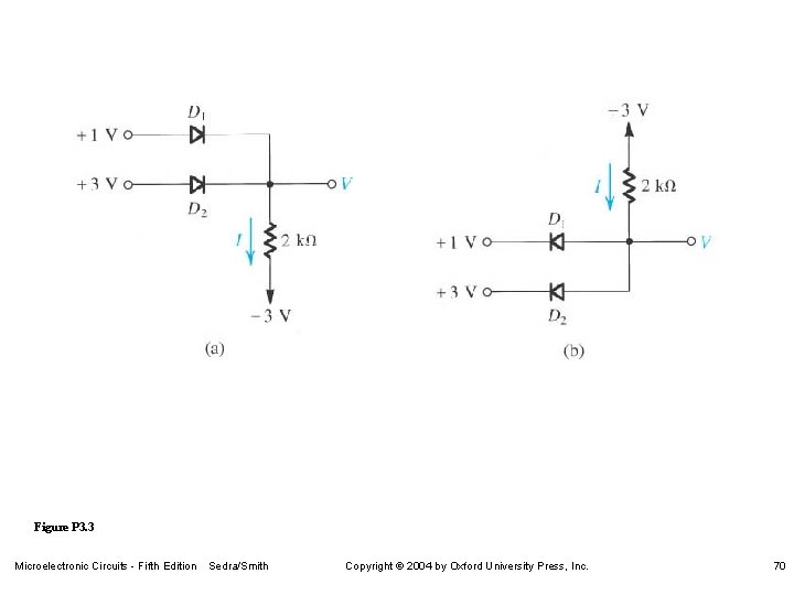
Figure P 3. 3 Microelectronic Circuits - Fifth Edition Sedra/Smith Copyright 2004 by Oxford University Press, Inc. 70

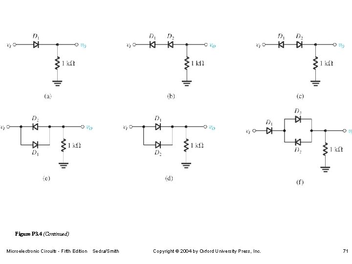
Figure P 3. 4 (Continued) Microelectronic Circuits - Fifth Edition Sedra/Smith Copyright 2004 by Oxford University Press, Inc. 71

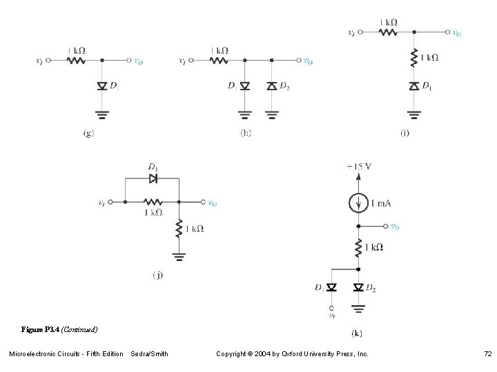
Figure P 3. 4 (Continued) Microelectronic Circuits - Fifth Edition Sedra/Smith Copyright 2004 by Oxford University Press, Inc. 72

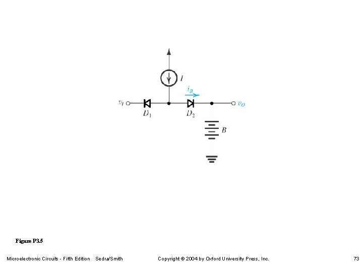
Figure P 3. 5 Microelectronic Circuits - Fifth Edition Sedra/Smith Copyright 2004 by Oxford University Press, Inc. 73

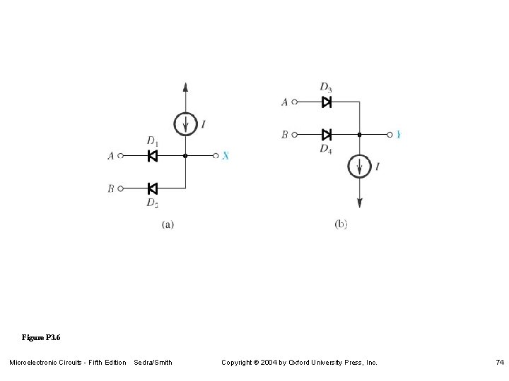
Figure P 3. 6 Microelectronic Circuits - Fifth Edition Sedra/Smith Copyright 2004 by Oxford University Press, Inc. 74

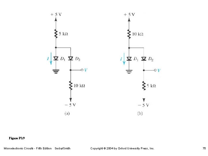
Figure P 3. 9 Microelectronic Circuits - Fifth Edition Sedra/Smith Copyright 2004 by Oxford University Press, Inc. 75

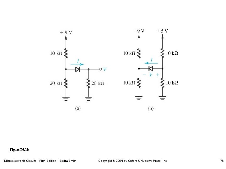
Figure P 3. 10 Microelectronic Circuits - Fifth Edition Sedra/Smith Copyright 2004 by Oxford University Press, Inc. 76

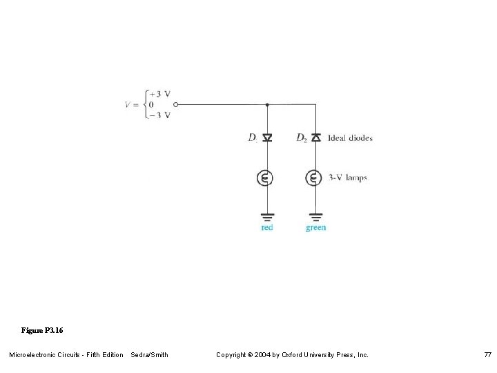
Figure P 3. 16 Microelectronic Circuits - Fifth Edition Sedra/Smith Copyright 2004 by Oxford University Press, Inc. 77

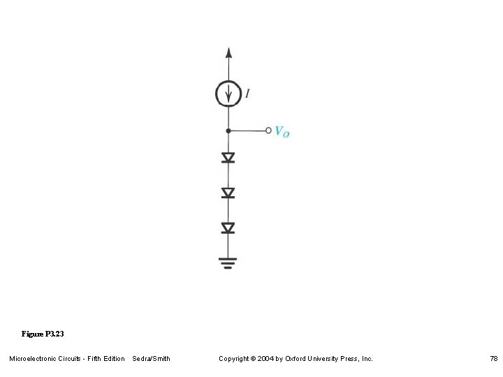
Figure P 3. 23 Microelectronic Circuits - Fifth Edition Sedra/Smith Copyright 2004 by Oxford University Press, Inc. 78

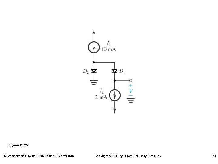
Figure P 3. 25 Microelectronic Circuits - Fifth Edition Sedra/Smith Copyright 2004 by Oxford University Press, Inc. 79

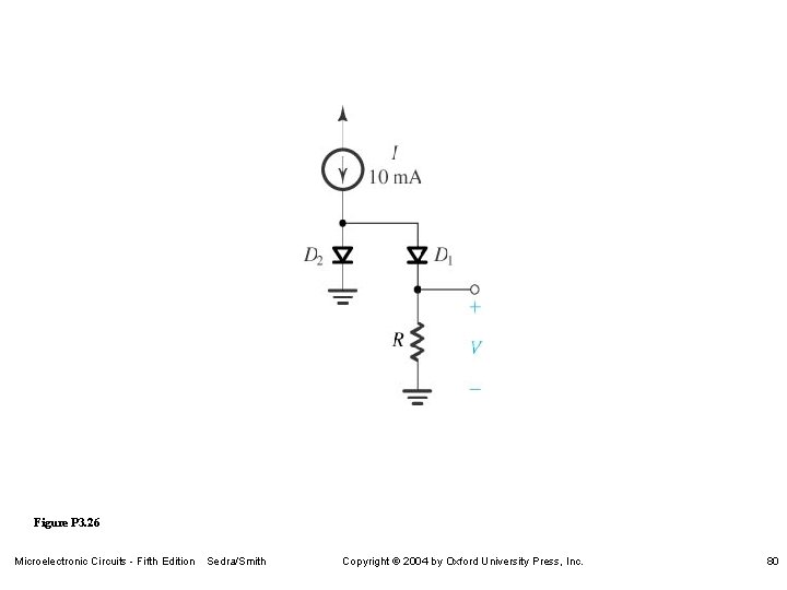
Figure P 3. 26 Microelectronic Circuits - Fifth Edition Sedra/Smith Copyright 2004 by Oxford University Press, Inc. 80

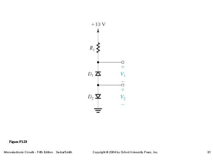
Figure P 3. 28 Microelectronic Circuits - Fifth Edition Sedra/Smith Copyright 2004 by Oxford University Press, Inc. 81

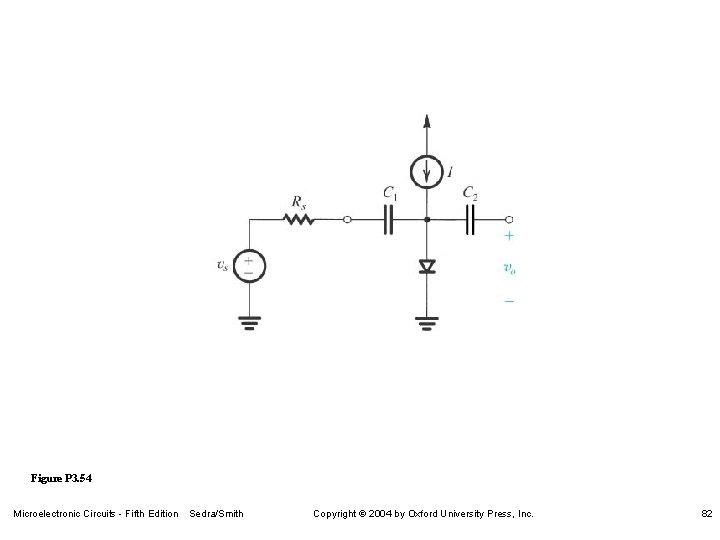
Figure P 3. 54 Microelectronic Circuits - Fifth Edition Sedra/Smith Copyright 2004 by Oxford University Press, Inc. 82

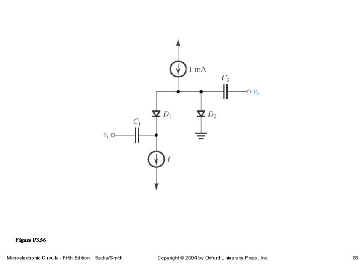
Figure P 3. 56 Microelectronic Circuits - Fifth Edition Sedra/Smith Copyright 2004 by Oxford University Press, Inc. 83

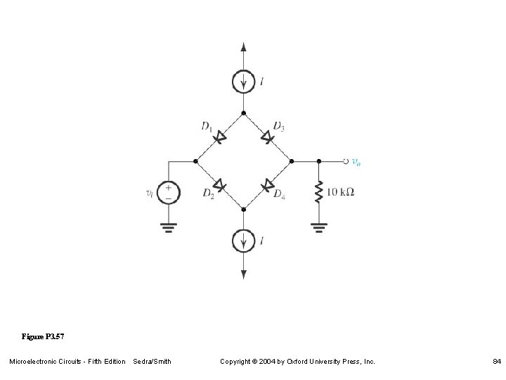
Figure P 3. 57 Microelectronic Circuits - Fifth Edition Sedra/Smith Copyright 2004 by Oxford University Press, Inc. 84

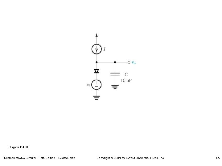
Figure P 3. 58 Microelectronic Circuits - Fifth Edition Sedra/Smith Copyright 2004 by Oxford University Press, Inc. 85

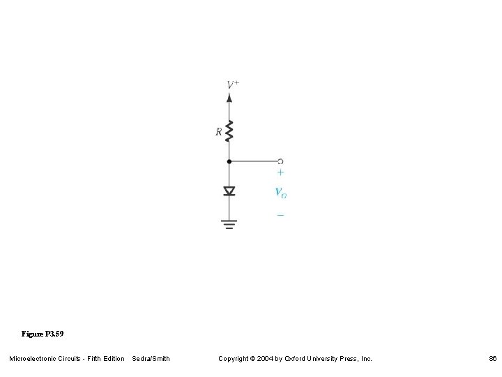
Figure P 3. 59 Microelectronic Circuits - Fifth Edition Sedra/Smith Copyright 2004 by Oxford University Press, Inc. 86

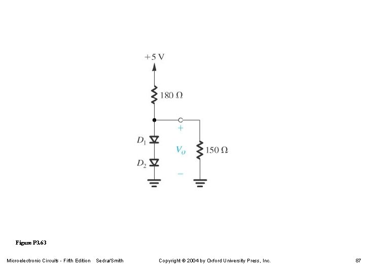
Figure P 3. 63 Microelectronic Circuits - Fifth Edition Sedra/Smith Copyright 2004 by Oxford University Press, Inc. 87

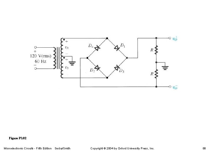
Figure P 3. 82 Microelectronic Circuits - Fifth Edition Sedra/Smith Copyright 2004 by Oxford University Press, Inc. 88

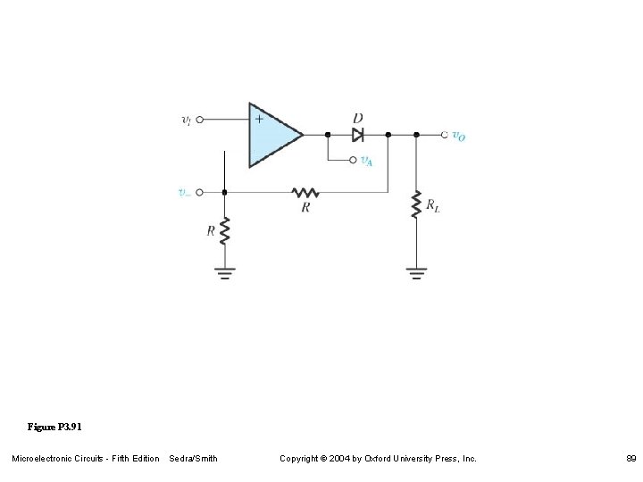
Figure P 3. 91 Microelectronic Circuits - Fifth Edition Sedra/Smith Copyright 2004 by Oxford University Press, Inc. 89

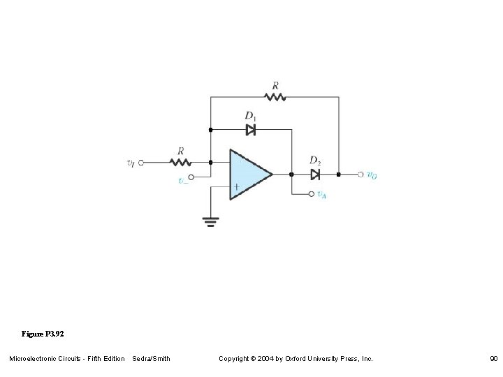
Figure P 3. 92 Microelectronic Circuits - Fifth Edition Sedra/Smith Copyright 2004 by Oxford University Press, Inc. 90

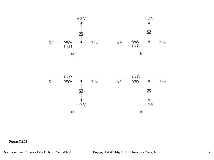
Figure P 3. 93 Microelectronic Circuits - Fifth Edition Sedra/Smith Copyright 2004 by Oxford University Press, Inc. 91

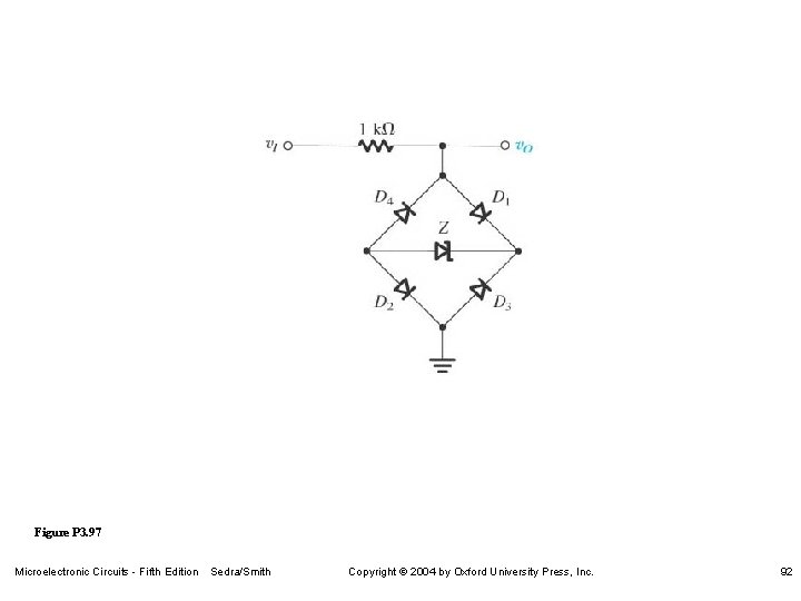
Figure P 3. 97 Microelectronic Circuits - Fifth Edition Sedra/Smith Copyright 2004 by Oxford University Press, Inc. 92

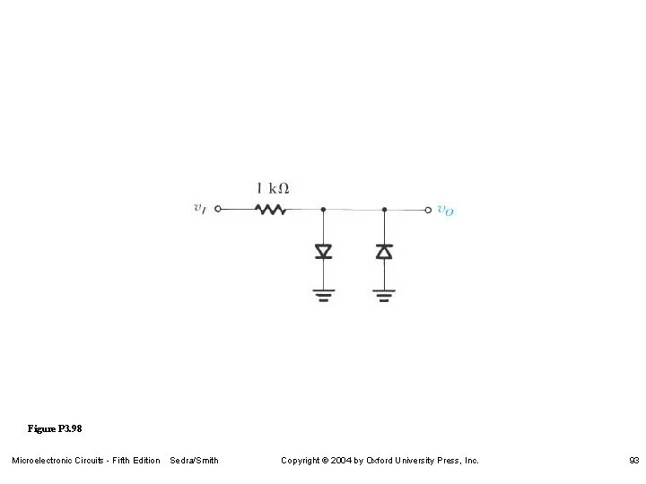
Figure P 3. 98 Microelectronic Circuits - Fifth Edition Sedra/Smith Copyright 2004 by Oxford University Press, Inc. 93

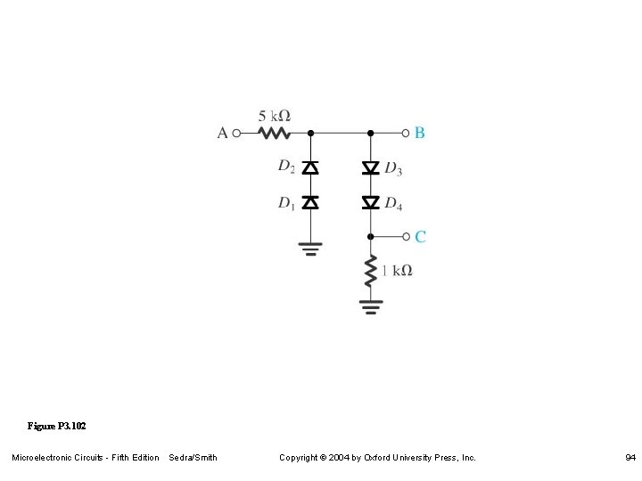
Figure P 3. 102 Microelectronic Circuits - Fifth Edition Sedra/Smith Copyright 2004 by Oxford University Press, Inc. 94

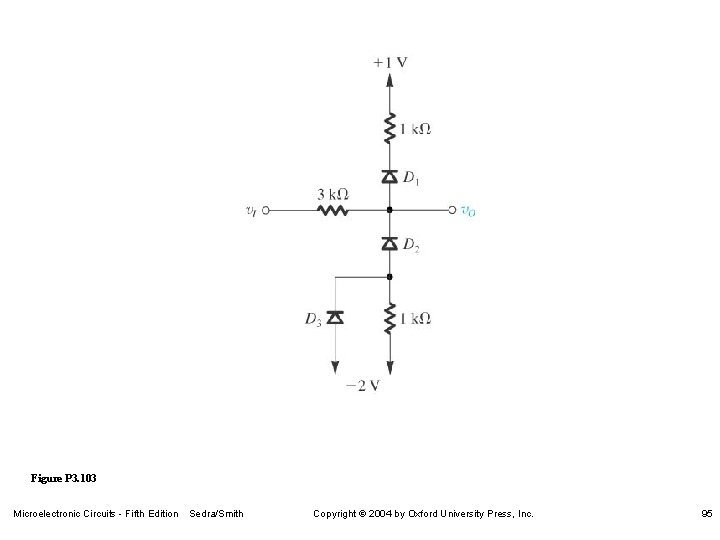
Figure P 3. 103 Microelectronic Circuits - Fifth Edition Sedra/Smith Copyright 2004 by Oxford University Press, Inc. 95

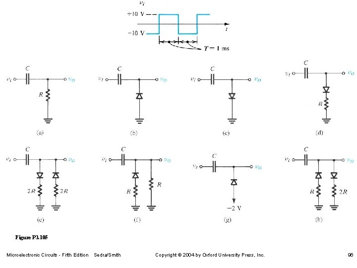
Figure P 3. 105 Microelectronic Circuits - Fifth Edition Sedra/Smith Copyright 2004 by Oxford University Press, Inc. 96

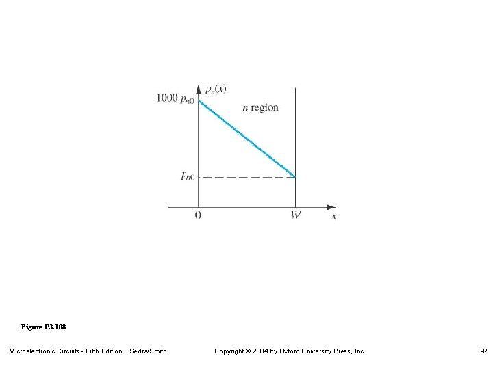
Figure P 3. 108 Microelectronic Circuits - Fifth Edition Sedra/Smith Copyright 2004 by Oxford University Press, Inc. 97