Digital CMOS Logic Circuits CMOS digital circuits small
- Slides: 10

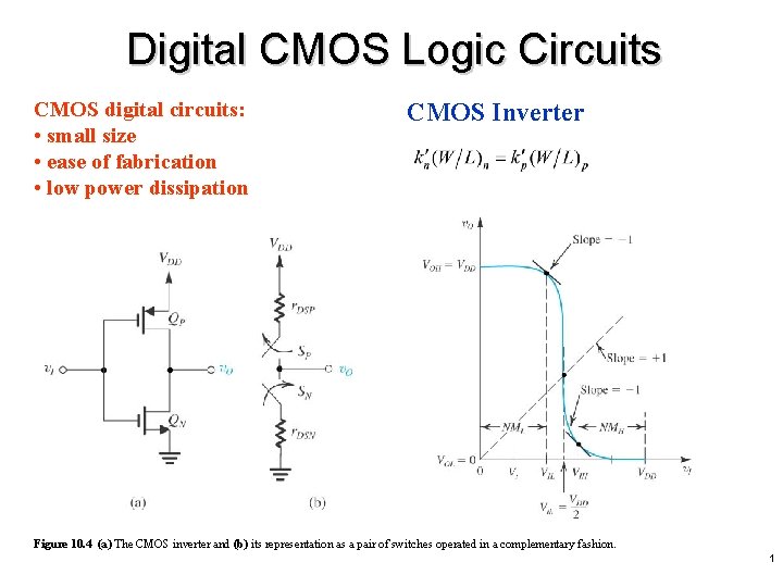
Digital CMOS Logic Circuits CMOS digital circuits: • small size • ease of fabrication • low power dissipation CMOS Inverter Figure 10. 4 (a) The CMOS inverter and (b) its representation as a pair of switches operated in a complementary fashion. 1

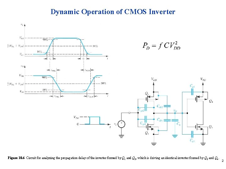
Dynamic Operation of CMOS Inverter Figure 10. 6 Circuit for analyzing the propagation delay of the inverter formed by Q 1 and Q 2, which is driving an identical inverter formed by Q 3 and Q 4. 2

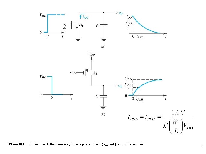
Figure 10. 7 Equivalent circuits for determining the propagation delays (a) t. PHL and (b) t. PLH of the inverter. 3

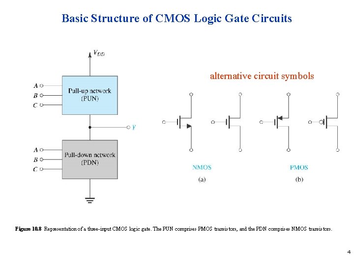
Basic Structure of CMOS Logic Gate Circuits alternative circuit symbols Figure 10. 8 Representation of a three-input CMOS logic gate. The PUN comprises PMOS transistors, and the PDN comprises NMOS transistors. 4

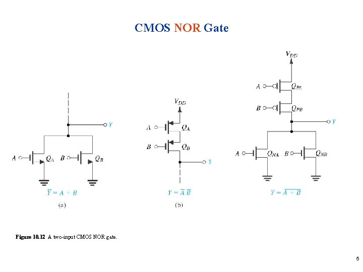
CMOS NOR Gate Figure 10. 12 A two-input CMOS NOR gate. 5

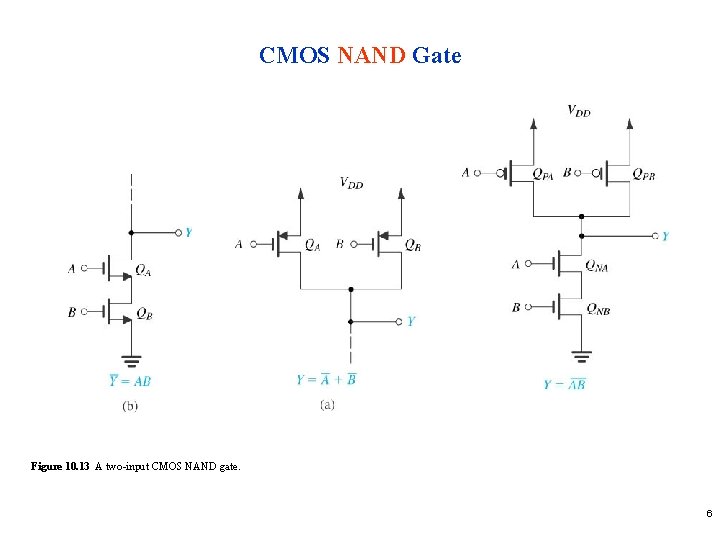
CMOS NAND Gate Figure 10. 13 A two-input CMOS NAND gate. 6

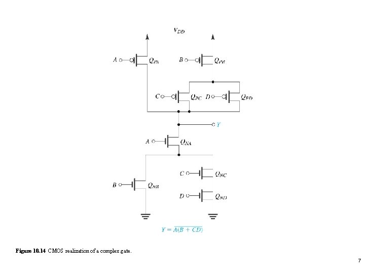
Figure 10. 14 CMOS realization of a complex gate. 7

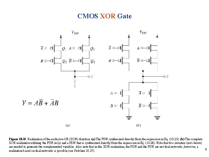
CMOS XOR Gate Figure 10. 15 Realization of the exclusive-OR (XOR) function: (a) The PUN synthesized directly from the expression in Eq. (10. 25). (b) The complete XOR realization utilizing the PUN in (a) and a PDN that is synthesized directly from the expression in Eq. (10. 26). Note that two inverters (not shown) are needed to generate the complemented variables. Also note that in this XOR realization, the PDN and the PUN are not dual networks; however, a 8 realization based on dual networks is possible (see Problem 10. 27).

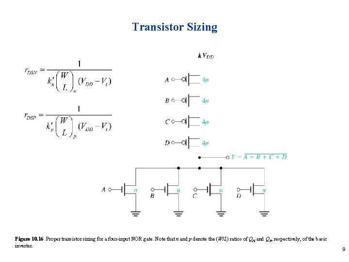
Transistor Sizing Figure 10. 16 Proper transistor sizing for a four-input NOR gate. Note that n and p denote the (W/L) ratios of QN and QP, respectively, of the basic inverter. 9

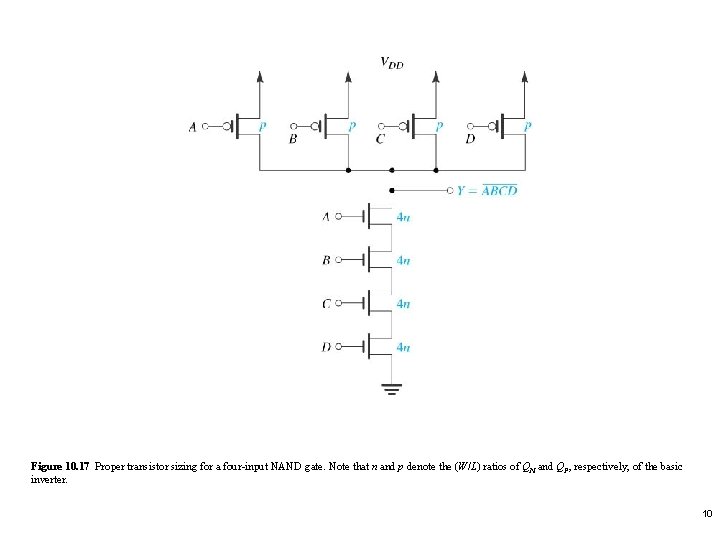
Figure 10. 17 Proper transistor sizing for a four-input NAND gate. Note that n and p denote the (W/L) ratios of QN and QP, respectively, of the basic inverter. 10