MOSFET IV Curve Dr Zakir Ali Asstt Prof
- Slides: 27

MOSFET I-V Curve Dr. Zakir Ali, Asstt. Prof. Deptt. OF ECE. Email : zakirali 008@gmail. com 4/04/2020 MOS FET I-V Lect-3, ECE 6 SEM IET BU JHANSI

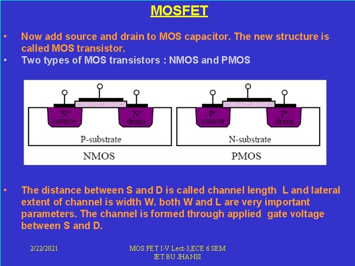
• • • MOSFET Now add source and drain to MOS capacitor. The new structure is called MOS transistor. Two types of MOS transistors : NMOS and PMOS The distance between S and D is called channel length L and lateral extent of channel is width W. both W and L are very important parameters. The channel is formed through applied gate voltage between S and D. 2/22/2021 MOS FET I-V Lect-3, ECE 6 SEM IET BU JHANSI

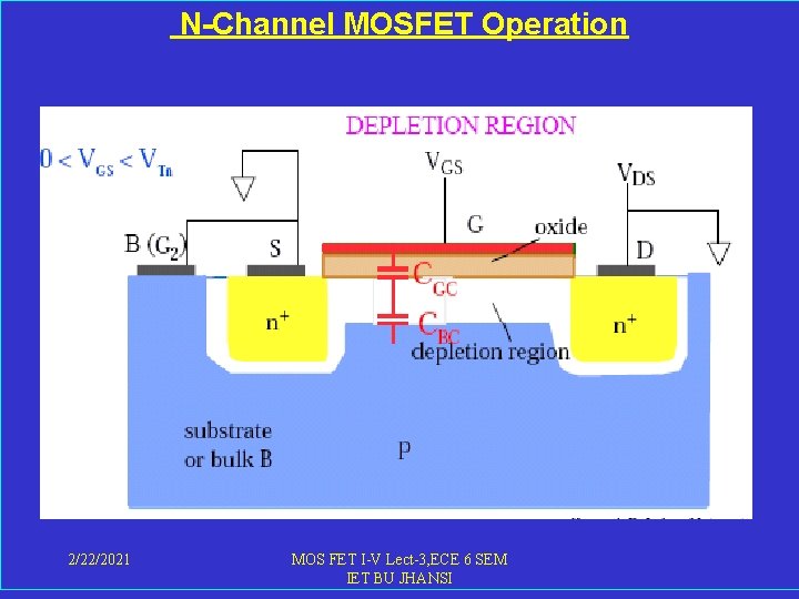
N-Channel MOSFET Operation 2/22/2021 MOS FET I-V Lect-3, ECE 6 SEM IET BU JHANSI

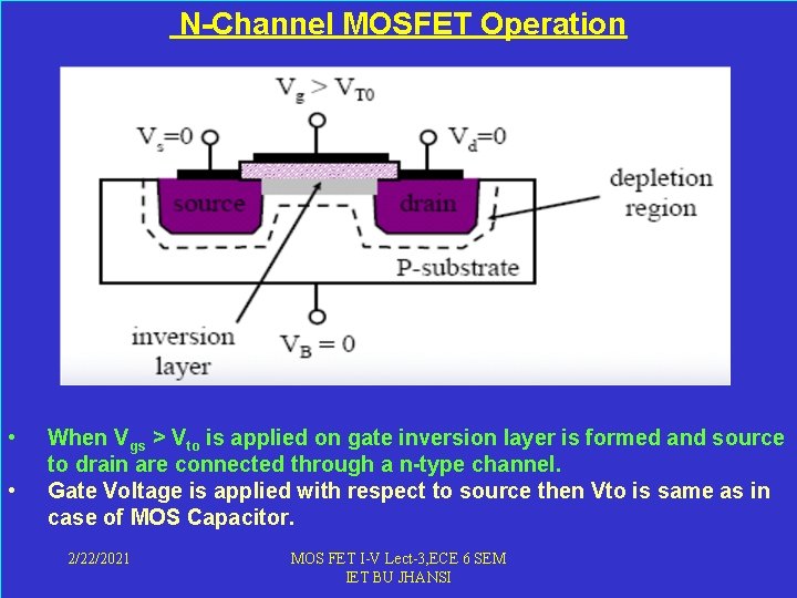
N-Channel MOSFET Operation • • When Vgs > Vto is applied on gate inversion layer is formed and source to drain are connected through a n-type channel. Gate Voltage is applied with respect to source then Vto is same as in case of MOS Capacitor. 2/22/2021 MOS FET I-V Lect-3, ECE 6 SEM IET BU JHANSI

2/22/2021 MOS FET I-V Lect-3, ECE 6 SEM IET BU JHANSI

2/22/2021 MOS FET I-V Lect-3, ECE 6 SEM IET BU JHANSI

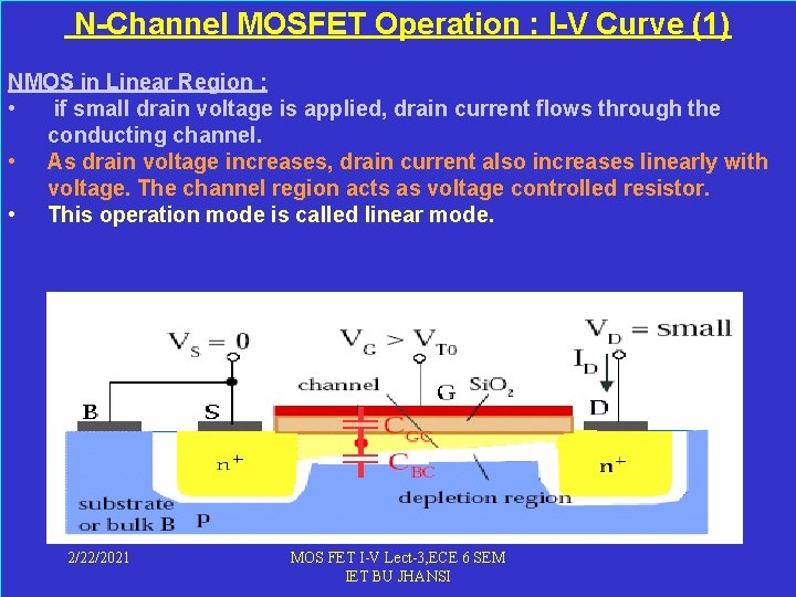
N-Channel MOSFET Operation : I-V Curve (1) NMOS in Linear Region : • if small drain voltage is applied, drain current flows through the conducting channel. • As drain voltage increases, drain current also increases linearly with voltage. The channel region acts as voltage controlled resistor. • This operation mode is called linear mode. 2/22/2021 MOS FET I-V Lect-3, ECE 6 SEM IET BU JHANSI

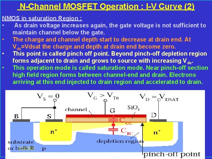
N-Channel MOSFET Operation : I-V Curve (2) NMOS in saturation Region : • As drain voltage increases again, the gate voltage is not sufficient to maintain channel below the gate. • The charge and channel depth start to decrease at drain end. At Vds=Vdsat the charge and depth at drain end become zero. • This point is called pinch off point. Beyond pinch-off depletion region forms adjacent to drain and grows to source with increasing V ds. • This operation mode is called saturation mode. Near pinch-off section high field region forms between channel-end and drain. Electrons arriving at this end injected to drain region and accelerated to drain. 2/22/2021 MOS FET I-V Lect-3, ECE 6 SEM IET BU JHANSI

N-Channel MOSFET Operation : I-V Curve (3) • 3 -D analysis of this system is very complex to establish the I-V relation of NMOS. • Several approximations be made to simplify the problem. • The Gradual-Channel Approximation (GCA) is used which converts 3 D problem into 1 -D for analytic derivation of I-V. 2/22/2021 MOS FET I-V Lect-3, ECE 6 SEM IET BU JHANSI

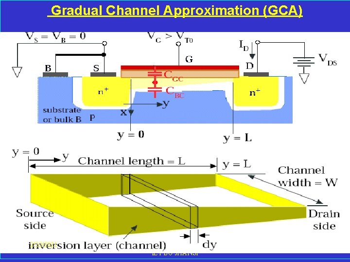
Gradual Channel Approximation (GCA) 2/22/2021 MOS FET I-V Lect-3, ECE 6 SEM IET BU JHANSI

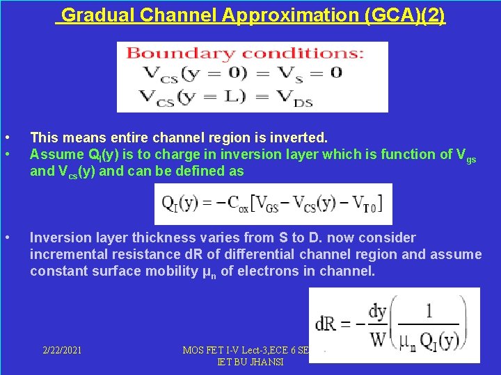
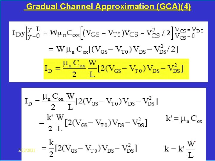
Gradual Channel Approximation (GCA)(2) • • This means entire channel region is inverted. Assume QI(y) is to charge in inversion layer which is function of V gs and Vcs(y) and can be defined as • Inversion layer thickness varies from S to D. now consider incremental resistance d. R of differential channel region and assume constant surface mobility μn of electrons in channel. 2/22/2021 MOS FET I-V Lect-3, ECE 6 SEM IET BU JHANSI

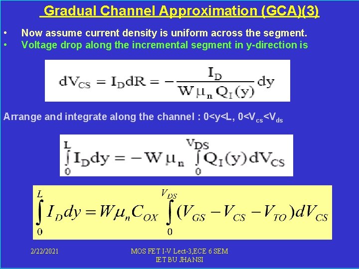
Gradual Channel Approximation (GCA)(3) • • Now assume current density is uniform across the segment. Voltage drop along the incremental segment in y-direction is Arrange and integrate along the channel : 0<y<L, 0<Vcs<Vds 2/22/2021 MOS FET I-V Lect-3, ECE 6 SEM IET BU JHANSI

Gradual Channel Approximation (GCA)(4) 2/22/2021 MOS FET I-V Lect-3, ECE 6 SEM IET BU JHANSI

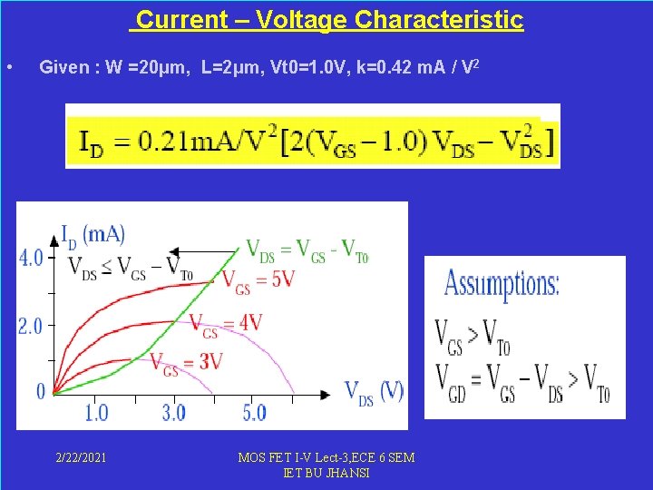
Current – Voltage Characteristic • Given : W =20μm, L=2μm, Vt 0=1. 0 V, k=0. 42 m. A / V 2 2/22/2021 MOS FET I-V Lect-3, ECE 6 SEM IET BU JHANSI

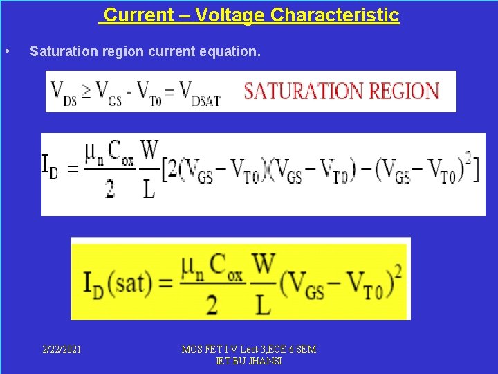
Current – Voltage Characteristic • Saturation region current equation. 2/22/2021 MOS FET I-V Lect-3, ECE 6 SEM IET BU JHANSI

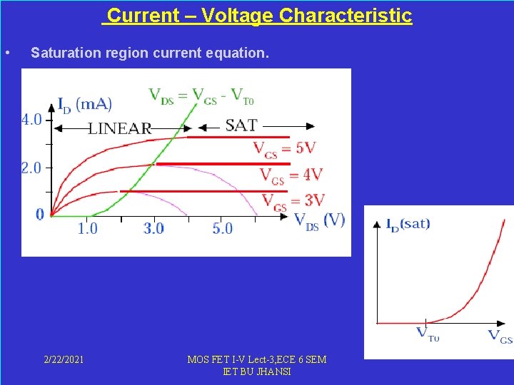
Current – Voltage Characteristic • Saturation region current equation. 2/22/2021 MOS FET I-V Lect-3, ECE 6 SEM IET BU JHANSI

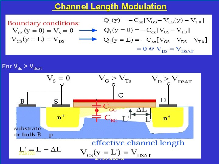
Channel Length Modulation For Vds > Vdsat 2/22/2021 MOS FET I-V Lect-3, ECE 6 SEM IET BU JHANSI

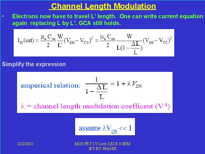
Channel Length Modulation • Electrons now have to travel L’ length. One can write current equation again replacing L by L’. GCA still holds. Simplify the expression 2/22/2021 MOS FET I-V Lect-3, ECE 6 SEM IET BU JHANSI

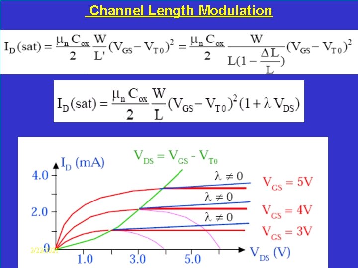
Channel Length Modulation 2/22/2021 MOS FET I-V Lect-3, ECE 6 SEM IET BU JHANSI

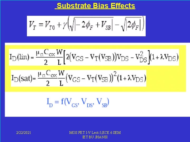
Substrate Bias Effects 2/22/2021 MOS FET I-V Lect-3, ECE 6 SEM IET BU JHANSI

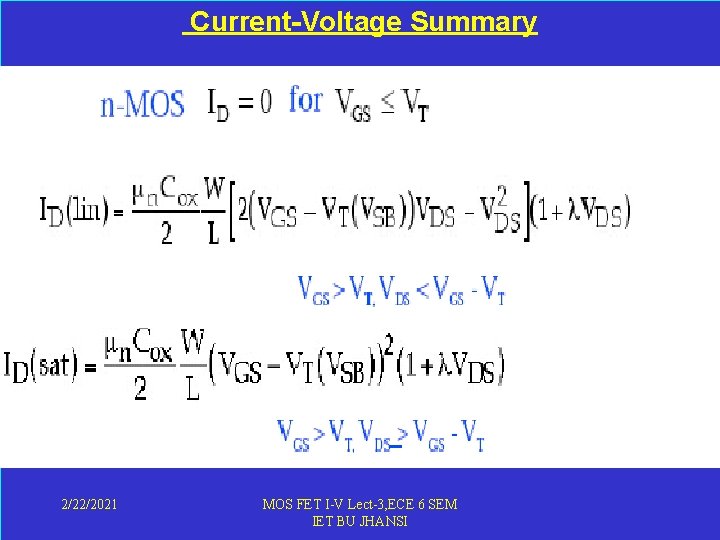
Current-Voltage Summary 2/22/2021 MOS FET I-V Lect-3, ECE 6 SEM IET BU JHANSI

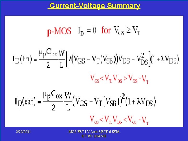
Current-Voltage Summary 2/22/2021 MOS FET I-V Lect-3, ECE 6 SEM IET BU JHANSI

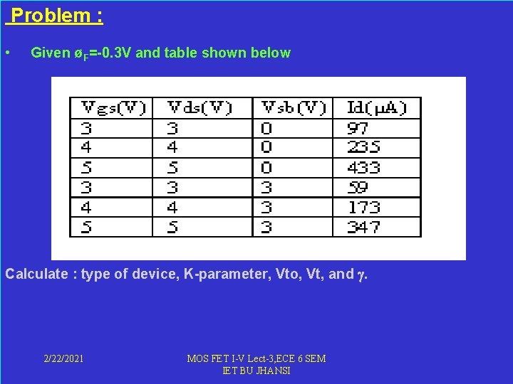
Problem : • Given øF=-0. 3 V and table shown below Calculate : type of device, K-parameter, Vto, Vt, and . 2/22/2021 MOS FET I-V Lect-3, ECE 6 SEM IET BU JHANSI

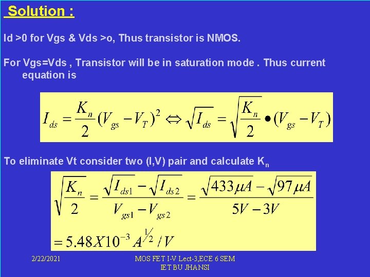
Solution : Id >0 for Vgs & Vds >o, Thus transistor is NMOS. For Vgs=Vds , Transistor will be in saturation mode. Thus current equation is To eliminate Vt consider two (I, V) pair and calculate Kn 2/22/2021 MOS FET I-V Lect-3, ECE 6 SEM IET BU JHANSI

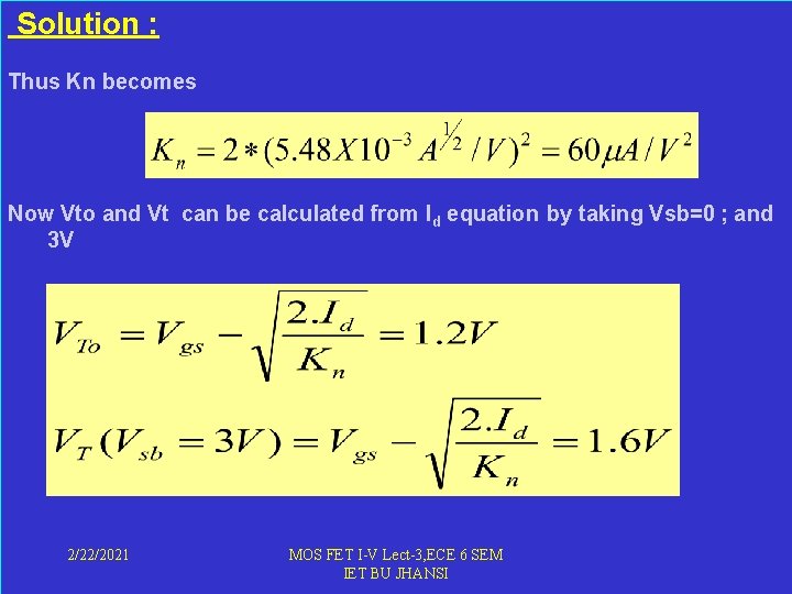
Solution : Thus Kn becomes Now Vto and Vt can be calculated from Id equation by taking Vsb=0 ; and 3 V 2/22/2021 MOS FET I-V Lect-3, ECE 6 SEM IET BU JHANSI

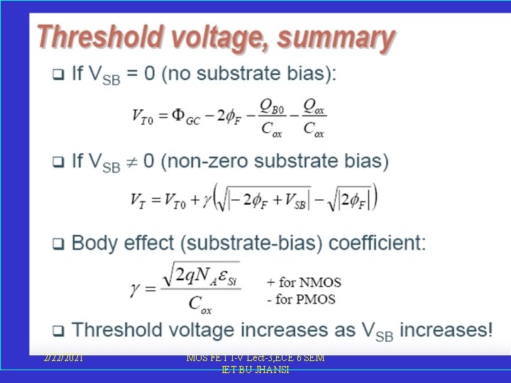
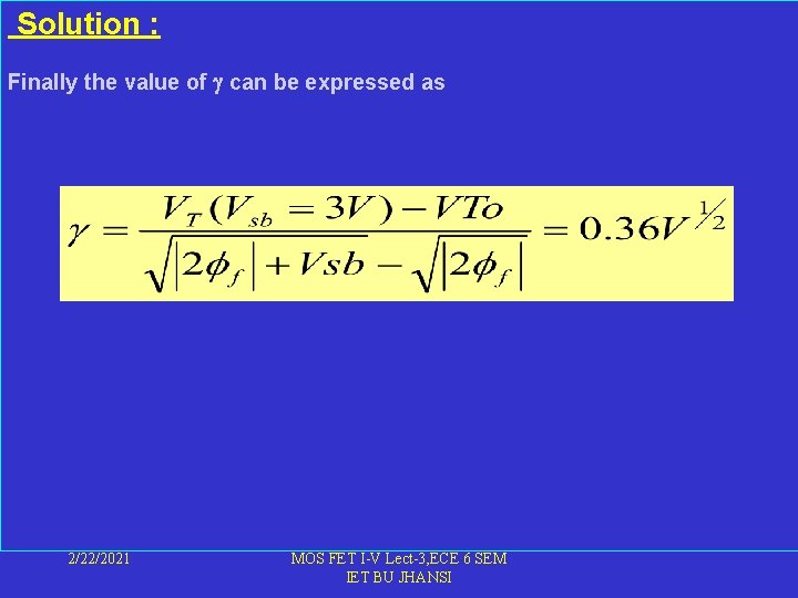
Solution : Finally the value of can be expressed as 2/22/2021 MOS FET I-V Lect-3, ECE 6 SEM IET BU JHANSI

Next Class Topic Depletion Type MOSFET Scaling and Small Geometry Effects. 2/22/2021 MOS FET I-V Lect-3, ECE 6 SEM IET BU JHANSI