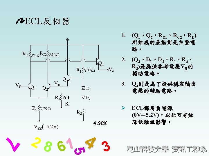
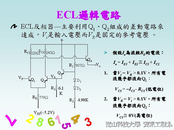
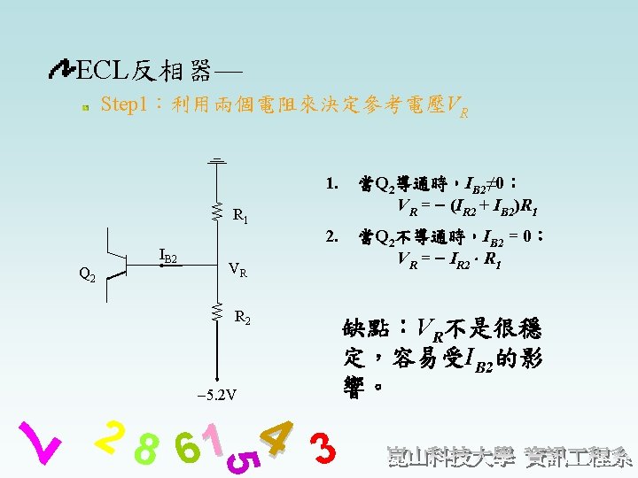
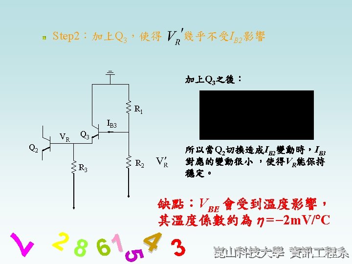
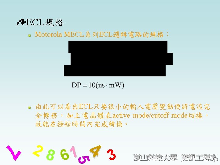
CMOS Nchannel MOSFET Pchannel MOSFET Complementary MOSCMOS VDD


。 VDD Qp Vi Vo Qn 7")


且Vtn = |Vtp| = Vt 。 Vo")


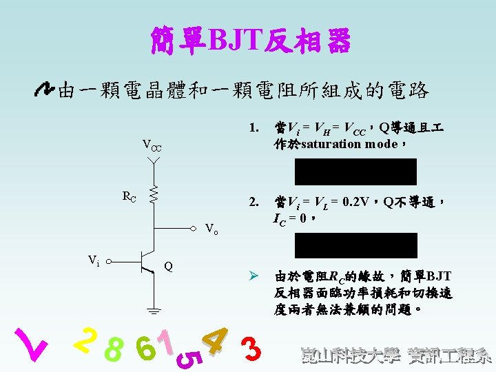
 當Vi = VCC時: 必須適當選擇RB和RC,才能使BJT 作在 saturation mode。所以: 7 4 3 5")


- Slides: 63
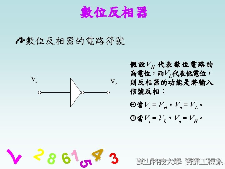
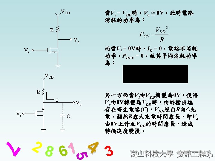
天才設計-CMOS反相器 由N-channel MOSFET及 P-channel MOSFET 組合而成,兩者具有互補作用,故稱為 Complementary MOS(CMOS)。 VDD Qp Vi Vo Qn 7 4 3 5 28 1 6 用一顆P-channel MOSFET取代簡 單反相器中的R
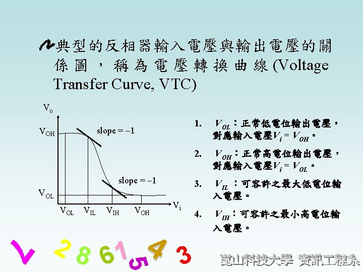
CMOS反相器特性 電壓轉換曲線 Ø 假設使用enhancement-type的 MOSFET,Vtn及Vtp 分別表示 Qn及Qp的臨界電壓(Vtn為正值, Vtp為負值)且Vtn = |Vtp| = Vt 。 Vo VOH = VDD slope = 1 Ø Qn:VGS = Vi VDS = Vo VGS, eff = Vi Vt slope = 1 VOL = 0 VIL VIH VDD 7 4 3 5 28 1 6 Ø QP: VSG = VDD Vi VSD = VDD Vo Vi VSG, eff = VDD Vi Vt
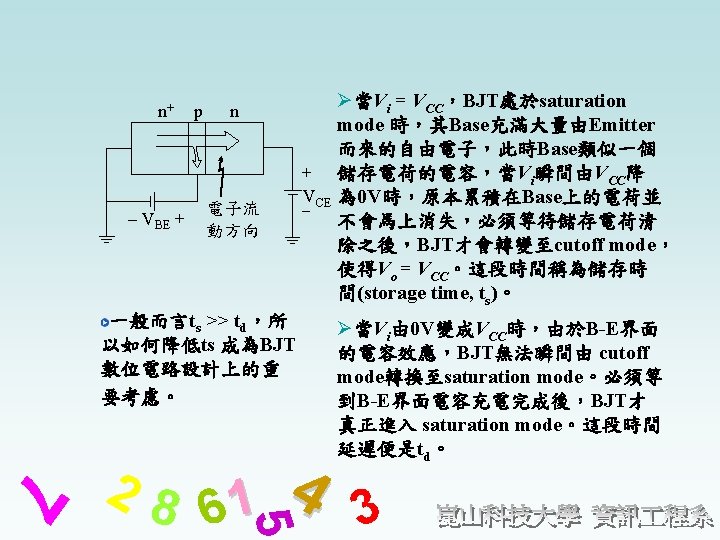
BJT轉換特性 數位電路的應用上主要將BJT 作在cutoff 及saturation兩個mode VCC RC Vo Vi Q 7 4 3 5 28 1 6 由於PN-junction內部的 電容效應,使得BJT無 法瞬間由cutoff mode轉 換至saturation mode, 反之亦然。
Resistor-Transistor Logic (RTL) 當Vi = VCC時: 必須適當選擇RB和RC,才能使BJT 作在 saturation mode。所以: 7 4 3 5 28 1 6
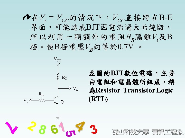
TTL邏輯電路 TTL inverter的標準電路 VCC = 5 V R 3 4 K R 4 130 R 2 1. 6 K Q 2 Vi Q 3 Q 4 VBE(ON) = 0. 7 V VCE(sat) = 0. 2 V D Vo Q 1 R 1 1 K 7 4 3 5 28 1 6 Ø 當Vi = VH,各個電晶體的 作模式為: Q 4:inverse active mode Q 3:saturation mode Q 1:saturation mode Q 2:cutoff mode D:OFF Ø 當Vi = VL(假定VL = 0. 2 V), 各電晶體 作模式為: Q 4:saturation mode Q 3:cutoff mode Q 1:cutoff mode Q 2:active mode D:ON
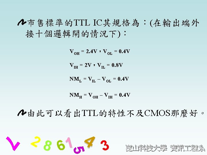
TTL特性 電壓轉換曲線 在輸出端不接任何邏輯 閘的情況下: Vo 3. 7 V VOH 3. 7 V,VOL 0. 1 V 2. 7 V VIH 1. 4 V,VIL 0. 5 V 0. 1 V 0. 5 1. 2 1. 4 7 Vi(V) 4 3 5 28 1 6 NML = VIL – VOL = 0. 4 V NMH = VOH – VIH = 2. 3 V