CMOS Layout Design Dr Zakir Ali Asstt Prof

- Slides: 26
CMOS Layout Design Dr. Zakir Ali, Asstt. Prof. Deptt. OF ECE. Email : zakirali 008@gmail. com 2/25/2021 Layout-design Lect-8,
FABRICATION OF MOSFET 2/25/2021 Layout-design Lect-8,
Introduction IC technologies : • • • NMOS PMOS CMOS SOI Bi. CMOS Ga. As 2/25/2021 Layout-design Lect-8,
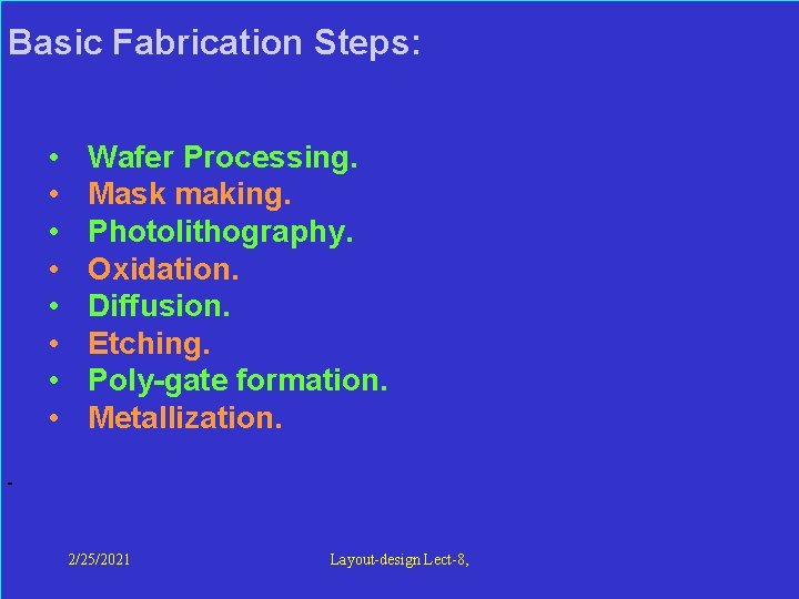
Basic Fabrication Steps: • • Wafer Processing. Mask making. Photolithography. Oxidation. Diffusion. Etching. Poly-gate formation. Metallization. 2/25/2021 Layout-design Lect-8,
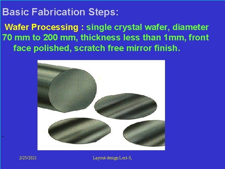
Basic Fabrication Steps: Wafer Processing : single crystal wafer, diameter 70 mm to 200 mm, thickness less than 1 mm, front face polished, scratch free mirror finish. 2/25/2021 Layout-design Lect-8,
Basic Fabrication Steps: Mask making : • After complete design the drawing is broken into subsequent IC processing steps. • These steps are called mask levels. • Electron beam machine known as pattern generator is used for mask making. • The interface is CIF between layout and mask machine. • Mask machine transfers design features directly on photosensitive glass plate using CIF. 2/25/2021 Layout-design Lect-8,
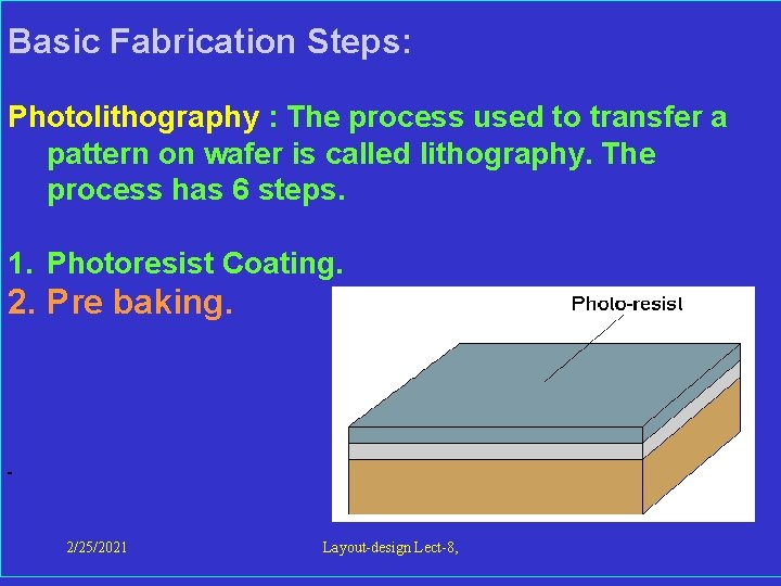
Basic Fabrication Steps: Photolithography : The process used to transfer a pattern on wafer is called lithography. The process has 6 steps. 1. Photoresist Coating. 2. Pre baking. 2/25/2021 Layout-design Lect-8,
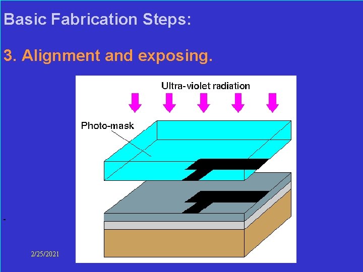
Basic Fabrication Steps: 3. Alignment and exposing. 2/25/2021 Layout-design Lect-8,
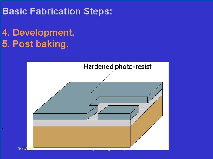
Basic Fabrication Steps: 4. Development. 5. Post baking. 2/25/2021 Layout-design Lect-8,
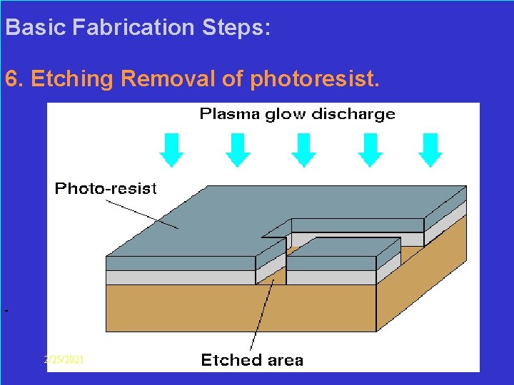
Basic Fabrication Steps: 6. Etching Removal of photoresist. 2/25/2021 Layout-design Lect-8,
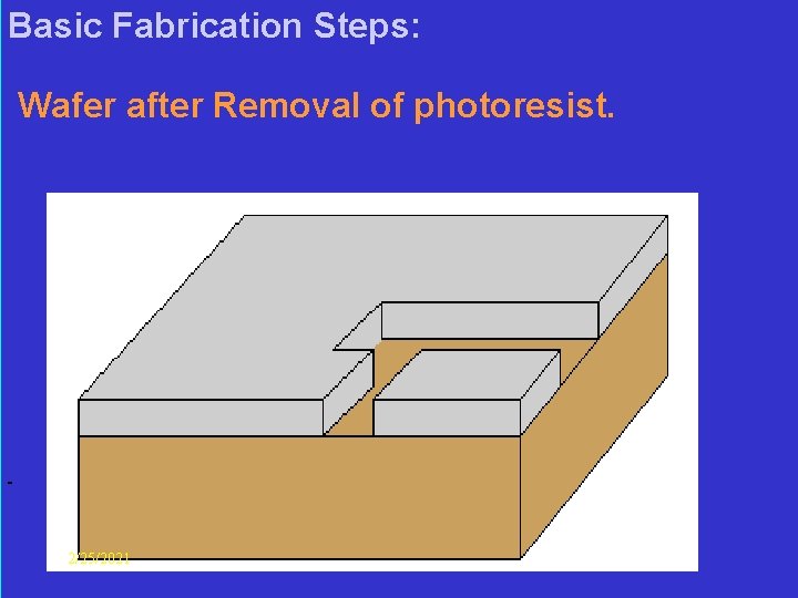
Basic Fabrication Steps: Wafer after Removal of photoresist. 2/25/2021 Layout-design Lect-8,
Basic Fabrication Steps: Oxidation : The purpose of Si. O 2 layer is 1. acts as component in MOS. 2. acts as mask against diffusion. 3. used to isolate the devices 4. provides electrical isolation in multilevel metallization. Several techniques : thermal oxidation, wet oxidation, CVD, Plasma oxidation. LOCOS Oxidation for isolation. 2/25/2021 Layout-design Lect-8,
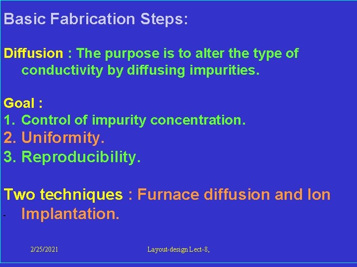
Basic Fabrication Steps: Diffusion : The purpose is to alter the type of conductivity by diffusing impurities. Goal : 1. Control of impurity concentration. 2. Uniformity. 3. Reproducibility. Two techniques : Furnace diffusion and Ion Implantation. 2/25/2021 Layout-design Lect-8,
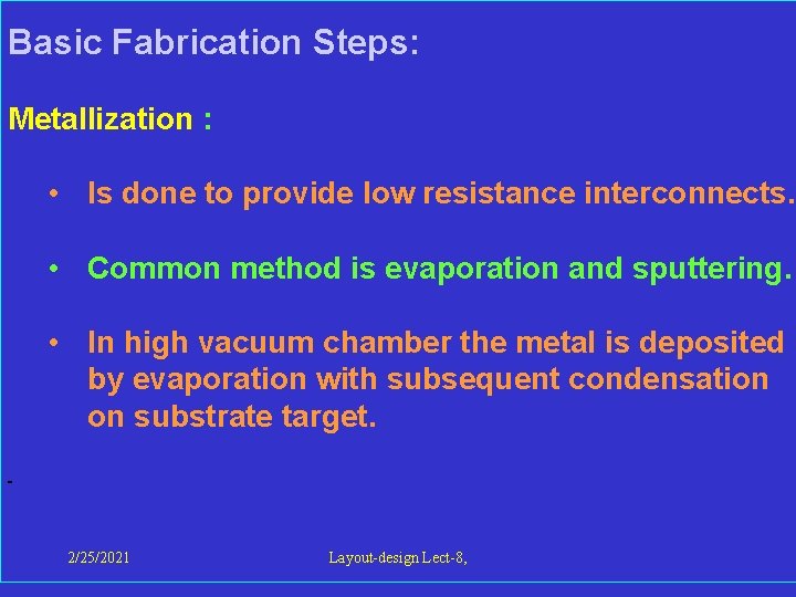
Basic Fabrication Steps: Metallization : • Is done to provide low resistance interconnects. • Common method is evaporation and sputtering. • In high vacuum chamber the metal is deposited by evaporation with subsequent condensation on substrate target. 2/25/2021 Layout-design Lect-8,
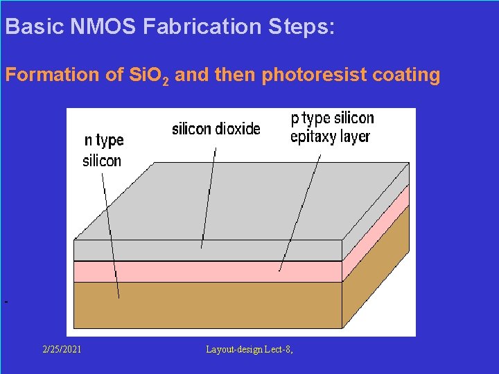
Basic NMOS Fabrication Steps: Formation of Si. O 2 and then photoresist coating 2/25/2021 Layout-design Lect-8,
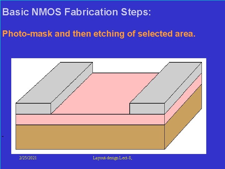
Basic NMOS Fabrication Steps: Photo-mask and then etching of selected area. 2/25/2021 Layout-design Lect-8,
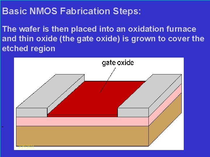
Basic NMOS Fabrication Steps: The wafer is then placed into an oxidation furnace and thin oxide (the gate oxide) is grown to cover the etched region 2/25/2021 Layout-design Lect-8,
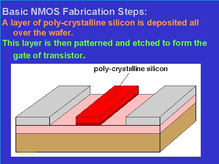
Basic NMOS Fabrication Steps: A layer of poly-crystalline silicon is deposited all over the wafer. This layer is then patterned and etched to form the gate of transistor. 2/25/2021 Layout-design Lect-8,
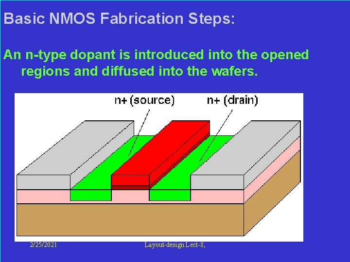
Basic NMOS Fabrication Steps: An n-type dopant is introduced into the opened regions and diffused into the wafers. 2/25/2021 Layout-design Lect-8,
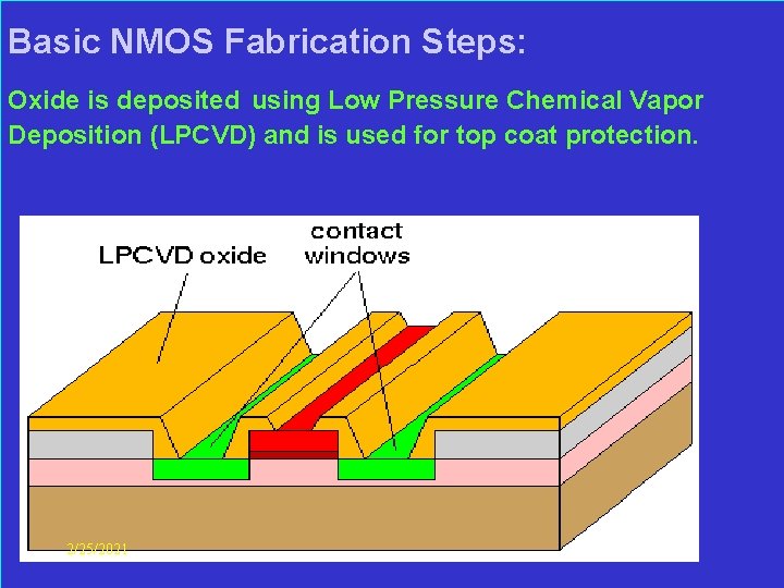
Basic NMOS Fabrication Steps: Oxide is deposited using Low Pressure Chemical Vapor Deposition (LPCVD) and is used for top coat protection. 2/25/2021 Layout-design Lect-8,
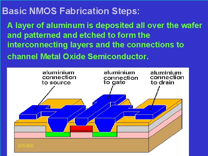
Basic NMOS Fabrication Steps: A layer of aluminum is deposited all over the wafer and patterned and etched to form the interconnecting layers and the connections to channel Metal Oxide Semiconductor. 2/25/2021 Layout-design Lect-8,
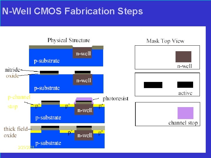
N-Well CMOS Fabrication Steps 2/25/2021 Layout-design Lect-8,
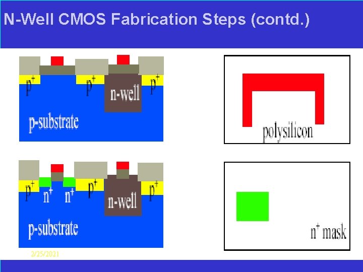
N-Well CMOS Fabrication Steps (contd. ) 2/25/2021 Layout-design Lect-8,
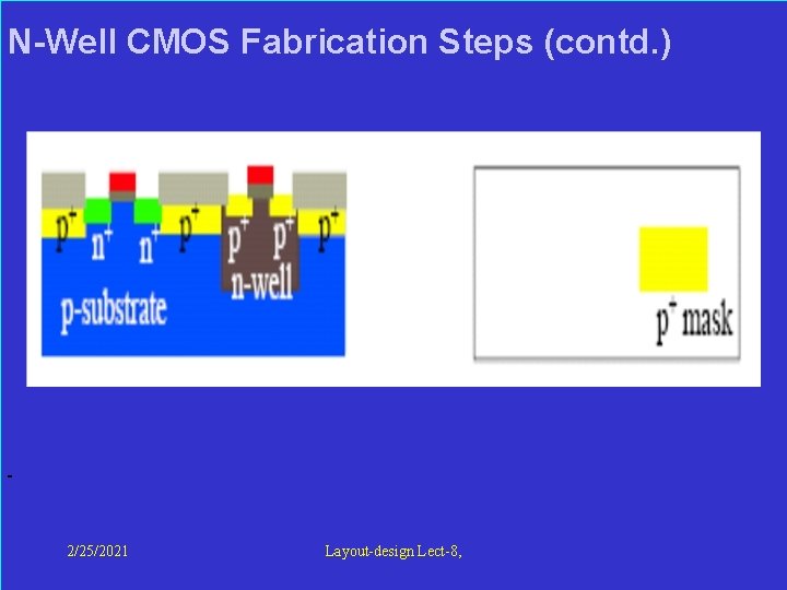
N-Well CMOS Fabrication Steps (contd. ) 2/25/2021 Layout-design Lect-8,
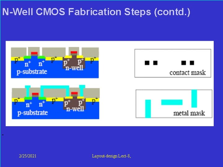
N-Well CMOS Fabrication Steps (contd. ) 2/25/2021 Layout-design Lect-8,
Next Class Topic Design Rules and MOS Transistor 2/25/2021 Layout-design Lect-8,