CHAPTER 6 MOSFET RELATED DEVICES Part 2 MOSFET

- Slides: 18

CHAPTER 6: MOSFET & RELATED DEVICES Part 2

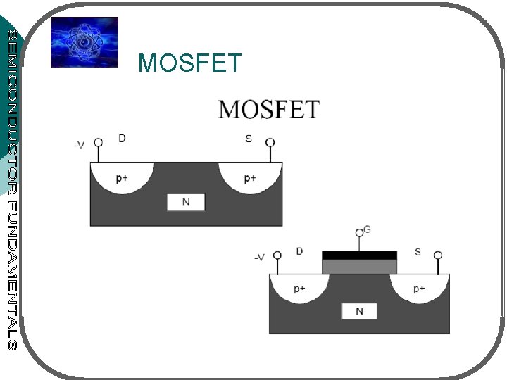
MOSFET

MOSFET

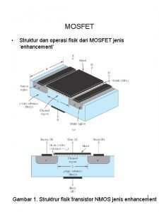
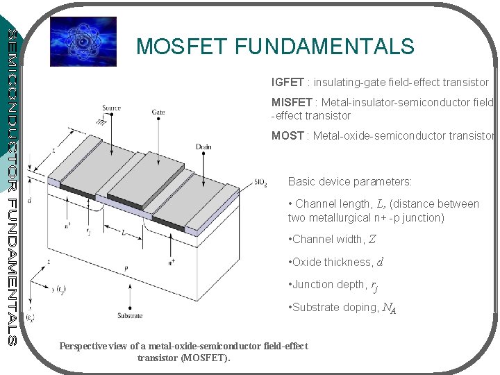
MOSFET FUNDAMENTALS IGFET : insulating-gate field-effect transistor MISFET : Metal-insulator-semiconductor field -effect transistor MOST : Metal-oxide-semiconductor transistor Basic device parameters: • Channel length, L, (distance between two metallurgical n+ -p junction) • Channel width, Z • Oxide thickness, d • Junction depth, rj • Substrate doping, NA Perspective view of a metal-oxide-semiconductor field-effect transistor (MOSFET).

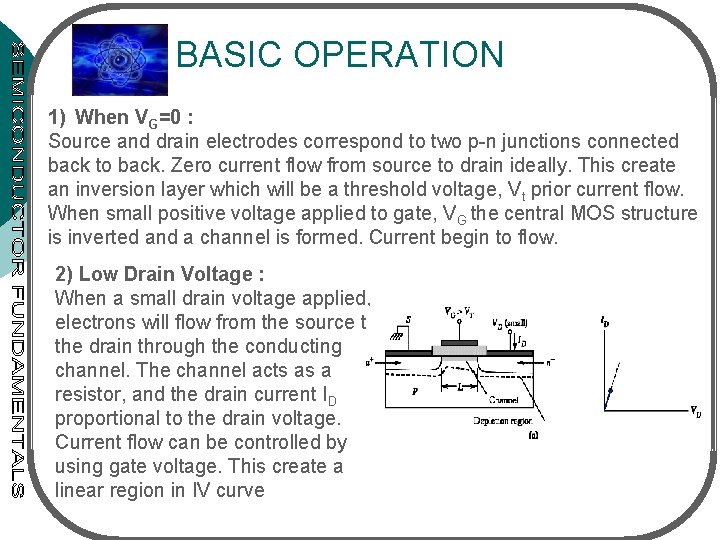
BASIC OPERATION 1) When VG=0 : Source and drain electrodes correspond to two p-n junctions connected back to back. Zero current flow from source to drain ideally. This create an inversion layer which will be a threshold voltage, Vt prior current flow. When small positive voltage applied to gate, VG the central MOS structure is inverted and a channel is formed. Current begin to flow. 2) Low Drain Voltage : When a small drain voltage applied, electrons will flow from the source to the drain through the conducting channel. The channel acts as a resistor, and the drain current ID proportional to the drain voltage. Current flow can be controlled by using gate voltage. This create a linear region in IV curve

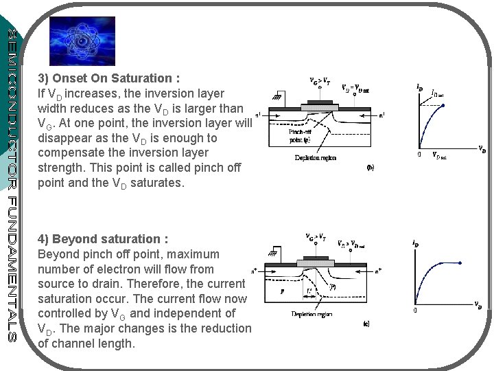
3) Onset On Saturation : If VD increases, the inversion layer width reduces as the VD is larger than VG. At one point, the inversion layer will disappear as the VD is enough to compensate the inversion layer strength. This point is called pinch off point and the VD saturates. 4) Beyond saturation : Beyond pinch off point, maximum number of electron will flow from source to drain. Therefore, the current saturation occur. The current flow now controlled by VG and independent of VD. The major changes is the reduction of channel length.

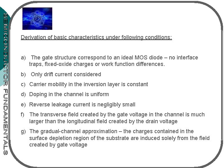
Derivation of basic characteristics under following conditions: a) The gate structure correspond to an ideal MOS diode – no interface traps, fixed-oxide charges or work function differences. b) Only drift current considered c) Carrier mobility in the inversion layer is constant d) Doping in the channel is uniform e) Reverse leakage current is negligibly small f) The transverse field created by the gate voltage in the channel is much larger than the longitudinal field created by the drain voltage g) The gradual-channel approximation – the charges contained in the surface depletion region of the substrate are induced solely from the field created by gate voltage

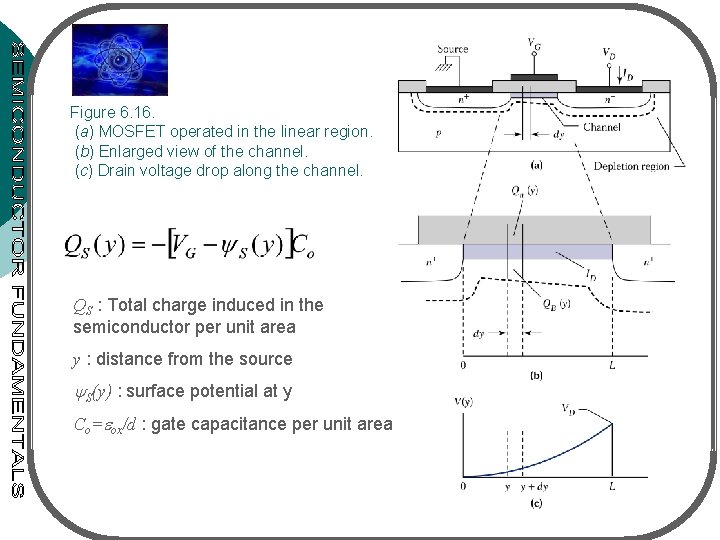
Figure 6. 16. (a) MOSFET operated in the linear region. (b) Enlarged view of the channel. (c) Drain voltage drop along the channel. QS : Total charge induced in the semiconductor per unit area y : distance from the source S(y) : surface potential at y Co= ox/d : gate capacitance per unit area

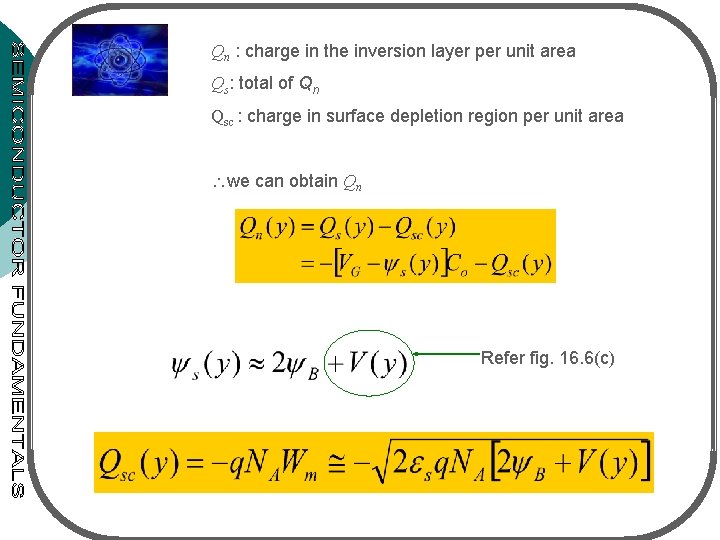
Qn : charge in the inversion layer per unit area Qs: total of Qn Qsc : charge in surface depletion region per unit area we can obtain Qn Refer fig. 16. 6(c)

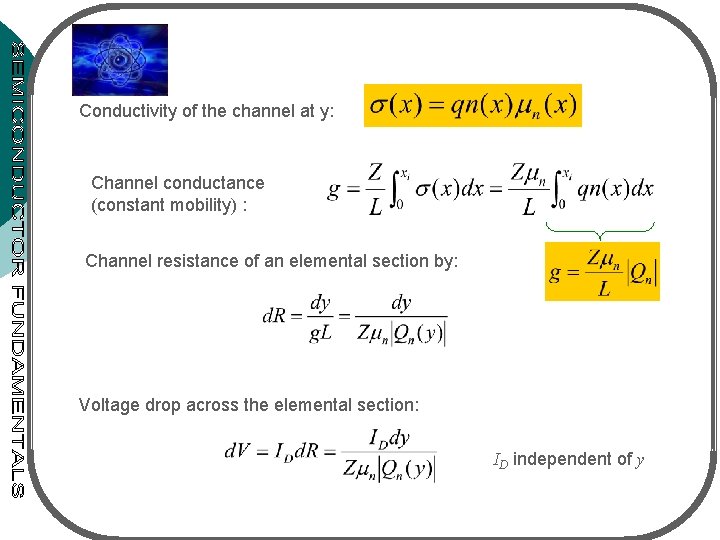
Conductivity of the channel at y: Channel conductance (constant mobility) : Channel resistance of an elemental section by: Voltage drop across the elemental section: ID independent of y

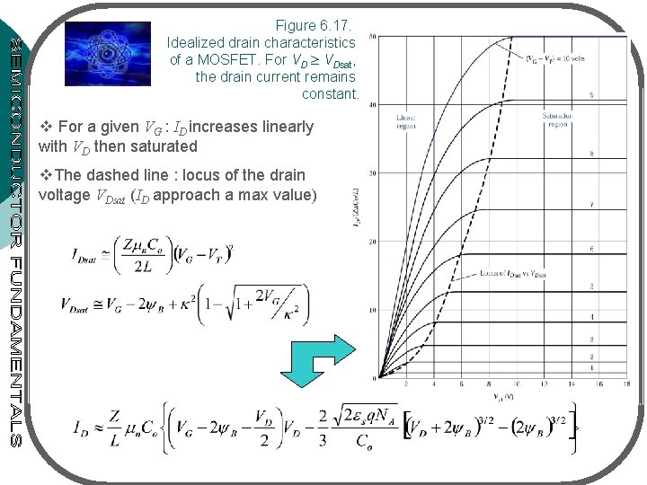
Figure 6. 17. Idealized drain characteristics of a MOSFET. For VD VDsat, the drain current remains constant. v For a given VG : ID increases linearly with VD then saturated v. The dashed line : locus of the drain voltage VDsat (ID approach a max value)

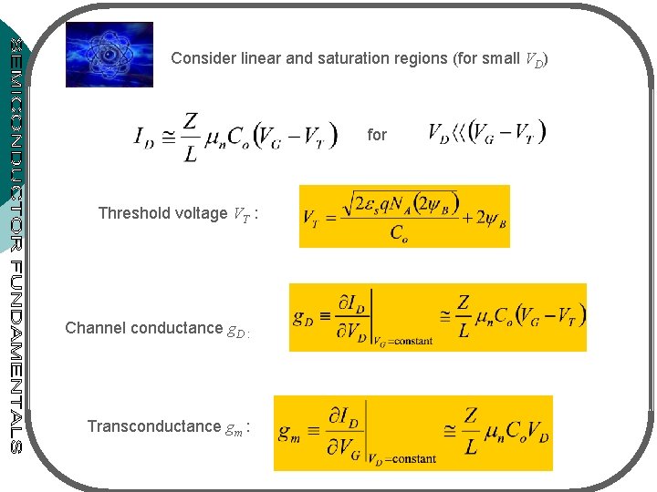
Consider linear and saturation regions (for small VD) for Threshold voltage VT : Channel conductance g. D : Transconductance gm :

v Pinch-off point : VD increased to a point that charge Qn(y) in the inversion layer at y=L number of mobile ē at the drain are reduced drastically v At this point VD & ID VDsat & IDsat v VD > VDsat saturation region

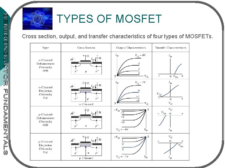
TYPES OF MOSFET Cross section, output, and transfer characteristics of four types of MOSFETs.

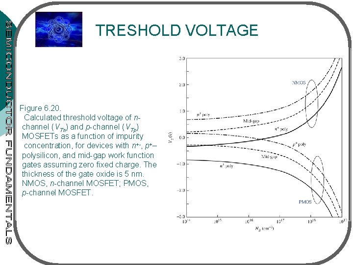
TRESHOLD VOLTAGE Figure 6. 20. Calculated threshold voltage of nchannel (VTn) and p-channel (VTp) MOSFETs as a function of impurity concentration, for devices with n+-, p+– polysilicon, and mid-gap work function gates assuming zero fixed charge. The thickness of the gate oxide is 5 nm. NMOS, n-channel MOSFET; PMOS, p-channel MOSFET.

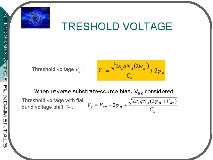
TRESHOLD VOLTAGE Threshold voltage VT : When reverse substrate-source bias, VBS considered Threshold voltage with flat band voltage shift VT :

MOSFET APPLICATION ¡ MOSFET applied in the semiconductor industry for : a) VLSI Circuits b) Memory Devices ( DRAM, SRAM, Nonvolatile Memory) c) CMOS Digital Circuit d) Microprocessors ¡ Advantages of MOSFET : a) In CMOS, perfect zero current when input switch off. Good logic ‘ 1’ and logic ‘ 0’ condition. b) Ability to scale down in size. (Channel length, width, area) c) Ability to control threshold voltage when device shrink. Quick switching. d) Oxide layer between gate and channel prevent DC flow – Power Consumption. e) Low power consumption allow more components per chip surface area.

DISADVANTAGES OF MOSFET ¡ ¡ ¡ Reduces VT makes MOSFET could not switched off – weak inversion layer. Interconnect capacitance between wires – device miniature reduces. Heat production impact – shrink device size, increasing device quantity. Thin oxide requirement – gate oxide tunneling leakage problem. Increased process fabrication steps – complex circuit design.
 Two types of physical fitness
 Benefits of skill related fitness
 All literary devices
 Input or output devices of computer
 Literary devices in fahrenheit 451 part 3
 What is bureaucratic control dystopia
 Lsb and msb in binary
 Addition symbol
 Unit ratio definition
 Part part whole
 Part by part technical description example
 What are the 3 parts of the bar
 The phase of the moon you see depends on ______.
 Minitab adalah
 Chapter 5 skill related fitness crossword
 Makenzie milton injury
 Chapter 16 worksheet the knee and related structures
 Income statement kieso
 Fet transistori


