Lecture 22 OUTLINE The MOSFET contd MOSFET scaling
- Slides: 21

Lecture 22 OUTLINE The MOSFET (cont’d) • MOSFET scaling • Velocity saturation • Short channel effects Reading: Pierret 19. 1; Hu 7. 1, 7. 3

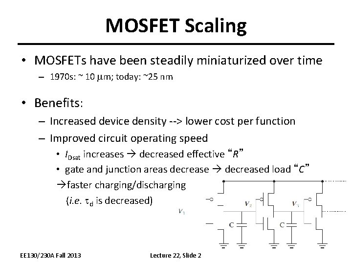
MOSFET Scaling • MOSFETs have been steadily miniaturized over time – 1970 s: ~ 10 mm; today: ~25 nm • Benefits: – Increased device density --> lower cost per function – Improved circuit operating speed • IDsat increases decreased effective “R” • gate and junction areas decreased load “C” faster charging/discharging (i. e. td is decreased) EE 130/230 A Fall 2013 Lecture 22, Slide 2

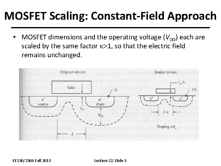
MOSFET Scaling: Constant-Field Approach • MOSFET dimensions and the operating voltage (VDD) each are scaled by the same factor k>1, so that the electric field remains unchanged. EE 130/230 A Fall 2013 Lecture 22, Slide 3

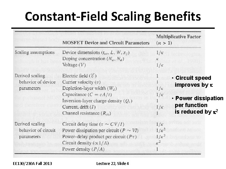
Constant-Field Scaling Benefits • Circuit speed improves by k • Power dissipation per function is reduced by k 2 EE 130/230 A Fall 2013 Lecture 22, Slide 4

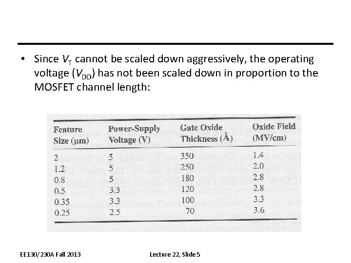
• Since VT cannot be scaled down aggressively, the operating voltage (VDD) has not been scaled down in proportion to the MOSFET channel length: EE 130/230 A Fall 2013 Lecture 22, Slide 5

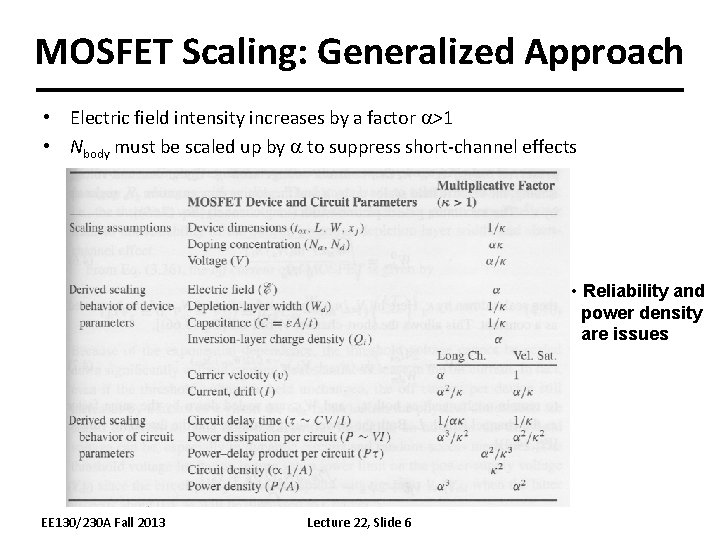
MOSFET Scaling: Generalized Approach • Electric field intensity increases by a factor a>1 • Nbody must be scaled up by a to suppress short-channel effects • Reliability and power density are issues EE 130/230 A Fall 2013 Lecture 22, Slide 6

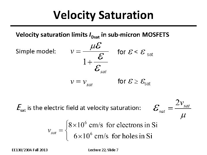
Velocity Saturation Velocity saturation limits IDsat in sub-micron MOSFETS Simple model: for e < e sat for e esat Esat is the electric field at velocity saturation: EE 130/230 A Fall 2013 Lecture 22, Slide 7

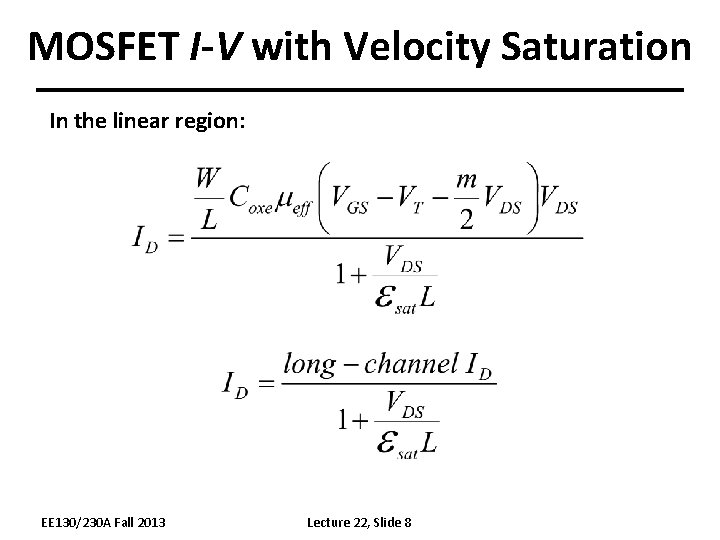
MOSFET I-V with Velocity Saturation In the linear region: EE 130/230 A Fall 2013 Lecture 22, Slide 8

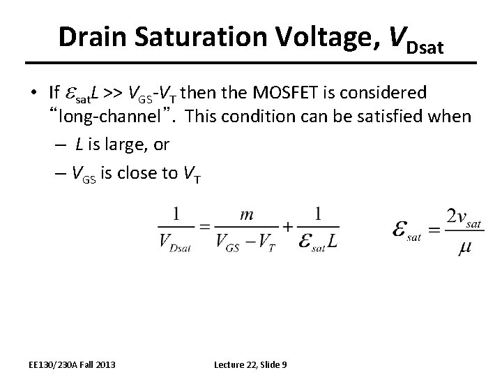
Drain Saturation Voltage, VDsat • If esat. L >> VGS-VT then the MOSFET is considered “long-channel”. This condition can be satisfied when – L is large, or – VGS is close to VT EE 130/230 A Fall 2013 Lecture 22, Slide 9

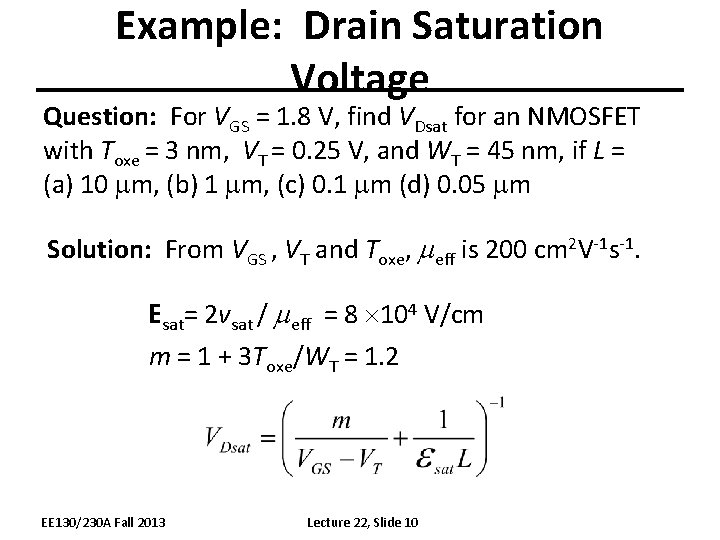
Example: Drain Saturation Voltage Question: For VGS = 1. 8 V, find VDsat for an NMOSFET with Toxe = 3 nm, VT = 0. 25 V, and WT = 45 nm, if L = (a) 10 mm, (b) 1 mm, (c) 0. 1 mm (d) 0. 05 mm Solution: From VGS , VT and Toxe, meff is 200 cm 2 V-1 s-1. Esat= 2 vsat / meff = 8 104 V/cm m = 1 + 3 Toxe/WT = 1. 2 EE 130/230 A Fall 2013 Lecture 22, Slide 10

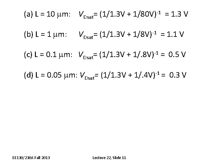
(a) L = 10 mm: VDsat= (1/1. 3 V + 1/80 V)-1 = 1. 3 V (b) L = 1 mm: VDsat= (1/1. 3 V + 1/8 V)-1 = 1. 1 V (c) L = 0. 1 mm: VDsat= (1/1. 3 V + 1/. 8 V)-1 = 0. 5 V (d) L = 0. 05 mm: VDsat= (1/1. 3 V + 1/. 4 V)-1 = 0. 3 V EE 130/230 A Fall 2013 Lecture 22, Slide 11

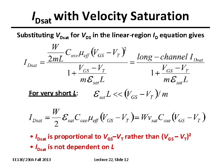
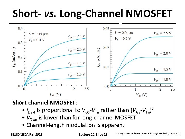
IDsat with Velocity Saturation Substituting VDsat for VDS in the linear-region ID equation gives For very short L: • IDsat is proportional to VGS–VT rather than (VGS – VT)2 • IDsat is not dependent on L EE 130/230 A Fall 2013 Lecture 22, Slide 12

Short- vs. Long-Channel NMOSFET Short-channel NMOSFET: • IDsat is proportional to VGS-VTn rather than (VGS-VTn)2 • VDsat is lower than for long-channel MOSFET • Channel-length modulation is apparent EE 130/230 A Fall 2013 Lecture 22, Slide 13 C. C. Hu, Modern Semiconductor Devices for Integrated Circuits, Figure 6 -23

Velocity Overshoot • When L is comparable to or less than the mean free path, some of the electrons travel through the channel without experiencing a single scattering event projectile-like motion (“ballistic transport”) Þ The average velocity of carriers exceeds vsat e. g. 35% for L = 0. 12 mm NMOSFET Þ Effectively, vsat and esat increase when L is very small EE 130/230 A Fall 2013 Lecture 22, Slide 14

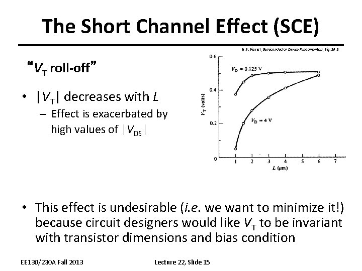
The Short Channel Effect (SCE) R. F. Pierret, Semiconductor Device Fundamentals, Fig. 19. 3 “VT roll-off” • |VT| decreases with L – Effect is exacerbated by high values of |VDS| • This effect is undesirable (i. e. we want to minimize it!) because circuit designers would like VT to be invariant with transistor dimensions and bias condition EE 130/230 A Fall 2013 Lecture 22, Slide 15

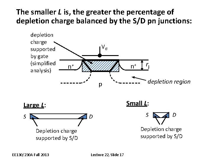
Qualitative Explanation of SCE • Before an inversion layer forms beneath the gate, the surface of the Si underneath the gate must be depleted (to a depth WT) • The source & drain pn junctions assist in depleting the Si underneath the gate – Portions of the depletion charge in the channel region are balanced by charge in S/D regions, rather than by charge on the gate Þ Less gate charge is required to invert the semiconductor surface (i. e. |VT| decreases) EE 130/230 A Fall 2013 Lecture 22, Slide 16

The smaller L is, the greater the percentage of depletion charge balanced by the S/D pn junctions: depletion charge supported by gate (simplified analysis) VG n+ n+ p D S D Depletion charge supported by S/D EE 130/230 A Fall 2013 depletion region Small L: Large L: S rj Lecture 22, Slide 17

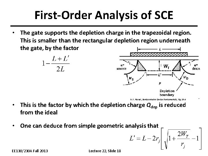
First-Order Analysis of SCE • The gate supports the depletion charge in the trapezoidal region. This is smaller than the rectangular depletion region underneath the gate, by the factor WT R. F. Pierret, Semiconductor Device Fundamentals, Fig. 19. 4 • This is the factor by which the depletion charge Qdep is reduced from the ideal • One can deduce from simple geometric analysis that EE 130/230 A Fall 2013 Lecture 22, Slide 18

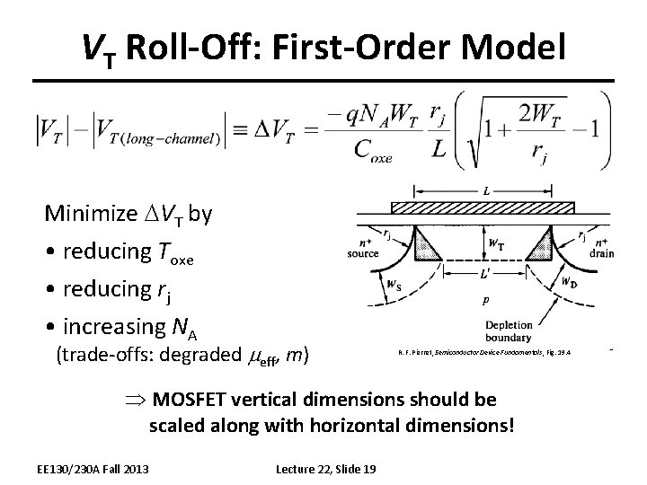
VT Roll-Off: First-Order Model Minimize DVT by • reducing Toxe • reducing rj • increasing NA (trade-offs: degraded meff, m) R. F. Pierret, Semiconductor Device Fundamentals, Fig. 19. 4 Þ MOSFET vertical dimensions should be scaled along with horizontal dimensions! EE 130/230 A Fall 2013 Lecture 22, Slide 19

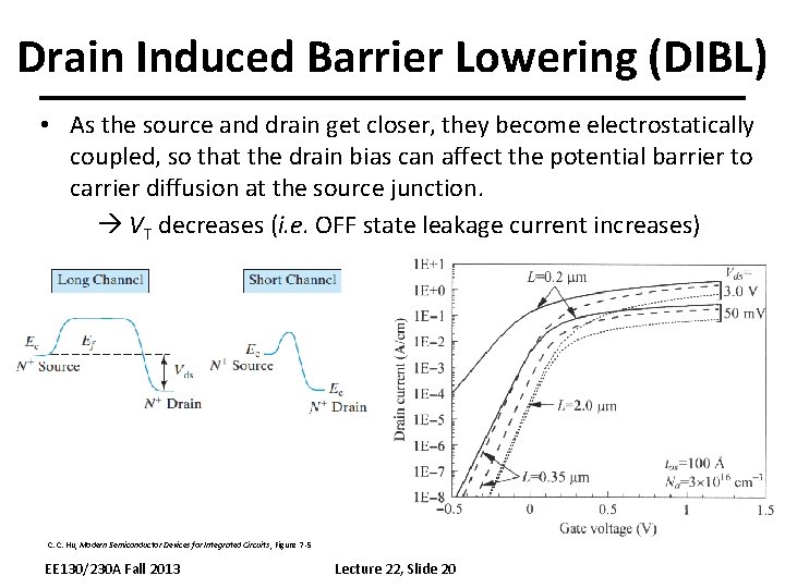
Drain Induced Barrier Lowering (DIBL) • As the source and drain get closer, they become electrostatically coupled, so that the drain bias can affect the potential barrier to carrier diffusion at the source junction. VT decreases (i. e. OFF state leakage current increases) C. C. Hu, Modern Semiconductor Devices for Integrated Circuits, Figure 7 -5 EE 130/230 A Fall 2013 Lecture 22, Slide 20

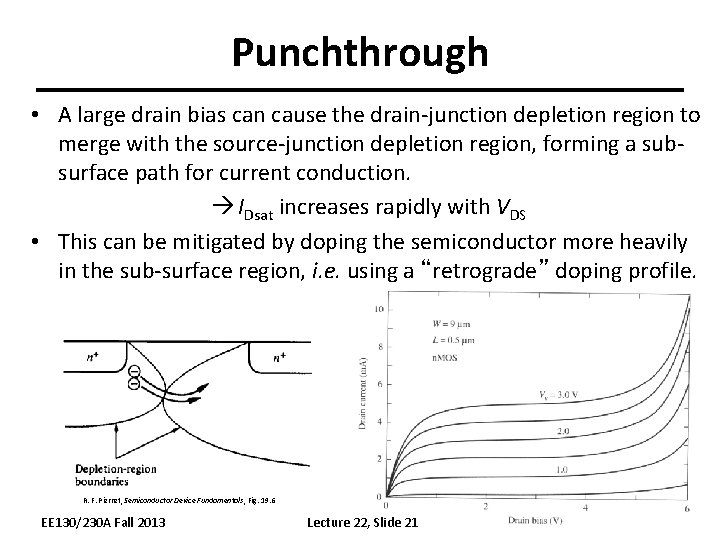
Punchthrough • A large drain bias can cause the drain-junction depletion region to merge with the source-junction depletion region, forming a subsurface path for current conduction. IDsat increases rapidly with VDS • This can be mitigated by doping the semiconductor more heavily in the sub-surface region, i. e. using a “retrograde” doping profile. R. F. Pierret, Semiconductor Device Fundamentals, Fig. 19. 6 EE 130/230 A Fall 2013 Lecture 22, Slide 21