Lecture 23 OUTLINE The MOSFET contd Draininduced effects

- Slides: 13

Lecture 23 OUTLINE The MOSFET (cont’d) • Drain-induced effects • Source/drain structure • CMOS technology Reading: Pierret 19. 1, 19. 2; Hu 6. 10, 7. 3 Optional Reading: Pierret 4; Hu 3

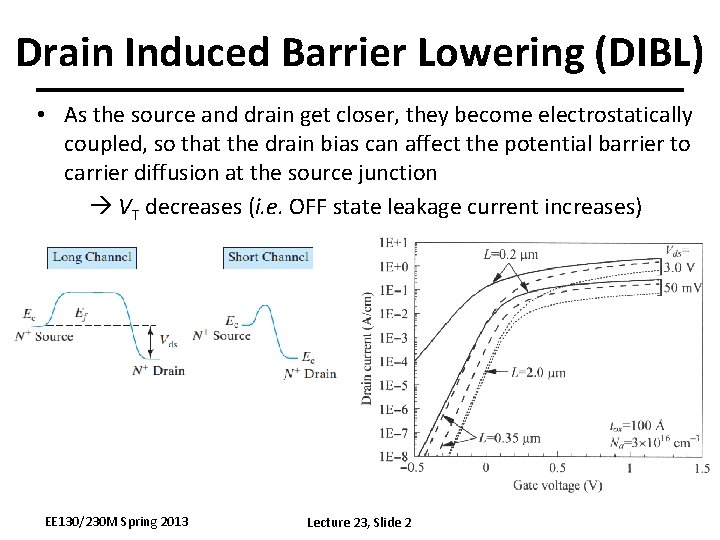
Drain Induced Barrier Lowering (DIBL) • As the source and drain get closer, they become electrostatically coupled, so that the drain bias can affect the potential barrier to carrier diffusion at the source junction VT decreases (i. e. OFF state leakage current increases) EE 130/230 M Spring 2013 Lecture 23, Slide 2

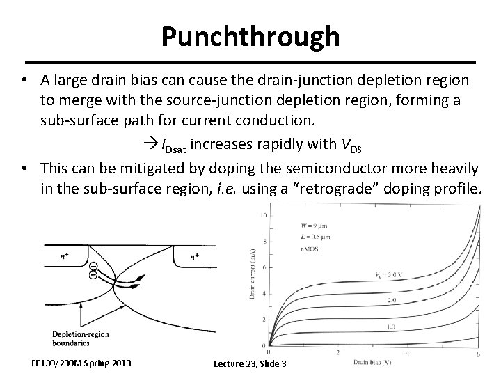
Punchthrough • A large drain bias can cause the drain-junction depletion region to merge with the source-junction depletion region, forming a sub-surface path for current conduction. IDsat increases rapidly with VDS • This can be mitigated by doping the semiconductor more heavily in the sub-surface region, i. e. using a “retrograde” doping profile. EE 130/230 M Spring 2013 Lecture 23, Slide 3

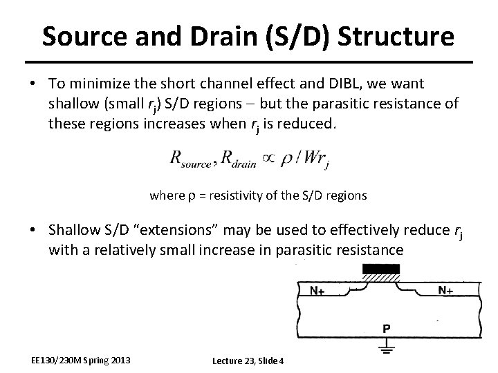
Source and Drain (S/D) Structure • To minimize the short channel effect and DIBL, we want shallow (small rj) S/D regions but the parasitic resistance of these regions increases when rj is reduced. where r = resistivity of the S/D regions • Shallow S/D “extensions” may be used to effectively reduce rj with a relatively small increase in parasitic resistance EE 130/230 M Spring 2013 Lecture 23, Slide 4

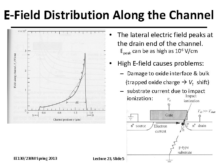
E-Field Distribution Along the Channel • The lateral electric field peaks at the drain end of the channel. Epeak can be as high as 106 V/cm • High E-field causes problems: – Damage to oxide interface & bulk (trapped oxide charge VT shift) – substrate current due to impact ionization: EE 130/230 M Spring 2013 Lecture 23, Slide 5

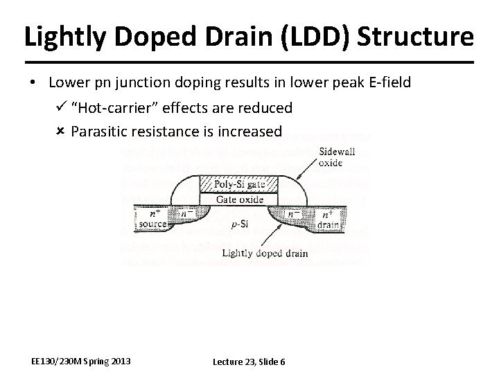
Lightly Doped Drain (LDD) Structure • Lower pn junction doping results in lower peak E-field ü “Hot-carrier” effects are reduced û Parasitic resistance is increased EE 130/230 M Spring 2013 Lecture 23, Slide 6

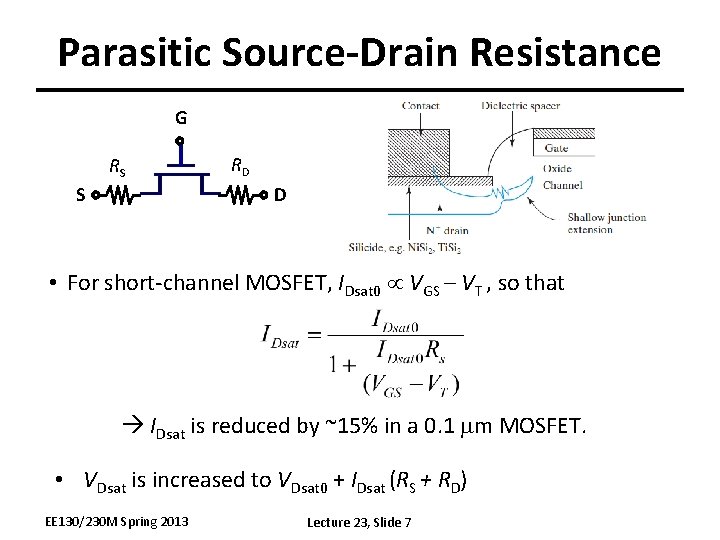
Parasitic Source-Drain Resistance G RS S RD D • For short-channel MOSFET, IDsat 0 VGS – VT , so that IDsat is reduced by ~15% in a 0. 1 mm MOSFET. • VDsat is increased to VDsat 0 + IDsat (RS + RD) EE 130/230 M Spring 2013 Lecture 23, Slide 7

Summary: MOSFET OFF State vs. ON State • OFF state (VGS < VT): – IDS is limited by the rate at which carriers diffuse across the source pn junction – Minimum subthreshold swing S, and DIBL are issues • ON state (VGS > VT): – IDS is limited by the rate at which carriers drift across the channel – Punchthrough is of concern at high drain bias • IDsat increases rapidly with VDS – Parasitic resistances reduce drive current • source resistance RS reduces effective VGS • source & drain resistances RS & RD reduce effective VDS EE 130/230 M Spring 2013 Lecture 23, Slide 8

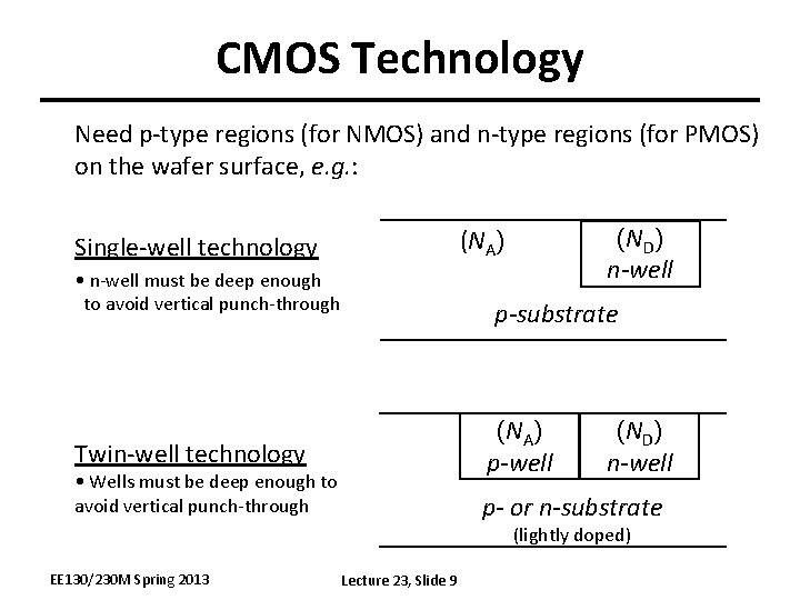
CMOS Technology Need p-type regions (for NMOS) and n-type regions (for PMOS) on the wafer surface, e. g. : (ND) n-well (NA) Single-well technology • n-well must be deep enough to avoid vertical punch-through p-substrate (NA) p-well Twin-well technology • Wells must be deep enough to avoid vertical punch-through (ND) n-well p- or n-substrate (lightly doped) EE 130/230 M Spring 2013 Lecture 23, Slide 9

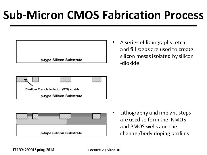
Sub-Micron CMOS Fabrication Process • A series of lithography, etch, and fill steps are used to create silicon mesas isolated by silicon -dioxide • Lithography and implant steps are used to form the NMOS and PMOS wells and the channel/body doping profiles EE 130/230 M Spring 2013 Lecture 23, Slide 10

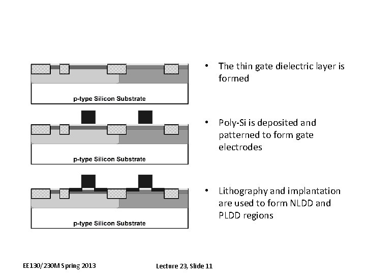
• The thin gate dielectric layer is formed • Poly-Si is deposited and patterned to form gate electrodes • Lithography and implantation are used to form NLDD and PLDD regions EE 130/230 M Spring 2013 Lecture 23, Slide 11

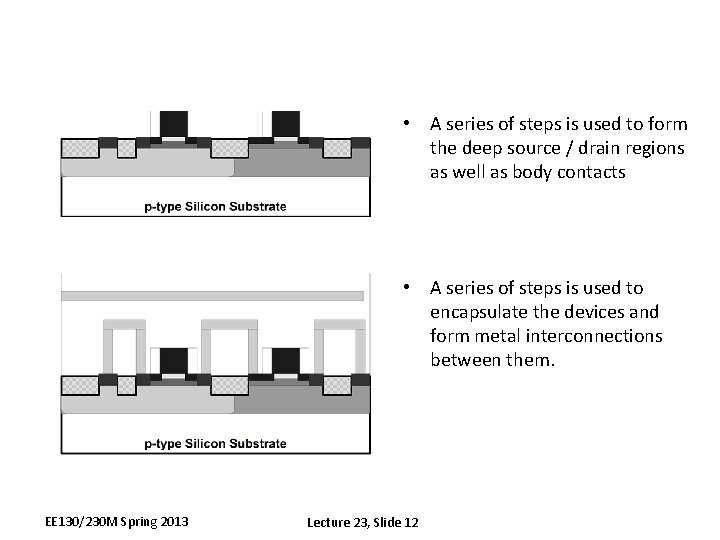
• A series of steps is used to form the deep source / drain regions as well as body contacts • A series of steps is used to encapsulate the devices and form metal interconnections between them. EE 130/230 M Spring 2013 Lecture 23, Slide 12

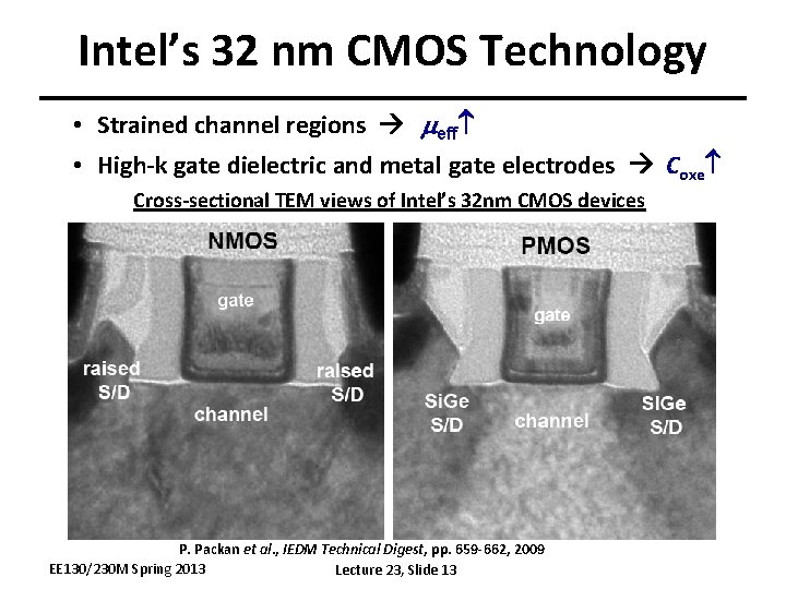
Intel’s 32 nm CMOS Technology • Strained channel regions meff • High-k gate dielectric and metal gate electrodes Coxe Cross-sectional TEM views of Intel’s 32 nm CMOS devices P. Packan et al. , IEDM Technical Digest, pp. 659 -662, 2009 EE 130/230 M Spring 2013 Lecture 23, Slide 13