Lecture 2 The MOSFET The MOSFET as a



- Slides: 40

Lecture 2 The MOSFET

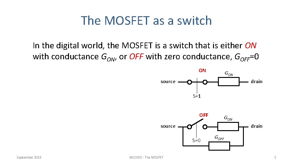
The MOSFET as a switch In the digital world, the MOSFET is a switch that is either ON with conductance GON, or OFF with zero conductance, GOFF=0 gate source ON source GON source drain S=1 drain gate OFF source GON drain source S=0 drain GOFF drain September 2018 MCC 092 - The MOSFET 2

Lecture outline In this lecture we are going to have a closer look at some basic properties of the MOSFET beyond the switch model • Why? • Because, even if the switch model is good enough for designing logic CMOS gates based on their functionality. . . • . . . it is not good enough for determining the performance in terms of switching speed and power dissipation September 2018 MCC 092 - The MOSFET 3

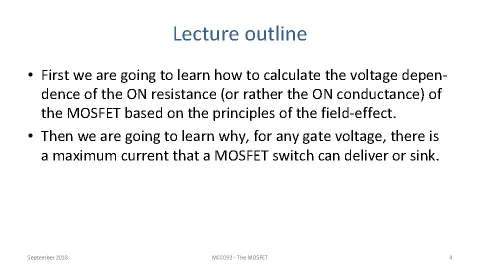
Lecture outline • First we are going to learn how to calculate the voltage dependence of the ON resistance (or rather the ON conductance) of the MOSFET based on the principles of the field-effect. • Then we are going to learn why, for any gate voltage, there is a maximum current that a MOSFET switch can deliver or sink. September 2018 MCC 092 - The MOSFET 4

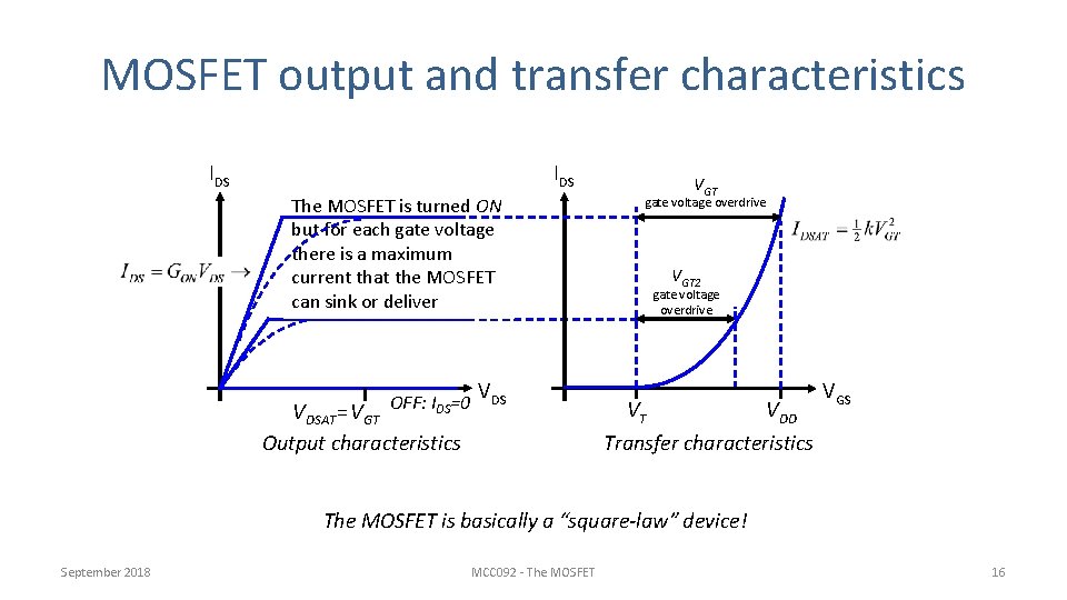
MOSFET output and transfer characteristics IDS The MOSFET is turned ON and for but a current each gate thatvoltage appears to be proportional there is a maximumto VDS starts tothat current flowthe MOSFET can sink or deliver OFF: IDS=0 VDSAT= VGT Output characteristics VDS VGT gate voltage overdrive VGT 2 gate voltage overdrive VT VDD VGS Transfer characteristics The MOSFET is basically a “square-law” device! September 2018 MCC 092 - The MOSFET 5

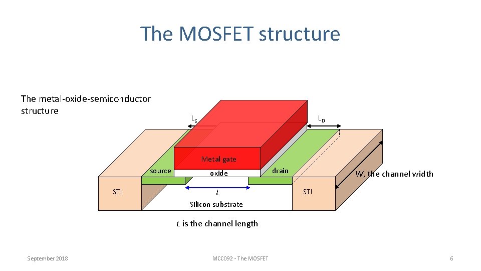
The MOSFET structure The metal-oxide-semiconductor structure LD LS Metal gate source STI oxide L drain W, the channel width STI Silicon substrate L is the channel length September 2018 MCC 092 - The MOSFET 6

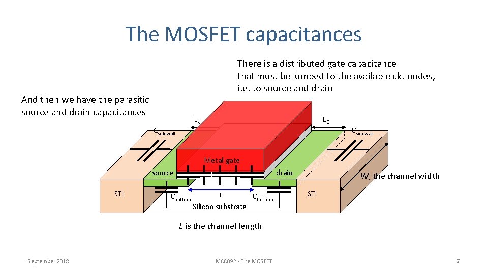
The MOSFET capacitances There is a distributed gate capacitance that must be lumped to the available ckt nodes, i. e. to source and drain And metal-oxide-semiconductor The then we have the parasitic structure source and drain capacitances LD LS Csidewall Metal gate source STI drain Cbottom L Silicon substrate Cbottom W, the channel width STI L is the channel length September 2018 MCC 092 - The MOSFET 7

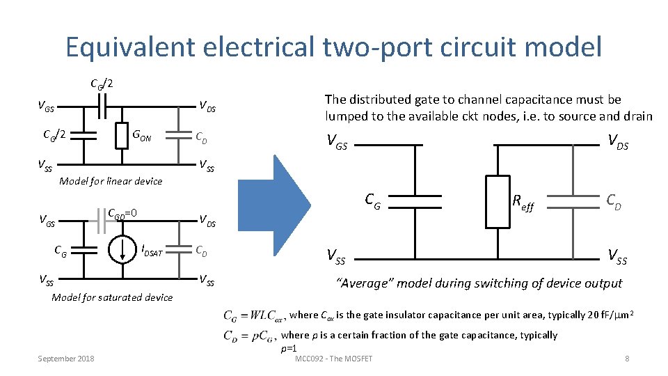
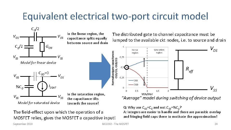
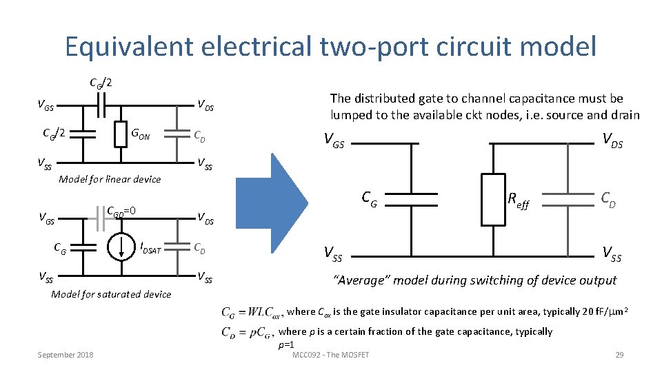
Equivalent electrical two-port circuit model CGD G/2 VGS VDS CGGS/2 VSS GON Model for linear device VGS CG CGD=0 CD The distributed gate to channel capacitance must be lumped to the available ckt nodes, i. e. to source and drain VGS VSS CG VDS IDSAT VSS Model for saturated device VDS CD VSS Reff VSS CD VSS “Average” model during switching of device output where Cox is the gate insulator capacitance per unit area, typically 20 f. F/mm 2 September 2018 where p is a certain fraction of the gate capacitance, typically p=1 MCC 092 - The MOSFET 8

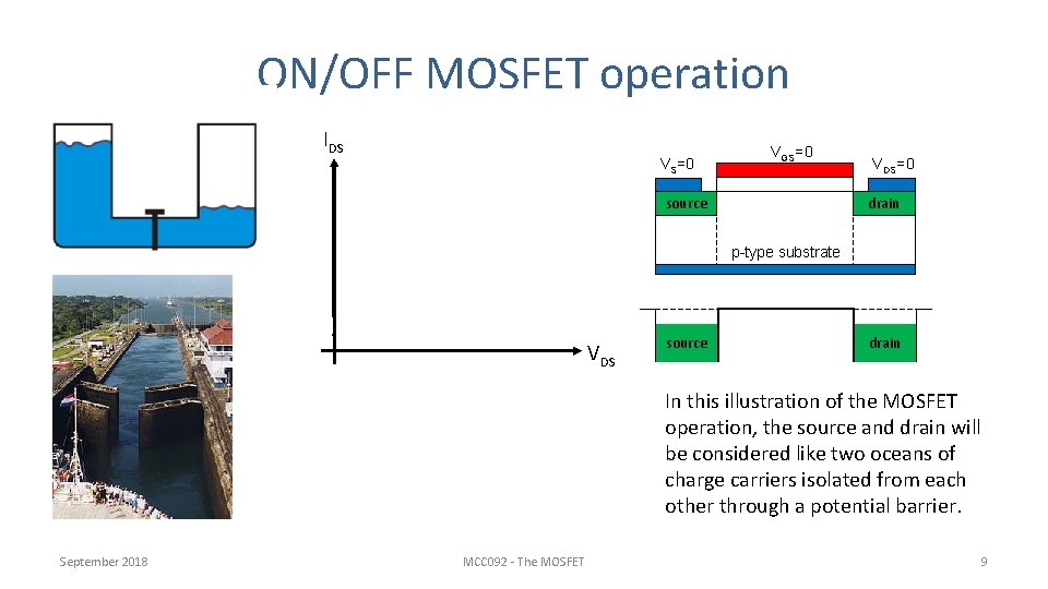
ON/OFF MOSFET operation IDS VS=0 VGS=0 VDS=0 drain source p-type substrate VDS source drain In this illustration of the MOSFET operation, the source and drain will be considered like two oceans of charge carriers isolated from each other through a potential barrier. September 2018 MCC 092 - The MOSFET 9

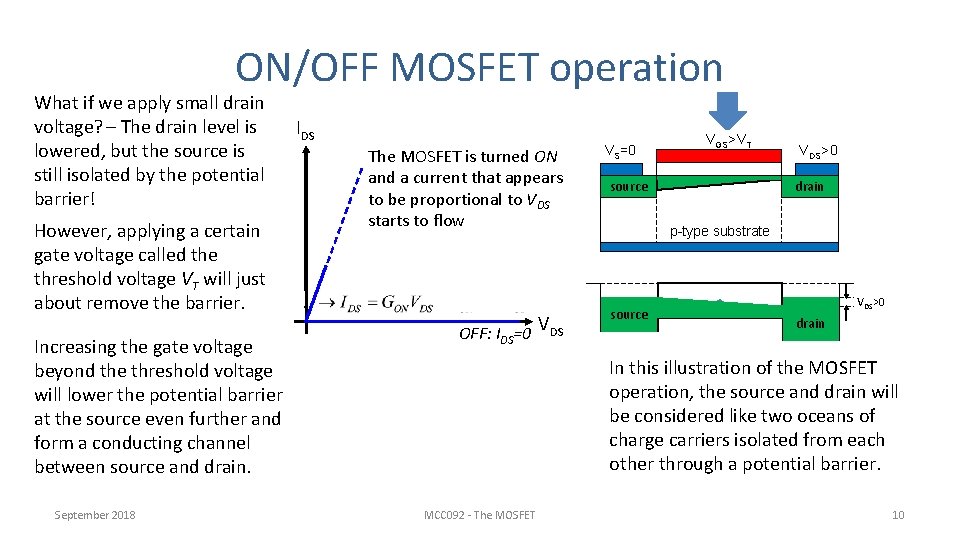
ON/OFF MOSFET operation What if we apply small drain voltage? – The drain level is lowered, but the source is still isolated by the potential barrier! However, applying a certain gate voltage called the threshold voltage VT will just about remove the barrier. Increasing the gate voltage beyond the threshold voltage will lower the potential barrier at the source even further and form a conducting channel between source and drain. September 2018 IDS The MOSFET is turned ON and a current that appears to be proportional to VDS starts to flow OFF: IDS=0 VDS VS=0 VGS>V =0 T =V VDS>0 =0 drain source p-type substrate source drain VDS>0 In this illustration of the MOSFET operation, the source and drain will be considered like two oceans of charge carriers isolated from each other through a potential barrier. MCC 092 - The MOSFET 10

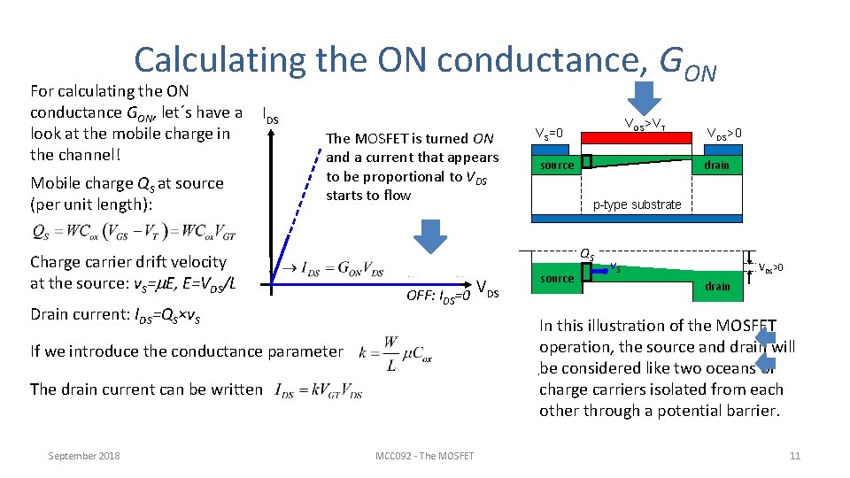
Calculating the ON conductance, GON For calculating the ON conductance GON, let´s have a look at the mobile charge in the channel! IDS Mobile charge QS at source (per unit length): The MOSFET is turned ON and a current that appears to be proportional to VDS starts to flow Charge carrier drift velocity at the source: v. S=m. E, E=VDS/L Drain current: IDS=QS×v. S OFF: IDS=0 VDS>0 drain source p-type substrate QS source v. S VDS>0 drain CIn the gate capacitanceof perthe unit area this illustration MOSFET ox is W is the channel width the source and drain will Voperation, GT =VGS-VT is the gate voltage overdrive 2/Vs] mbe is the charge carrierlike mobility considered two[cmoceans of E=VDS/L is the electric field along the channel If we introduce the conductance parameter charge carriers isolated from each other through a potential barrier. The drain current can be written September 2018 VGS>VT VS=0 MCC 092 - The MOSFET 11

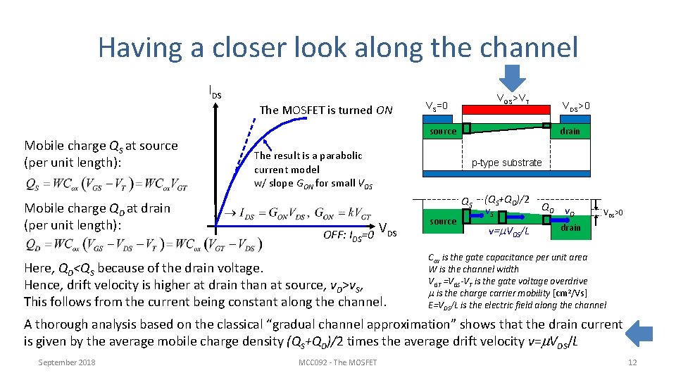
Having a closer look along the channel IDS Mobile charge QS at source (per unit length): Mobile charge QD at drain (per unit length): The MOSFET is turned ON and a current that appears to be proportional to VDS The result a parabolic starts toisflow VGS>VT VS=0 drain source p-type substrate current model w/ slope GON for small VDS QS OFF: IDS=0 VDS Here, QD<QS because of the drain voltage. Hence, drift velocity is higher at drain than at source, v. D>v. S, This follows from the current being constant along the channel. VDS>0 source (QS+QD)/2 v. S v=m. VDS/L QD v D VDS>0 drain Cox is the gate capacitance per unit area W is the channel width VGT =VGS-VT is the gate voltage overdrive m is the charge carrier mobility [cm 2/Vs] E=VDS/L is the electric field along the channel A thorough analysis based on the classical “gradual channel approximation” shows that the drain current is given by the average mobile charge density (QS+QD)/2 times the average drift velocity v=m. VDS/L September 2018 MCC 092 - The MOSFET 12

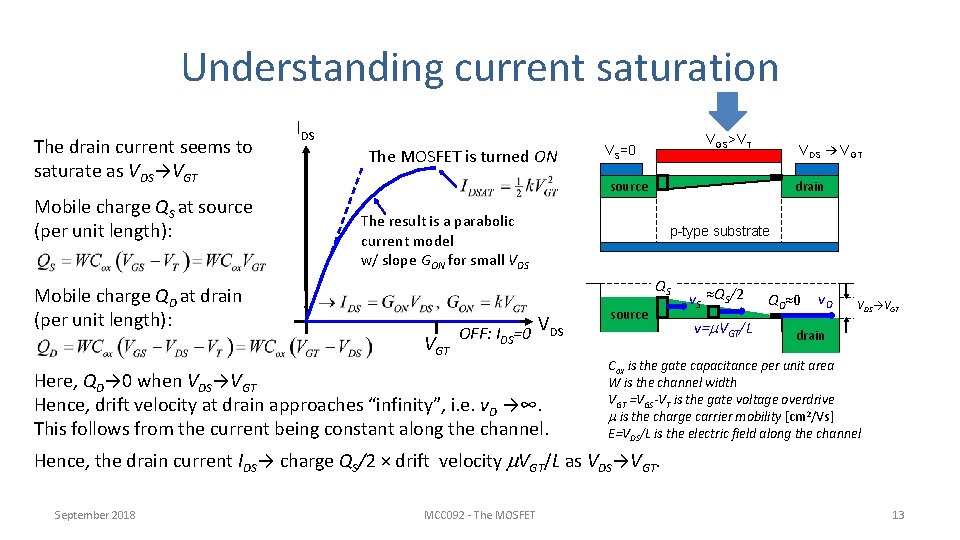
Understanding current saturation The drain current seems to saturate as VDS→VGT Mobile charge QS at source (per unit length): Mobile charge QD at drain (per unit length): IDS The MOSFET is turned ON and a current that appears to be proportional to VDS The result a parabolic starts toisflow VGS>VT VS=0 drain source p-type substrate current model w/ slope GON for small VDS QS VGT OFF: IDS=0 VDS Here, QD→ 0 when VDS→VGT Hence, drift velocity at drain approaches “infinity”, i. e. v. D →∞. This follows from the current being constant along the channel. VDS → VGT source v. S ≈QS/2 v=m. VGT/L QD≈0 v. D VDS→VGT drain Cox is the gate capacitance per unit area W is the channel width VGT =VGS-VT is the gate voltage overdrive m is the charge carrier mobility [cm 2/Vs] E=VDS/L is the electric field along the channel Hence, the drain current IDS→ charge QS/2 × drift velocity m. VGT/L as VDS→VGT. September 2018 MCC 092 - The MOSFET 13

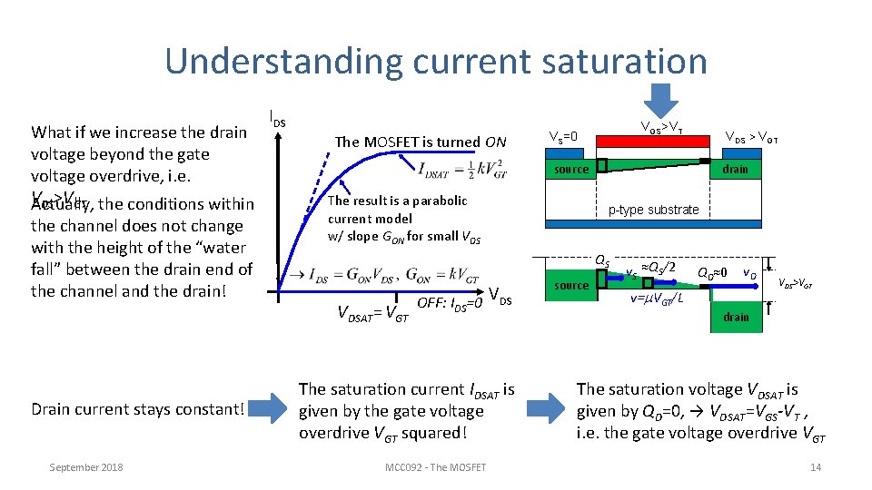
Understanding current saturation What if we increase the drain voltage beyond the gate voltage overdrive, i. e. V DS>VGT the conditions within Actually, the channel does not change with the height of the “water fall” between the drain end of the channel and the drain! Drain current stays constant! September 2018 IDS The MOSFET is turned ON and a current that appears to be proportional to VDS The result a parabolic starts toisflow VGS>VT VS=0 drain source p-type substrate current model w/ slope GON for small VDS QS VDSAT= VGT OFF: IDS=0 VDS The saturation current IDSAT is given by the gate voltage overdrive VGT squared! MCC 092 - The MOSFET VDS > VGT source v. S ≈QS/2 QD≈0 v. D v=m. VGT/L VDS>VGT drain The saturation voltage VDSAT is given by QD=0, → VDSAT=VGS-VT , i. e. the gate voltage overdrive VGT 14

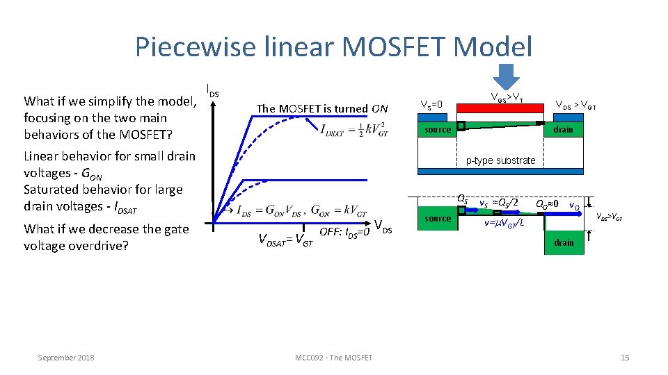
Piecewise linear MOSFET Model What if we simplify the model, focusing on the two main behaviors of the MOSFET? Linear behavior for small drain voltages - GON Saturated behavior for large drain voltages - IDSAT What if we decrease the gate voltage overdrive? September 2018 IDS The MOSFET is turned ON and a current that appears to be proportional to VDS starts to flow VGS>VT VS=0 drain source p-type substrate QSS VDSAT= VGT OFF: IDS=0 MCC 092 - The MOSFET VDS > VGT source ≈QSS/2 /2 vv. S ≈Q QD≈0 ≈0 vv. D Q S D D v=mm. VVGT/L /L v= VDS>VGT GT drain 15

MOSFET output and transfer characteristics IDS The MOSFET is turned ON and for but a current each gate thatvoltage appears to be proportional there is a maximumto VDS starts tothat current flowthe MOSFET can sink or deliver OFF: IDS=0 VDSAT= VGT Output characteristics VDS VGT gate voltage overdrive VGT 2 gate voltage overdrive VT VDD VGS Transfer characteristics The MOSFET is basically a “square-law” device! September 2018 MCC 092 - The MOSFET 16

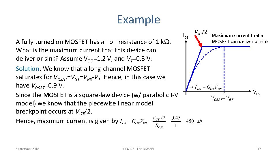
Example A fully turned on MOSFET has an on resistance of 1 k. W. What is the maximum current that this device can deliver or sink? Assume VDD=1. 2 V, and VT=0. 3 V. Solution: We know that a long-channel MOSFET saturates for VDSAT=VGS-VT. Hence, in this case we have VDSAT=0. 9 V. Since the MOSFET is a square-law device (w/ parabolic I-V model) we know that the piecewise linear model breakpoint occurs at VGT/2. Hence, maximum current is given by September 2018 MCC 092 - The MOSFET IDS VGT/2 Maximum current that a MOSFET can deliver or sink VDSAT= VGT VDS 17

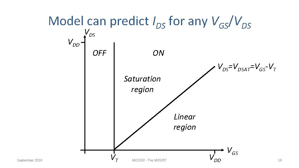
Model can predict IDS for any VGS/VDS VDD VDS OFF ON VDS=VDSAT=VGS-VT Saturation region Linear region September 2018 VT MCC 092 - The MOSFET VDD VGS 18

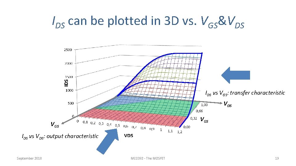
IDS can be plotted in 3 D vs. VGS&VDS IDS vs VGS: transfer characteristic VDS VGS IDS vs VDS: output characteristic September 2018 MCC 092 - The MOSFET 19

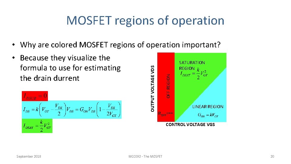
MOSFET regions of operation OFF REGION OUTPUT VOLTAGE VDS • Why are colored MOSFET regions of operation important? • Because they visualize the SATURATION REGION formula to use for estimating the drain durrent LINEAR REGION ROFF=∞ CONTROL VOLTAGE VGS September 2018 MCC 092 - The MOSFET 20

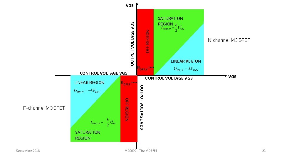
CONTROL VOLTAGE VGS OFF REGION P-channel MOSFET SATURATION REGION September 2018 ROFF, P=∞ N-channel MOSFET LINEAR REGION ROFF, N=∞ CONTROL VOLTAGE VGS OUTPUT VOLTAGE VDS LINEAR REGION SATURATION REGION OFF REGION OUTPUT VOLTAGE VDS MCC 092 - The MOSFET 21

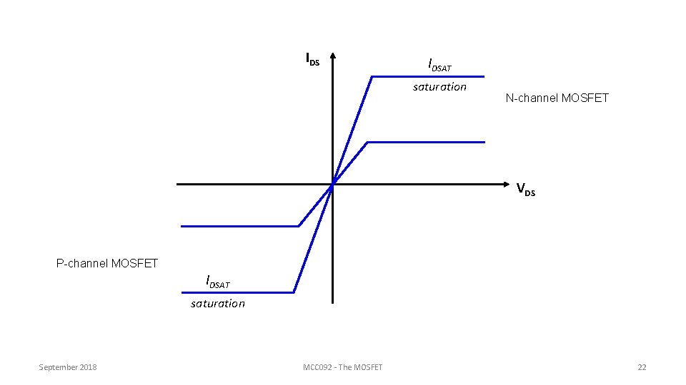
IDS IDSAT saturation N-channel MOSFET VDS P-channel MOSFET IDSAT saturation September 2018 MCC 092 - The MOSFET 22

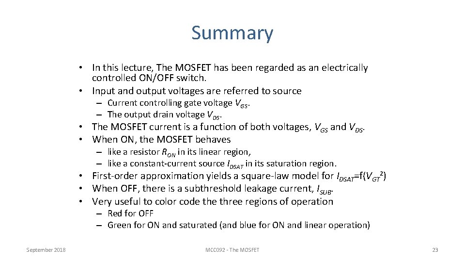
Summary • In this lecture, The MOSFET has been regarded as an electrically controlled ON/OFF switch. • Input and output voltages are referred to source – Current controlling gate voltage VGS. – The output drain voltage VDS. • The MOSFET current is a function of both voltages, VGS and VDS. • When ON, the MOSFET behaves – like a resistor RON in its linear region, – like a constant-current source IDSAT in its saturation region. • First-order approximation yields a square-law model for IDSAT=f(VGT 2) • When OFF, there is a subthreshold leakage current, ISUB. • Very useful to color code three regions of operation – Red for OFF – Green for ON and saturated (and blue for ON and linear operation) September 2018 MCC 092 - The MOSFET 23

Equivalent electrical two-port circuit model CGD G/2 In the linear region, the VGS VDS capacitance splits equally CGS G/2 VSS GON Model for linear device VGS CGS ⅔C G VSS between source and drain CGD=0 The distributed gate to channel capacitance must be lumped to the available ckt nodes, i. e. to source and drain VDS VSS CG VDS IDSAT VSS Model for saturated device In the saturation region, the capacitance tilts towards the source! The field-effect upon which the operation of a MOSFET relies, gives the MOSFET a capacitive input! September 2018 VGS VSS Reff VSS “Average” model during switching of device output Q: Why use CGS=CG and not CGS=⅔CG? A: Integers are easier to handle and there are parasitic overlap and fringing field caps there to motivate the approximation! MCC 092 - The MOSFET 24

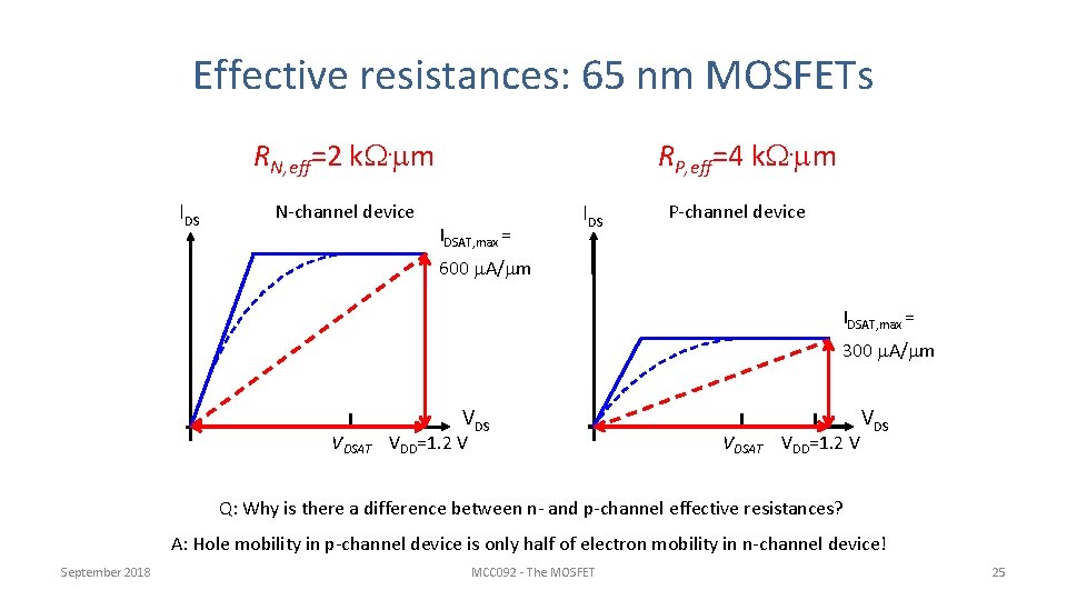
Effective resistances: 65 nm MOSFETs RP, eff=4 k. W. mm RN, eff=2 k. W. mm IDS N-channel device IDSAT, max = IDS P-channel device 600 m. A/mm IDSAT, max = 300 m. A/mm VDSAT VDD=1. 2 V VDS Q: Why is there a difference between n- and p-channel effective resistances? A: Hole mobility in p-channel device is only half of electron mobility in n-channel device! September 2018 MCC 092 - The MOSFET 25

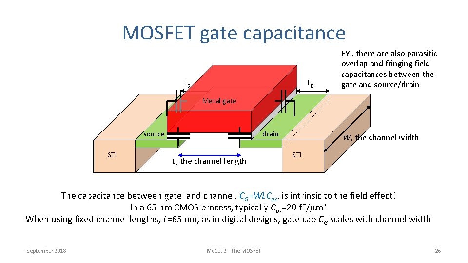
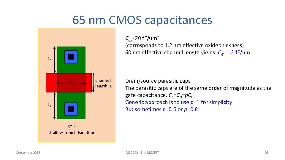
MOSFET gate capacitance LD LS FYI, there also parasitic overlap and fringing field capacitances between the gate and source/drain Metal gate source STI drain L, the channel length W, the channel width STI The capacitance between gate and channel, CG=WLCox, is intrinsic to the field effect! In a 65 nm CMOS process, typically Cox=20 f. F/mm 2 When using fixed channel lengths, L=65 nm, as in digital designs, gate cap CG scales with channel width September 2018 MCC 092 - The MOSFET 26

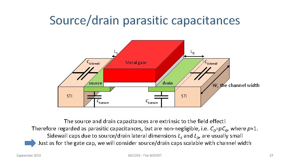
Source/drain parasitic capacitances LD LS Csidewall source STI Cbottom Csidewall Metal gate drain Cbottom W, the channel width STI The source and drain capacitances are extrinsic to the field effect! Therefore regarded as parasitic capacitances, but are non-negligible, i. e. CD=p. CG, where p≈1. Sidewall caps due to source/drain lateral dimensions LS and LD, are usually small Just as for the gate cap, we will consider source/drain caps scalable with channel width September 2018 MCC 092 - The MOSFET 27

65 nm CMOS capacitances Cox≈20 f. F/um 2 (corresponds to 1. 2 nm effective oxide thickness) 60 nm effective channel length yields: CG=1. 2 f. F/um LD W LS channel length, L Drain/source parasitic caps The parasitic caps are of the same order of magnitude as the gate capacitance, CS=CD=p. CG Generic approach is to use p=1 for simplicity But sometimes p=0. 5 or p=0. 8! STI: shallow trench isolation September 2018 MCC 092 - The MOSFET 28

Equivalent electrical two-port circuit model CGD G/2 VGS VDS CGGS/2 VSS GON Model for linear device VGS CG CGD=0 CD The distributed gate to channel capacitance must be lumped to the available ckt nodes, i. e. source and drain VGS VSS CG VDS IDSAT VSS Model for saturated device VDS CD VSS Reff VSS CD VSS “Average” model during switching of device output where Cox is the gate insulator capacitance per unit area, typically 20 f. F/mm 2 September 2018 where p is a certain fraction of the gate capacitance, typically p=1 MCC 092 - The MOSFET 29

The MOSFET in detail • A number of textbooks treat MOSFET models in great detail, including their physical background and shortcomings due to short-channel effects in nanoscale devices September 2018 MCC 092 - The MOSFET 30

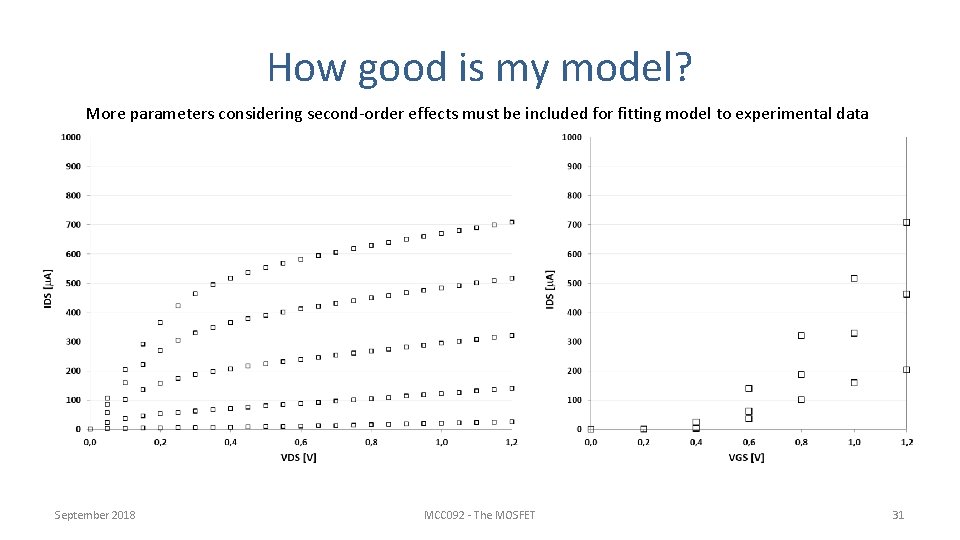
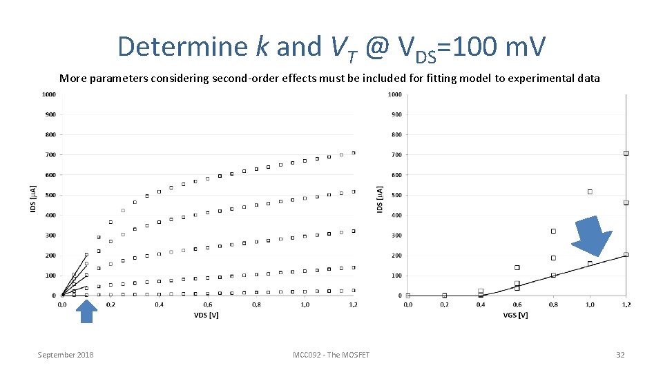
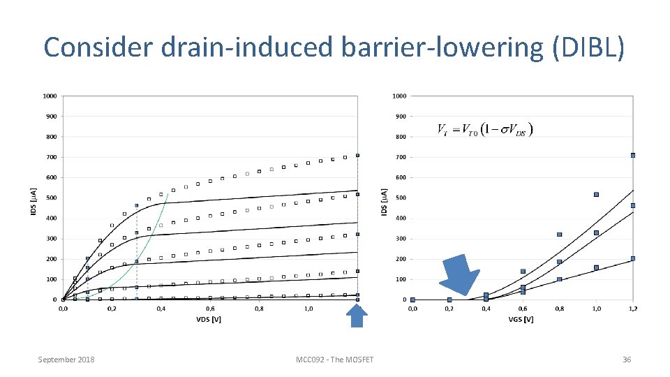
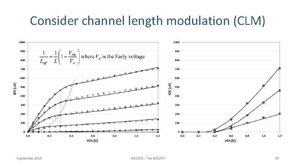
How good is my model? More parameters considering second-order effects must be included for fitting model to experimental data September 2018 MCC 092 - The MOSFET 31

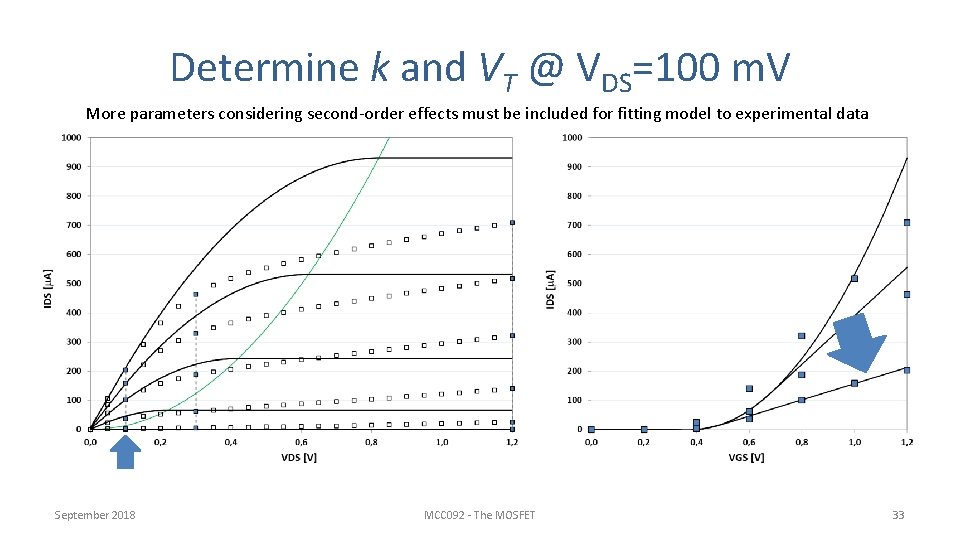
Determine k and VT @ VDS=100 m. V More parameters considering second-order effects must be included for fitting model to experimental data September 2018 MCC 092 - The MOSFET 32

Determine k and VT @ VDS=100 m. V More parameters considering second-order effects must be included for fitting model to experimental data September 2018 MCC 092 - The MOSFET 33

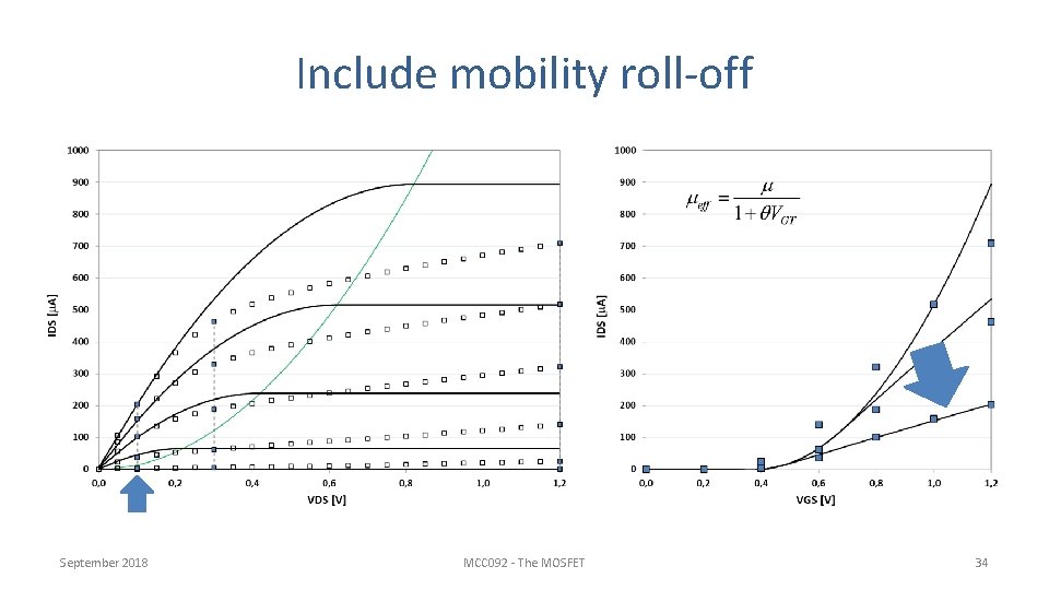
Include mobility roll-off September 2018 MCC 092 - The MOSFET 34

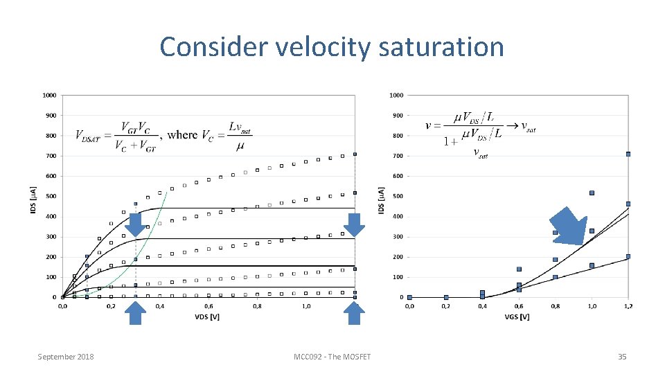
Consider velocity saturation September 2018 MCC 092 - The MOSFET 35

Consider drain-induced barrier-lowering (DIBL) September 2018 MCC 092 - The MOSFET 36

Consider channel length modulation (CLM) September 2018 MCC 092 - The MOSFET 37

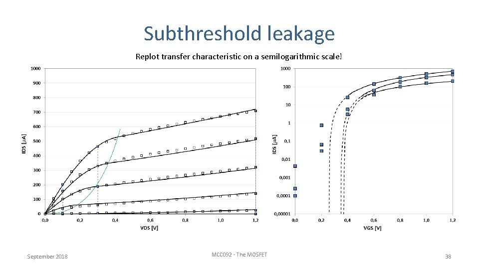
Subthreshold leakage Replot transfer characteristic on a semilogarithmic scale! September 2018 MCC 092 - The MOSFET 38

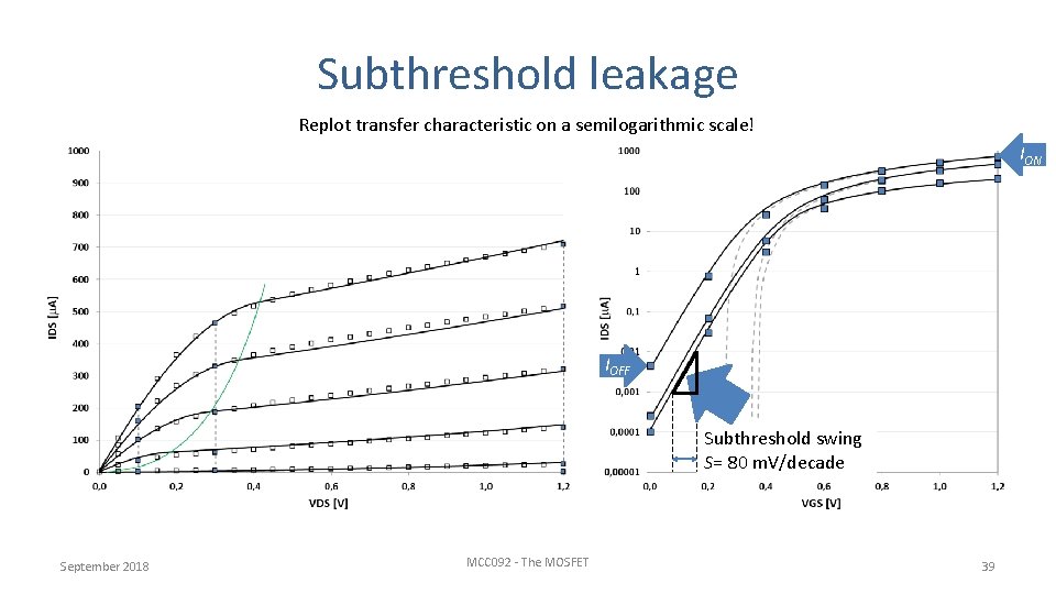
Subthreshold leakage Replot transfer characteristic on a semilogarithmic scale! ION IOFF Subthreshold swing S= 80 m. V/decade September 2018 MCC 092 - The MOSFET 39

Conclusion In this lecture, we started considering MOSFET static properties • Three regions of operation – Two ON regions: linear or saturated – One OFF region: subthreshold In second half of lecture we also considered dynamic properties • The intrinsic gate capacitance • The extrinsic, or parasitic drain capacitance We came up with a two-port model including both static circuit elements (resistor or current-source), and dynamic elements, i. e. capacitances! September 2018 MCC 092 - The MOSFET 40