18 740640 Computer Architecture Lecture 8 Main Memory










![Ramulator: A Fast and Extensible DRAM Simulator [IEEE Comp Arch Letters’ 15] 139 Ramulator: A Fast and Extensible DRAM Simulator [IEEE Comp Arch Letters’ 15] 139](https://slidetodoc.com/presentation_image_h2/d08edf6df9695906ae93866a8e50ef25/image-139.jpg)
- Slides: 144

18 -740/640 Computer Architecture Lecture 8: Main Memory System Prof. Onur Mutlu Carnegie Mellon University Fall 2015, 9/28/2015

Required Readings Ø Required Reading Assignment: • Sec. 1 & 3 of B. Jacob, “The Memory System: You Can’t Avoid It, You Can’t Ignore It, You Can’t Fake It, ” Synthesis Lectures on Computer Architecture, 2009. Ø Recommended References: • O. Mutlu and L. Subramanian, “Research Problems and Opportunities in Memory Systems, ” Supercomputing Frontiers and Innovations, 2015. • Lee et al. , “Phase Change Technology and the Future of Main Memory, ” IEEE Micro, Jan/Feb 2010. • Y. Kim, W. Yang, O. Mutlu, “Ramulator: A Fast and Extensible DRAM Simulator, ” IEEE Computer Architecture Letters, May 2015. 2

State-of-the-art in Main Memory… n Onur Mutlu and Lavanya Subramanian, "Research Problems and Opportunities in Memory Systems" Invited Article in Supercomputing Frontiers and Innovations (SUPERFRI), 2015. 3

Recommended Readings on DRAM Organization and Operation Basics q q n Sections 1 and 2 of: Lee et al. , “Tiered-Latency DRAM: A Low Latency and Low Cost DRAM Architecture, ” HPCA 2013. http: //users. ece. cmu. edu/~omutlu/pub/tldram_hpca 13. pdf Sections 1 and 2 of Kim et al. , “A Case for Subarray-Level Parallelism (SALP) in DRAM, ” ISCA 2012. http: //users. ece. cmu. edu/~omutlu/pub/salp-dram_isca 12. pdf DRAM Refresh Basics q Sections 1 and 2 of Liu et al. , “RAIDR: Retention-Aware Intelligent DRAM Refresh, ” ISCA 2012. http: //users. ece. cmu. edu/~omutlu/pub/raidr-dramrefresh_isca 12. pdf 4

Simulating Main Memory n n n How to evaluate future main memory systems? An open-source simulator and its brief description Yoongu Kim, Weikun Yang, and Onur Mutlu, "Ramulator: A Fast and Extensible DRAM Simulator" IEEE Computer Architecture Letters (CAL), March 2015. [Source Code] 5

Why Is Main Memory So Important Especially Today?

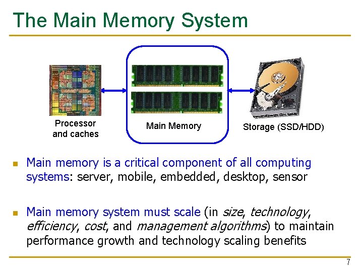
The Main Memory System Processor and caches n n Main Memory Storage (SSD/HDD) Main memory is a critical component of all computing systems: server, mobile, embedded, desktop, sensor Main memory system must scale (in size, technology, efficiency, cost, and management algorithms) to maintain performance growth and technology scaling benefits 7

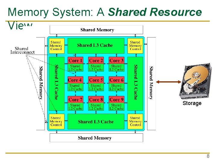
Memory System: A Shared Resource View Storage 8

State of the Main Memory System n Recent technology, architecture, and application trends q q n n n lead to new requirements exacerbate old requirements DRAM and memory controllers, as we know them today, are (will be) unlikely to satisfy all requirements Some emerging non-volatile memory technologies (e. g. , PCM) enable new opportunities: memory+storage merging We need to rethink the main memory system q q to fix DRAM issues and enable emerging technologies to satisfy all requirements 9

Major Trends Affecting Main Memory (I) n Need for main memory capacity, bandwidth, Qo. S increasing n Main memory energy/power is a key system design concern n DRAM technology scaling is ending 10

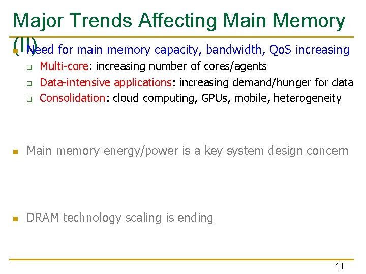
Major Trends Affecting Main Memory (II) n Need for main memory capacity, bandwidth, Qo. S increasing q q q Multi-core: increasing number of cores/agents Data-intensive applications: increasing demand/hunger for data Consolidation: cloud computing, GPUs, mobile, heterogeneity n Main memory energy/power is a key system design concern n DRAM technology scaling is ending 11

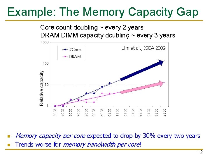
Example: The Memory Capacity Gap Core count doubling ~ every 2 years DRAM DIMM capacity doubling ~ every 3 years Lim et al. , ISCA 2009 n n Memory capacity per core expected to drop by 30% every two years Trends worse for memory bandwidth per core! 12

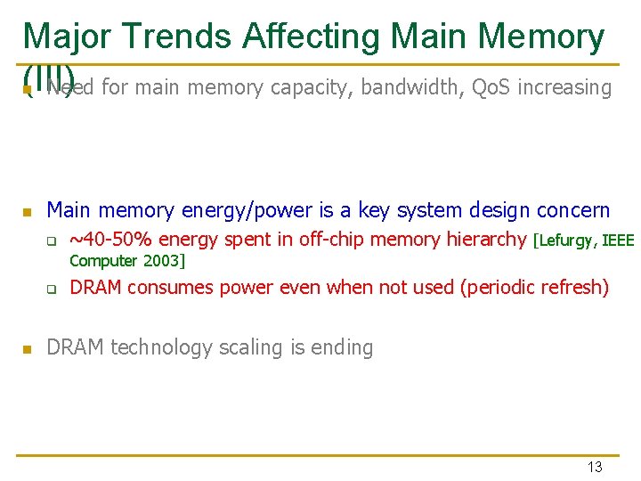
Major Trends Affecting Main Memory (III) n Need for main memory capacity, bandwidth, Qo. S increasing n Main memory energy/power is a key system design concern q ~40 -50% energy spent in off-chip memory hierarchy [Lefurgy, IEEE Computer 2003] q n DRAM consumes power even when not used (periodic refresh) DRAM technology scaling is ending 13

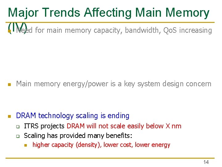
Major Trends Affecting Main Memory (IV) n Need for main memory capacity, bandwidth, Qo. S increasing n Main memory energy/power is a key system design concern n DRAM technology scaling is ending q q ITRS projects DRAM will not scale easily below X nm Scaling has provided many benefits: n higher capacity (density), lower cost, lower energy 14

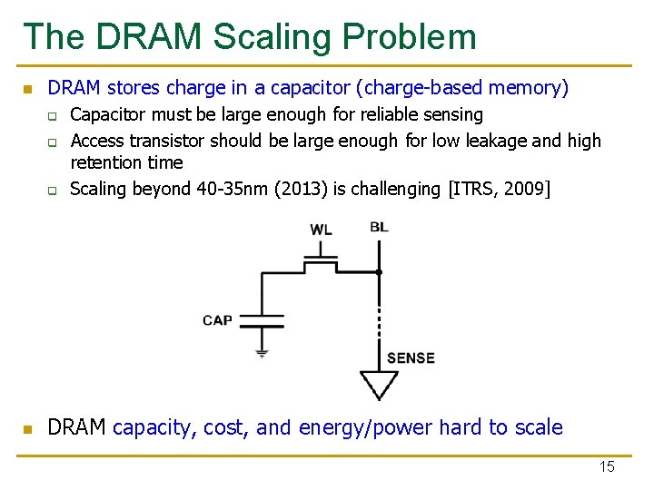
The DRAM Scaling Problem n DRAM stores charge in a capacitor (charge-based memory) q q q n Capacitor must be large enough for reliable sensing Access transistor should be large enough for low leakage and high retention time Scaling beyond 40 -35 nm (2013) is challenging [ITRS, 2009] DRAM capacity, cost, and energy/power hard to scale 15

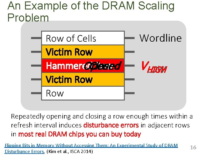
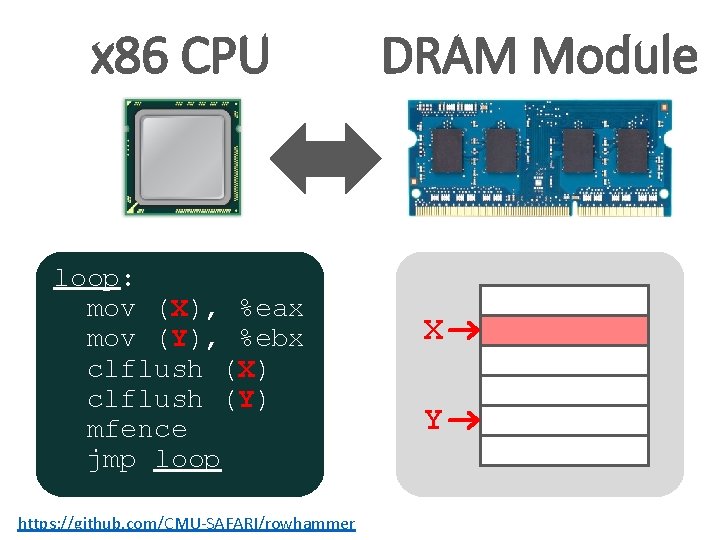
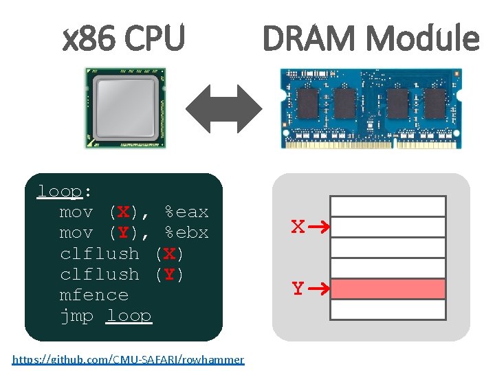
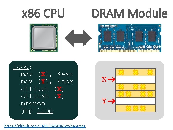
An Example of the DRAM Scaling Problem Row of Cells Victim Row Hammered Row Opened Closed Victim Row Row Wordline VHIGH LOW Repeatedly opening and closing a row enough times within a refresh interval induces disturbance errors in adjacent rows in most real DRAM chips you can buy today Flipping Bits in Memory Without Accessing Them: An Experimental Study of DRAM Disturbance Errors, (Kim et al. , ISCA 2014) 16

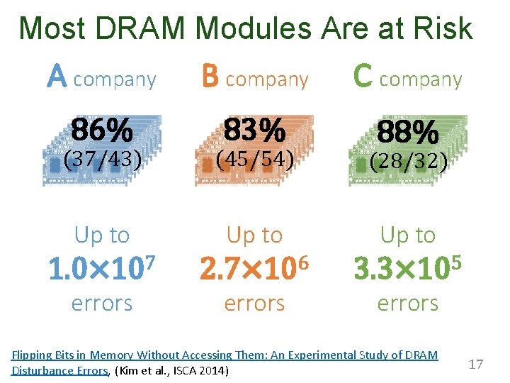
Most DRAM Modules Are at Risk A company B company C company 86% 83% (37/43) (45/54) 88% (28/32) Up to 7 1. 0× 10 6 2. 7× 10 5 3. 3× 10 errors Flipping Bits in Memory Without Accessing Them: An Experimental Study of DRAM Disturbance Errors, (Kim et al. , ISCA 2014) 17

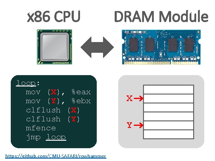
x 86 CPU loop: mov (X), %eax mov (Y), %ebx clflush (X) clflush (Y) mfence jmp loop https: //github. com/CMU-SAFARI/rowhammer DRAM Module X Y

x 86 CPU loop: mov (X), %eax mov (Y), %ebx clflush (X) clflush (Y) mfence jmp loop https: //github. com/CMU-SAFARI/rowhammer DRAM Module X Y

x 86 CPU loop: mov (X), %eax mov (Y), %ebx clflush (X) clflush (Y) mfence jmp loop https: //github. com/CMU-SAFARI/rowhammer DRAM Module X Y

x 86 CPU loop: mov (X), %eax mov (Y), %ebx clflush (X) clflush (Y) mfence jmp loop https: //github. com/CMU-SAFARI/rowhammer DRAM Module X Y

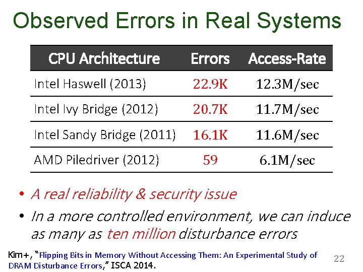
Observed Errors in Real Systems CPU Architecture Errors Access-Rate Intel Haswell (2013) 22. 9 K 12. 3 M/sec Intel Ivy Bridge (2012) 20. 7 K 11. 7 M/sec Intel Sandy Bridge (2011) 16. 1 K 11. 6 M/sec 59 6. 1 M/sec AMD Piledriver (2012) • A real reliability & security issue • In a more controlled environment, we can induce as many as ten million disturbance errors Kim+, “Flipping Bits in Memory Without Accessing Them: An Experimental Study of DRAM Disturbance Errors, ” ISCA 2014. 22

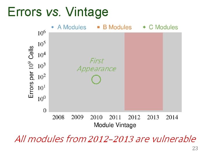
Errors vs. Vintage First Appearance All modules from 2012– 2013 are vulnerable 23

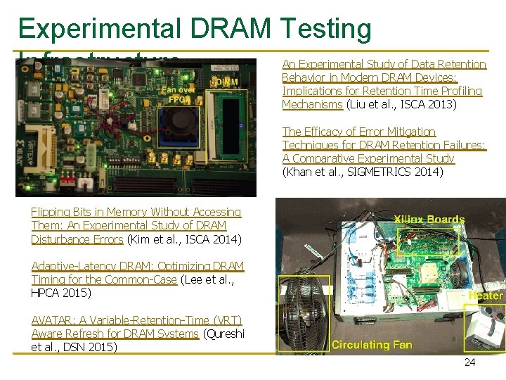
Experimental DRAM Testing Infrastructure An Experimental Study of Data Retention Behavior in Modern DRAM Devices: Implications for Retention Time Profiling Mechanisms (Liu et al. , ISCA 2013) The Efficacy of Error Mitigation Techniques for DRAM Retention Failures: A Comparative Experimental Study (Khan et al. , SIGMETRICS 2014) Flipping Bits in Memory Without Accessing Them: An Experimental Study of DRAM Disturbance Errors (Kim et al. , ISCA 2014) Adaptive-Latency DRAM: Optimizing DRAM Timing for the Common-Case (Lee et al. , HPCA 2015) AVATAR: A Variable-Retention-Time (VRT) Aware Refresh for DRAM Systems (Qureshi et al. , DSN 2015) 24

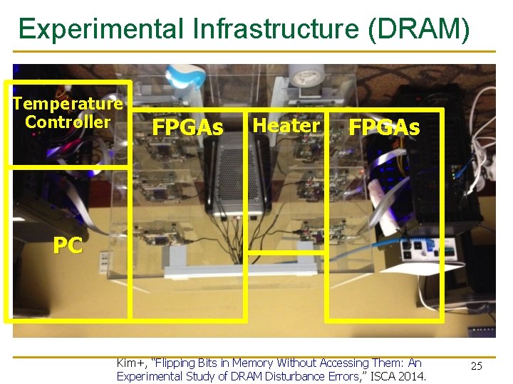
Experimental Infrastructure (DRAM) Temperature Controller FPGAs Heater FPGAs PC Kim+, “Flipping Bits in Memory Without Accessing Them: An Experimental Study of DRAM Disturbance Errors, ” ISCA 2014. 25

Row. Hammer Characterization Results 1. Most Modules Are at Risk 2. Errors vs. Vintage 3. Error = Charge Loss 4. Adjacency: Aggressor & Victim 5. Sensitivity Studies 6. Other Results in Paper 7. Solution Space Flipping Bits in Memory Without Accessing Them: An Experimental Study of DRAM Disturbance Errors, (Kim et al. , ISCA 2014) 26

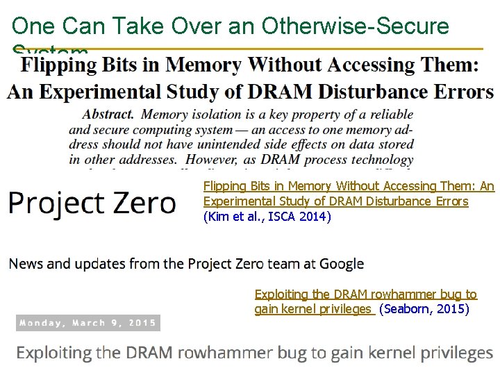
One Can Take Over an Otherwise-Secure System Flipping Bits in Memory Without Accessing Them: An Experimental Study of DRAM Disturbance Errors (Kim et al. , ISCA 2014) Exploiting the DRAM rowhammer bug to gain kernel privileges (Seaborn, 2015) 27

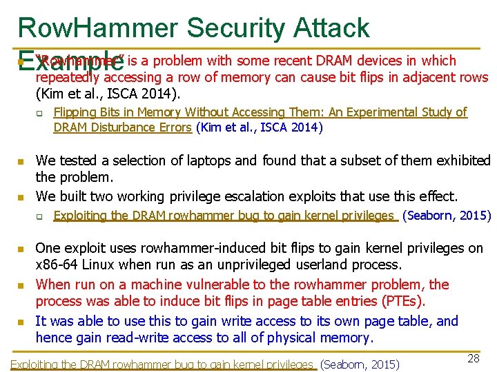
Row. Hammer Security Attack “Rowhammer” is a problem with some recent DRAM devices in which Example repeatedly accessing a row of memory can cause bit flips in adjacent rows n (Kim et al. , ISCA 2014). q n n We tested a selection of laptops and found that a subset of them exhibited the problem. We built two working privilege escalation exploits that use this effect. q n n n Flipping Bits in Memory Without Accessing Them: An Experimental Study of DRAM Disturbance Errors (Kim et al. , ISCA 2014) Exploiting the DRAM rowhammer bug to gain kernel privileges (Seaborn, 2015) One exploit uses rowhammer-induced bit flips to gain kernel privileges on x 86 -64 Linux when run as an unprivileged userland process. When run on a machine vulnerable to the rowhammer problem, the process was able to induce bit flips in page table entries (PTEs). It was able to use this to gain write access to its own page table, and hence gain read-write access to all of physical memory. Exploiting the DRAM rowhammer bug to gain kernel privileges (Seaborn, 2015) 28

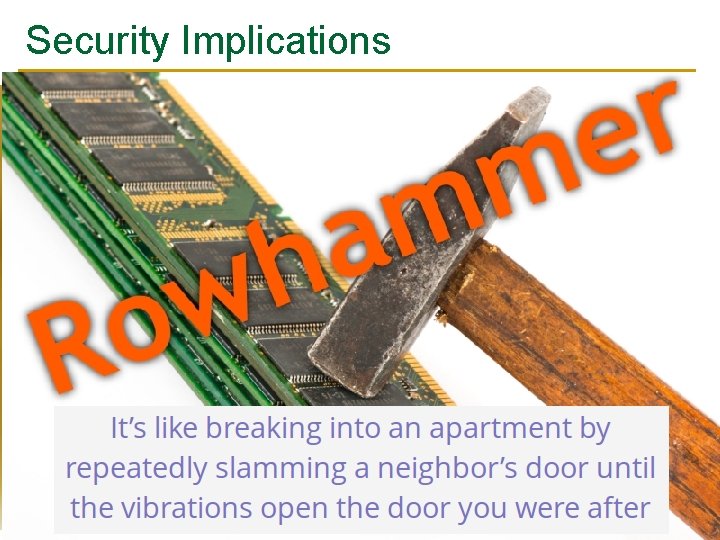
Security Implications 29

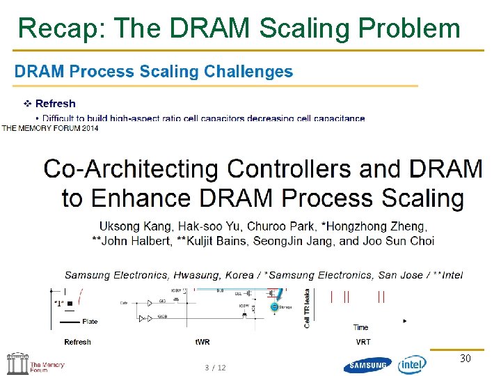
Recap: The DRAM Scaling Problem 30

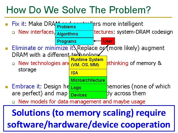
How Do We Solve The Problem? n Fix it: Make DRAMProblems and controllers more intelligent q New interfaces, Algorithms functions, architectures: system-DRAM codesign Programs n User Eliminate or minimize it: Replace or (more likely) augment DRAM with a different technology q New technologies storage Runtime System and(VM, system-wide OS, MM) rethinking of memory & ISA Microarchitecture n Embrace it: Design heterogeneous memories (none of which Logic are perfect) and map data intelligently across them Devices q New models for data management and maybe usage Solutions (to memory scaling) require n … software/hardware/device cooperation 31

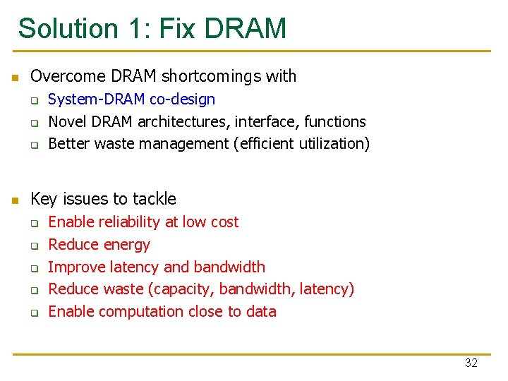
Solution 1: Fix DRAM n Overcome DRAM shortcomings with q q q n System-DRAM co-design Novel DRAM architectures, interface, functions Better waste management (efficient utilization) Key issues to tackle q q q Enable reliability at low cost Reduce energy Improve latency and bandwidth Reduce waste (capacity, bandwidth, latency) Enable computation close to data 32

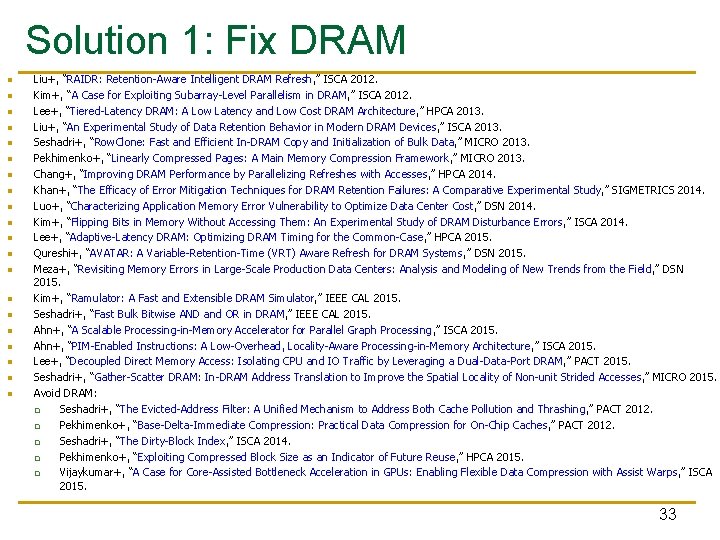
Solution 1: Fix DRAM n n n n n Liu+, “RAIDR: Retention-Aware Intelligent DRAM Refresh, ” ISCA 2012. Kim+, “A Case for Exploiting Subarray-Level Parallelism in DRAM, ” ISCA 2012. Lee+, “Tiered-Latency DRAM: A Low Latency and Low Cost DRAM Architecture, ” HPCA 2013. Liu+, “An Experimental Study of Data Retention Behavior in Modern DRAM Devices, ” ISCA 2013. Seshadri+, “Row. Clone: Fast and Efficient In-DRAM Copy and Initialization of Bulk Data, ” MICRO 2013. Pekhimenko+, “Linearly Compressed Pages: A Main Memory Compression Framework, ” MICRO 2013. Chang+, “Improving DRAM Performance by Parallelizing Refreshes with Accesses, ” HPCA 2014. Khan+, “The Efficacy of Error Mitigation Techniques for DRAM Retention Failures: A Comparative Experimental Study, ” SIGMETRICS 2014. Luo+, “Characterizing Application Memory Error Vulnerability to Optimize Data Center Cost, ” DSN 2014. Kim+, “Flipping Bits in Memory Without Accessing Them: An Experimental Study of DRAM Disturbance Errors, ” ISCA 2014. Lee+, “Adaptive-Latency DRAM: Optimizing DRAM Timing for the Common-Case, ” HPCA 2015. Qureshi+, “AVATAR: A Variable-Retention-Time (VRT) Aware Refresh for DRAM Systems, ” DSN 2015. Meza+, “Revisiting Memory Errors in Large-Scale Production Data Centers: Analysis and Modeling of New Trends from the Field, ” DSN 2015. Kim+, “Ramulator: A Fast and Extensible DRAM Simulator, ” IEEE CAL 2015. Seshadri+, “Fast Bulk Bitwise AND and OR in DRAM, ” IEEE CAL 2015. Ahn+, “A Scalable Processing-in-Memory Accelerator for Parallel Graph Processing, ” ISCA 2015. Ahn+, “PIM-Enabled Instructions: A Low-Overhead, Locality-Aware Processing-in-Memory Architecture, ” ISCA 2015. Lee+, “Decoupled Direct Memory Access: Isolating CPU and IO Traffic by Leveraging a Dual-Data-Port DRAM, ” PACT 2015. Seshadri+, “Gather-Scatter DRAM: In-DRAM Address Translation to Improve the Spatial Locality of Non-unit Strided Accesses, ” MICRO 2015. Avoid DRAM: q Seshadri+, “The Evicted-Address Filter: A Unified Mechanism to Address Both Cache Pollution and Thrashing, ” PACT 2012. q Pekhimenko+, “Base-Delta-Immediate Compression: Practical Data Compression for On-Chip Caches, ” PACT 2012. q Seshadri+, “The Dirty-Block Index, ” ISCA 2014. q Pekhimenko+, “Exploiting Compressed Block Size as an Indicator of Future Reuse, ” HPCA 2015. q Vijaykumar+, “A Case for Core-Assisted Bottleneck Acceleration in GPUs: Enabling Flexible Data Compression with Assist Warps, ” ISCA 2015. 33

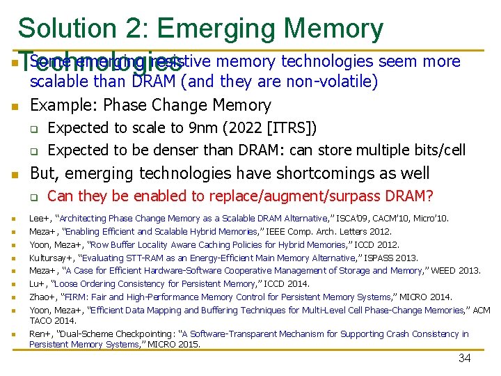
Solution 2: Emerging Memory n. Technologies Some emerging resistive memory technologies seem more n scalable than DRAM (and they are non-volatile) Example: Phase Change Memory q q n But, emerging technologies have shortcomings as well q n n n n n Expected to scale to 9 nm (2022 [ITRS]) Expected to be denser than DRAM: can store multiple bits/cell Can they be enabled to replace/augment/surpass DRAM? Lee+, “Architecting Phase Change Memory as a Scalable DRAM Alternative, ” ISCA’ 09, CACM’ 10, Micro’ 10. Meza+, “Enabling Efficient and Scalable Hybrid Memories, ” IEEE Comp. Arch. Letters 2012. Yoon, Meza+, “Row Buffer Locality Aware Caching Policies for Hybrid Memories, ” ICCD 2012. Kultursay+, “Evaluating STT-RAM as an Energy-Efficient Main Memory Alternative, ” ISPASS 2013. Meza+, “A Case for Efficient Hardware-Software Cooperative Management of Storage and Memory, ” WEED 2013. Lu+, “Loose Ordering Consistency for Persistent Memory, ” ICCD 2014. Zhao+, “FIRM: Fair and High-Performance Memory Control for Persistent Memory Systems, ” MICRO 2014. Yoon, Meza+, “Efficient Data Mapping and Buffering Techniques for Multi-Level Cell Phase-Change Memories, ” ACM TACO 2014. Ren+, “Dual-Scheme Checkpointing: “A Software-Transparent Mechanism for Supporting Crash Consistency in Persistent Memory Systems, ” MICRO 2015. 34

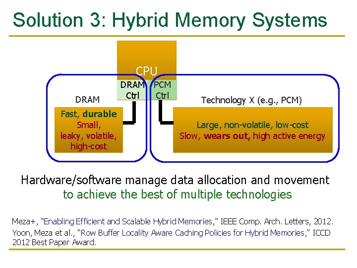
Solution 3: Hybrid Memory Systems CPU DRAM Fast, durable Small, leaky, volatile, high-cost DRAM Ctrl PCM Ctrl Technology X (e. g. , PCM) Large, non-volatile, low-cost Slow, wears out, high active energy Hardware/software manage data allocation and movement to achieve the best of multiple technologies Meza+, “Enabling Efficient and Scalable Hybrid Memories, ” IEEE Comp. Arch. Letters, 2012. Yoon, Meza et al. , “Row Buffer Locality Aware Caching Policies for Hybrid Memories, ” ICCD 2012 Best Paper Award.

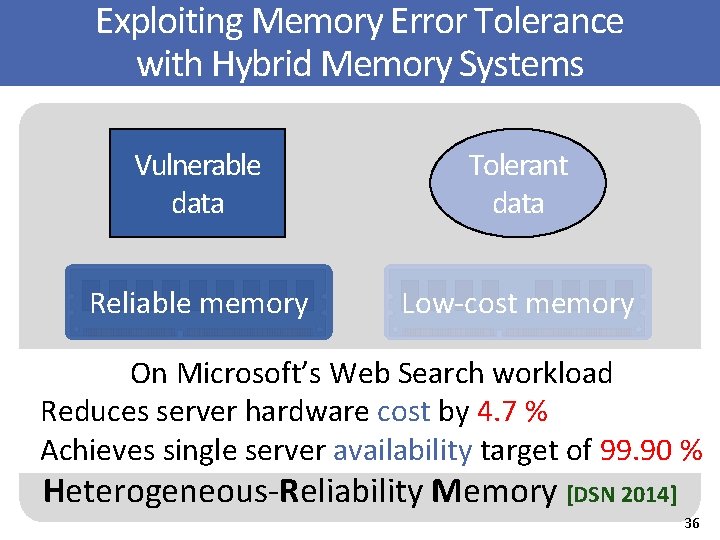
Memory error vulnerability Exploiting Memory Error Tolerance with Hybrid Memory Systems Vulnerable data Tolerant data Reliable memory Low-cost memory Onprotected Microsoft’s Web • Search Vulnerable • ECC No. ECCworkload or Tolerant Parity data Reduces server hardware cost by 4. 7 % data • Well-tested chips • Less-tested chips Achieves single server availability target of 99. 90 % App/Data A App/Data B App/Data C Heterogeneous-Reliability Memory [DSN 2014] 36

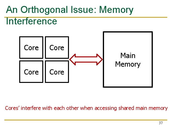
An Orthogonal Issue: Memory Interference Core Main Memory Cores’ interfere with each other when accessing shared main memory 37

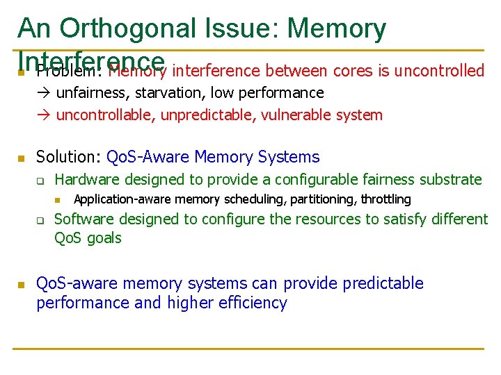
An Orthogonal Issue: Memory Interference n Problem: Memory interference between cores is uncontrolled unfairness, starvation, low performance uncontrollable, unpredictable, vulnerable system n Solution: Qo. S-Aware Memory Systems q Hardware designed to provide a configurable fairness substrate n q n Application-aware memory scheduling, partitioning, throttling Software designed to configure the resources to satisfy different Qo. S goals Qo. S-aware memory systems can provide predictable performance and higher efficiency

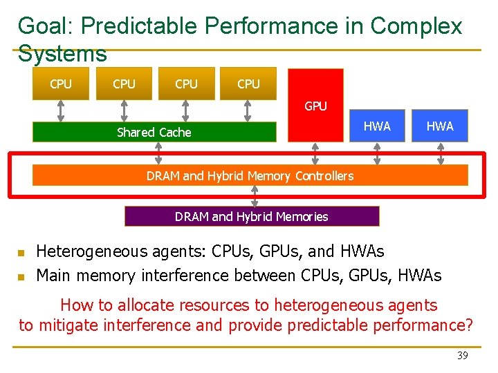
Goal: Predictable Performance in Complex Systems CPU CPU GPU Shared Cache HWA DRAM and Hybrid Memory Controllers DRAM and Hybrid Memories n n Heterogeneous agents: CPUs, GPUs, and HWAs Main memory interference between CPUs, GPUs, HWAs How to allocate resources to heterogeneous agents to mitigate interference and provide predictable performance? 39

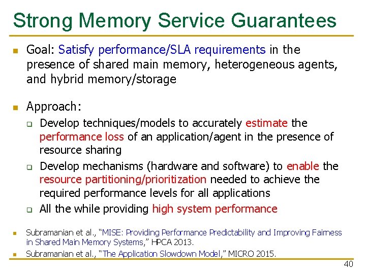
Strong Memory Service Guarantees n n Goal: Satisfy performance/SLA requirements in the presence of shared main memory, heterogeneous agents, and hybrid memory/storage Approach: q q q n n Develop techniques/models to accurately estimate the performance loss of an application/agent in the presence of resource sharing Develop mechanisms (hardware and software) to enable the resource partitioning/prioritization needed to achieve the required performance levels for all applications All the while providing high system performance Subramanian et al. , “MISE: Providing Performance Predictability and Improving Fairness in Shared Main Memory Systems, ” HPCA 2013. Subramanian et al. , “The Application Slowdown Model, ” MICRO 2015. 40

Main Memory Fundamentals

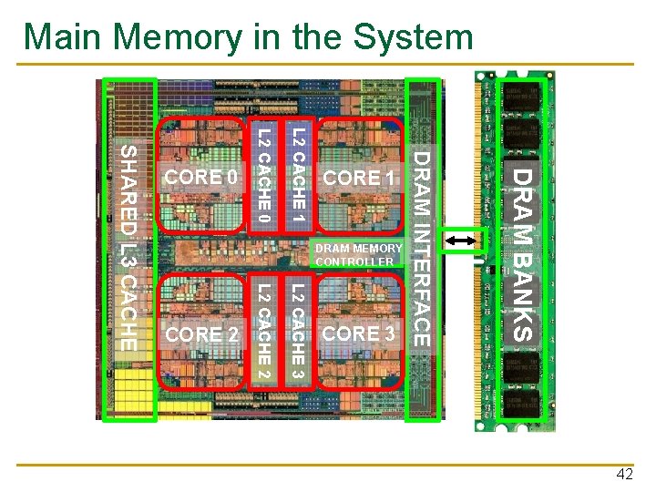
Main Memory in the System DRAM BANKS L 2 CACHE 3 L 2 CACHE 2 SHARED L 3 CACHE DRAM MEMORY CONTROLLER DRAM INTERFACE L 2 CACHE 1 L 2 CACHE 0 CORE 3 CORE 2 CORE 1 CORE 0 42

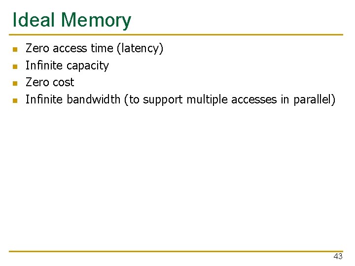
Ideal Memory n n Zero access time (latency) Infinite capacity Zero cost Infinite bandwidth (to support multiple accesses in parallel) 43

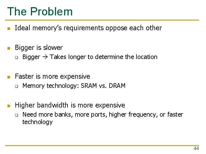
The Problem n Ideal memory’s requirements oppose each other n Bigger is slower q n Faster is more expensive q n Bigger Takes longer to determine the location Memory technology: SRAM vs. DRAM Higher bandwidth is more expensive q Need more banks, more ports, higher frequency, or faster technology 44

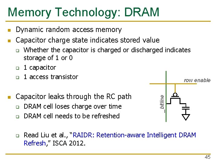
Memory Technology: DRAM n Dynamic random access memory Capacitor charge state indicates stored value q q q n Whether the capacitor is charged or discharged indicates storage of 1 or 0 1 capacitor 1 access transistor row enable Capacitor leaks through the RC path q q q DRAM cell loses charge over time DRAM cell needs to be refreshed _bitline n Read Liu et al. , “RAIDR: Retention-aware Intelligent DRAM Refresh, ” ISCA 2012. 45

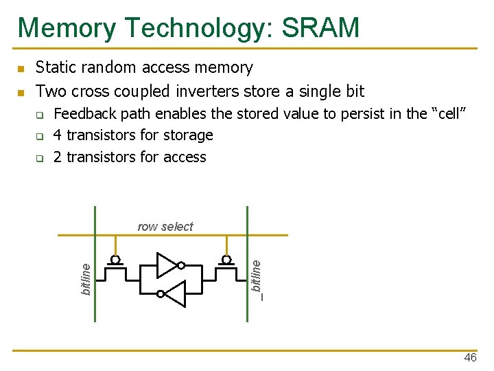
Memory Technology: SRAM q q q Feedback path enables the stored value to persist in the “cell” 4 transistors for storage 2 transistors for access row select _bitline n Static random access memory Two cross coupled inverters store a single bitline n 46

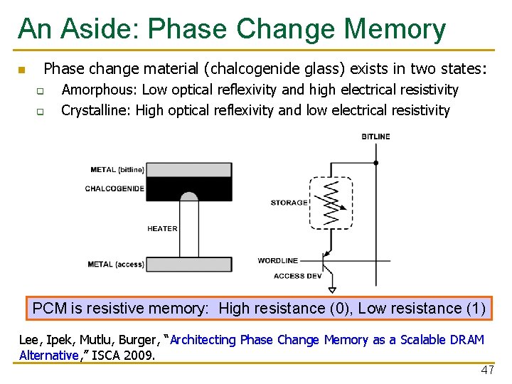
An Aside: Phase Change Memory n Phase change material (chalcogenide glass) exists in two states: q q Amorphous: Low optical reflexivity and high electrical resistivity Crystalline: High optical reflexivity and low electrical resistivity PCM is resistive memory: High resistance (0), Low resistance (1) Lee, Ipek, Mutlu, Burger, “Architecting Phase Change Memory as a Scalable DRAM Alternative, ” ISCA 2009. 47

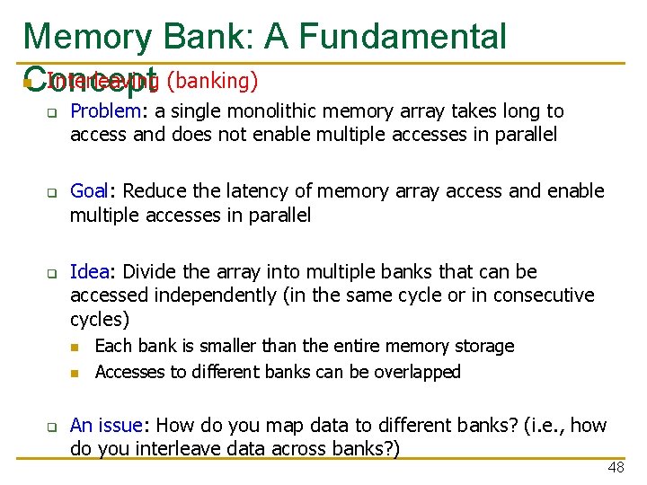
Memory Bank: A Fundamental n Interleaving (banking) Concept q q q Problem: a single monolithic memory array takes long to access and does not enable multiple accesses in parallel Goal: Reduce the latency of memory array access and enable multiple accesses in parallel Idea: Divide the array into multiple banks that can be accessed independently (in the same cycle or in consecutive cycles) n n q Each bank is smaller than the entire memory storage Accesses to different banks can be overlapped An issue: How do you map data to different banks? (i. e. , how do you interleave data across banks? ) 48

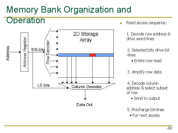
Memory Bank Organization and Operation Read access sequence: n 1. Decode row address & drive word-lines 2. Selected bits drive bit -lines • Entire row read 3. Amplify row data 4. Decode column address & select subset of row • Send to output 5. Precharge bit-lines • For next access 49

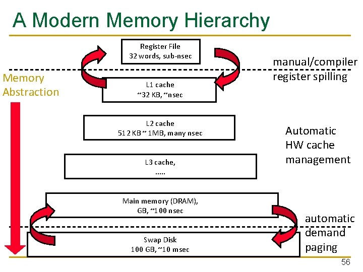
Why Memory Hierarchy? n We want both fast and large n But we cannot achieve both with a single level of memory n Idea: Have multiple levels of storage (progressively bigger and slower as the levels are farther from the processor) and ensure most of the data the processor needs is kept in the fast(er) level(s) 50

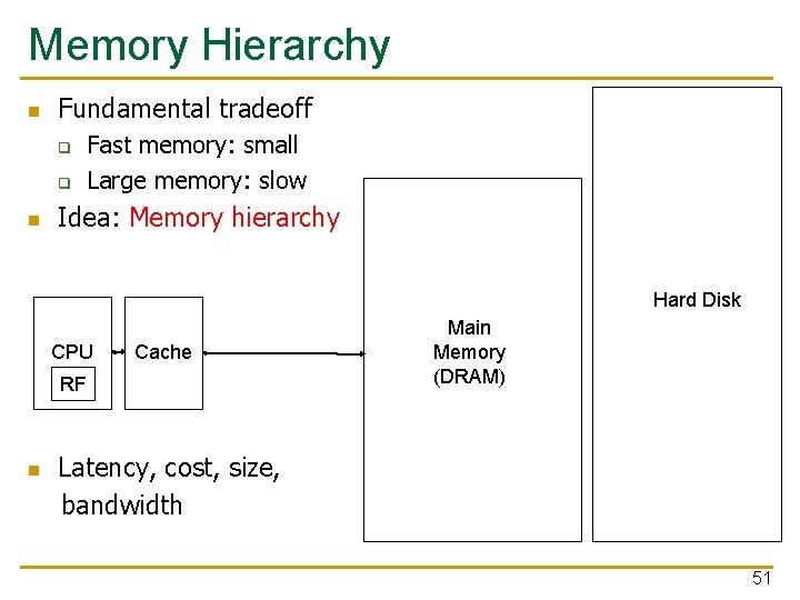
Memory Hierarchy n Fundamental tradeoff q q n Fast memory: small Large memory: slow Idea: Memory hierarchy Hard Disk CPU Cache RF n Main Memory (DRAM) Latency, cost, size, bandwidth 51

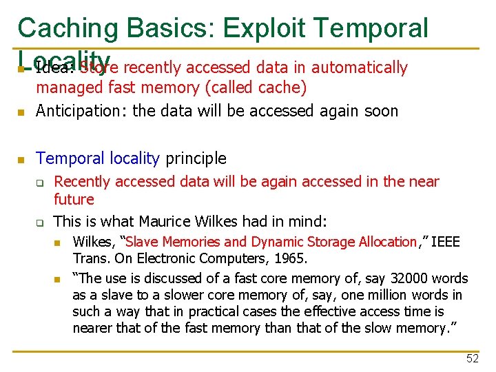
Caching Basics: Exploit Temporal Locality n Idea: Store recently accessed data in automatically n managed fast memory (called cache) Anticipation: the data will be accessed again soon n Temporal locality principle q q Recently accessed data will be again accessed in the near future This is what Maurice Wilkes had in mind: n n Wilkes, “Slave Memories and Dynamic Storage Allocation, ” IEEE Trans. On Electronic Computers, 1965. “The use is discussed of a fast core memory of, say 32000 words as a slave to a slower core memory of, say, one million words in such a way that in practical cases the effective access time is nearer that of the fast memory than that of the slow memory. ” 52

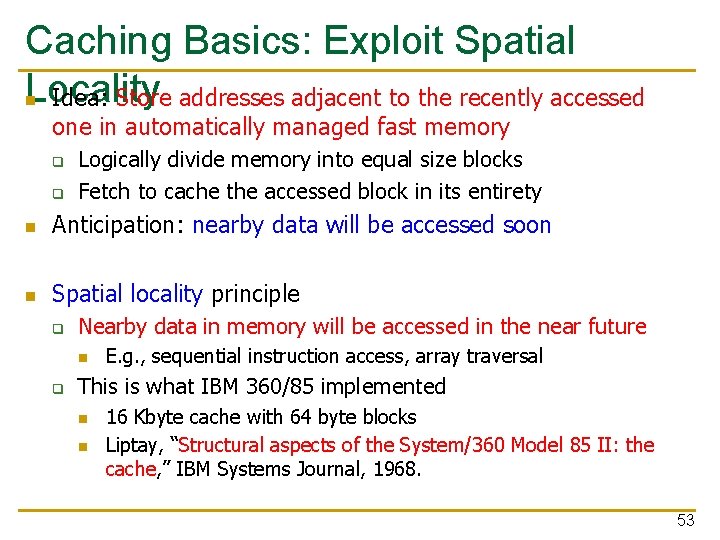
Caching Basics: Exploit Spatial Locality n Idea: Store addresses adjacent to the recently accessed one in automatically managed fast memory q q Logically divide memory into equal size blocks Fetch to cache the accessed block in its entirety n Anticipation: nearby data will be accessed soon n Spatial locality principle q Nearby data in memory will be accessed in the near future n q E. g. , sequential instruction access, array traversal This is what IBM 360/85 implemented n n 16 Kbyte cache with 64 byte blocks Liptay, “Structural aspects of the System/360 Model 85 II: the cache, ” IBM Systems Journal, 1968. 53

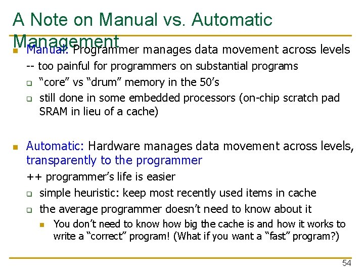
A Note on Manual vs. Automatic Management n Manual: Programmer manages data movement across levels -- too painful for programmers on substantial programs q “core” vs “drum” memory in the 50’s q still done in some embedded processors (on-chip scratch pad SRAM in lieu of a cache) n Automatic: Hardware manages data movement across levels, transparently to the programmer ++ programmer’s life is easier q simple heuristic: keep most recently used items in cache q the average programmer doesn’t need to know about it n You don’t need to know how big the cache is and how it works to write a “correct” program! (What if you want a “fast” program? ) 54

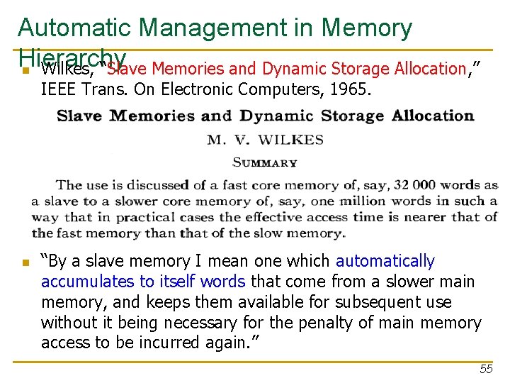
Automatic Management in Memory Hierarchy n Wilkes, “Slave Memories and Dynamic Storage Allocation, ” IEEE Trans. On Electronic Computers, 1965. n “By a slave memory I mean one which automatically accumulates to itself words that come from a slower main memory, and keeps them available for subsequent use without it being necessary for the penalty of main memory access to be incurred again. ” 55

A Modern Memory Hierarchy Register File 32 words, sub-nsec Memory Abstraction L 1 cache ~32 KB, ~nsec L 2 cache 512 KB ~ 1 MB, many nsec L 3 cache, . . . Main memory (DRAM), GB, ~100 nsec Swap Disk 100 GB, ~10 msec manual/compiler register spilling Automatic HW cache management automatic demand paging 56

The DRAM Subsystem

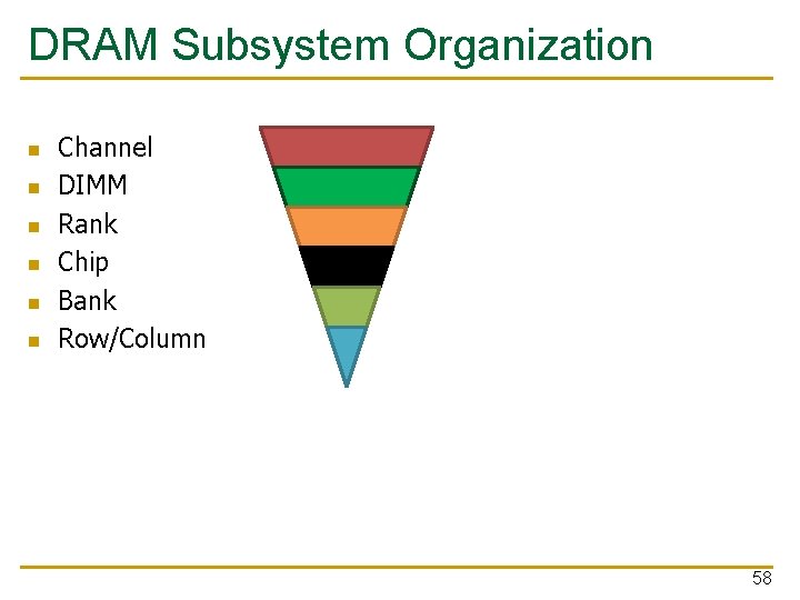
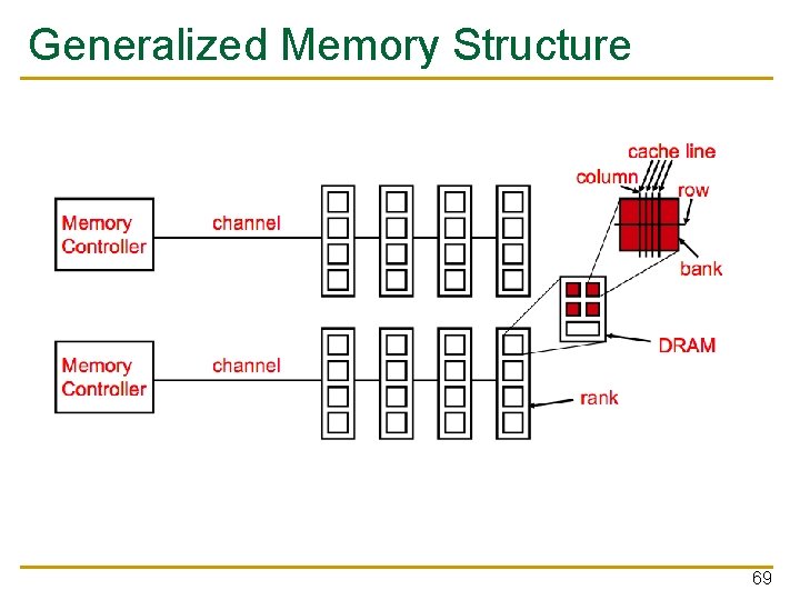
DRAM Subsystem Organization n n n Channel DIMM Rank Chip Bank Row/Column 58

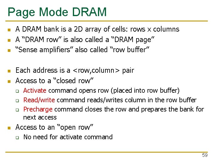
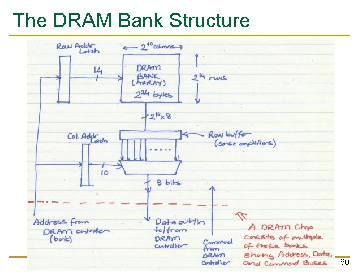
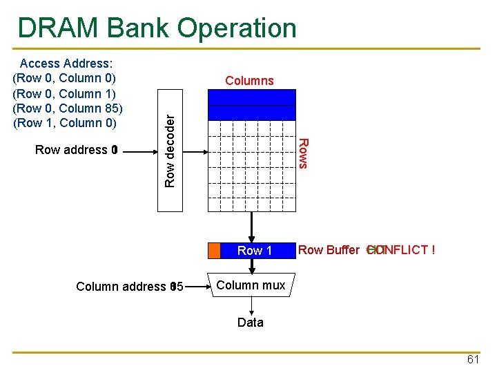
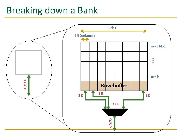
Page Mode DRAM n n n A DRAM bank is a 2 D array of cells: rows x columns A “DRAM row” is also called a “DRAM page” “Sense amplifiers” also called “row buffer” Each address is a <row, column> pair Access to a “closed row” q q q n Activate command opens row (placed into row buffer) Read/write command reads/writes column in the row buffer Precharge command closes the row and prepares the bank for next access Access to an “open row” q No need for activate command 59

The DRAM Bank Structure 60

DRAM Bank Operation Rows Row address 0 1 Columns Row decoder Access Address: (Row 0, Column 0) (Row 0, Column 1) (Row 0, Column 85) (Row 1, Column 0) Row 01 Row Empty Column address 0 1 85 Row Buffer CONFLICT HIT ! Column mux Data 61

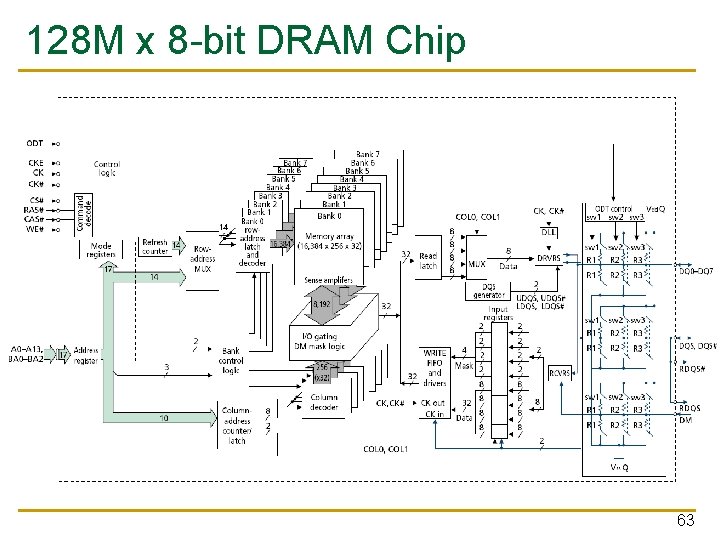
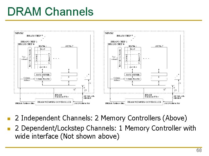
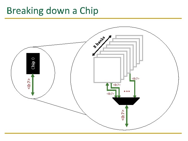
The DRAM Chip n n Consists of multiple banks (8 is a common number today) Banks share command/address/data buses The chip itself has a narrow interface (4 -16 bits per read) Changing the number of banks, size of the interface (pins), whether or not command/address/data buses are shared has significant impact on DRAM system cost 62

128 M x 8 -bit DRAM Chip 63

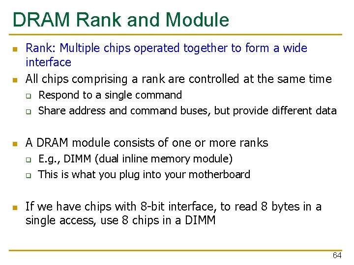
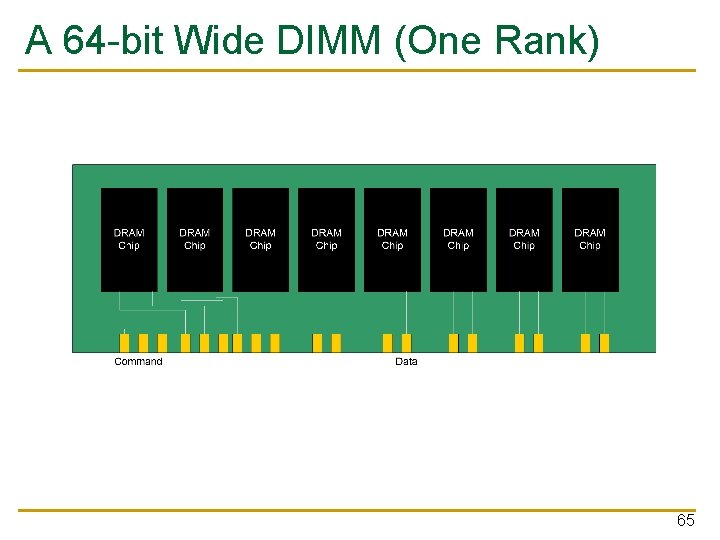
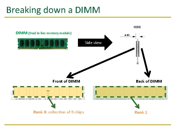
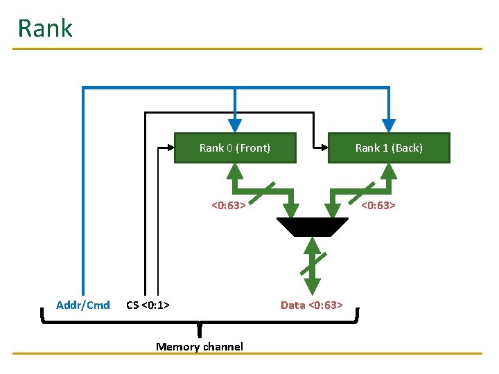
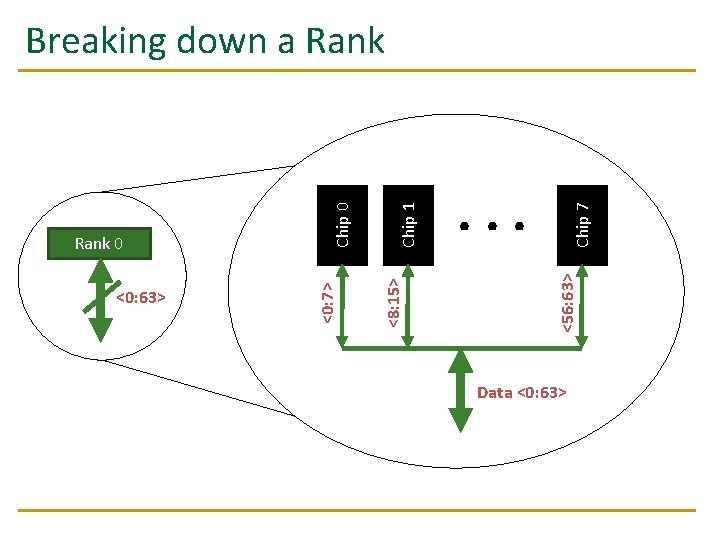
DRAM Rank and Module n n Rank: Multiple chips operated together to form a wide interface All chips comprising a rank are controlled at the same time q q n A DRAM module consists of one or more ranks q q n Respond to a single command Share address and command buses, but provide different data E. g. , DIMM (dual inline memory module) This is what you plug into your motherboard If we have chips with 8 -bit interface, to read 8 bytes in a single access, use 8 chips in a DIMM 64

A 64 -bit Wide DIMM (One Rank) 65

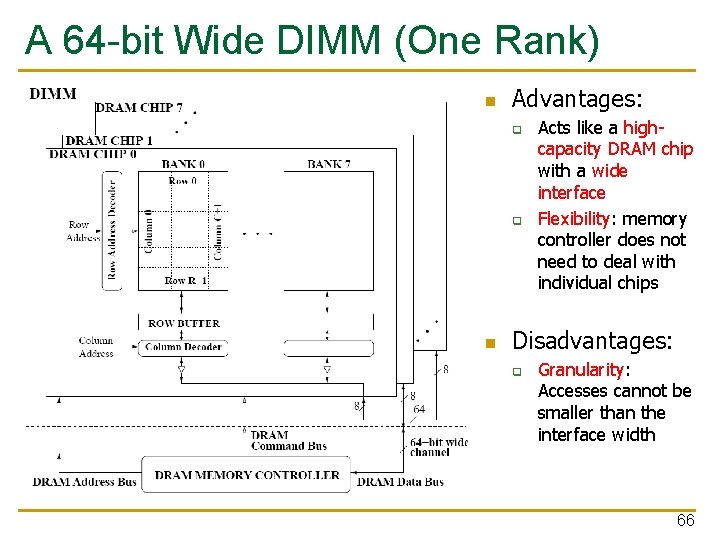
A 64 -bit Wide DIMM (One Rank) n Advantages: q q n Acts like a highcapacity DRAM chip with a wide interface Flexibility: memory controller does not need to deal with individual chips Disadvantages: q Granularity: Accesses cannot be smaller than the interface width 66

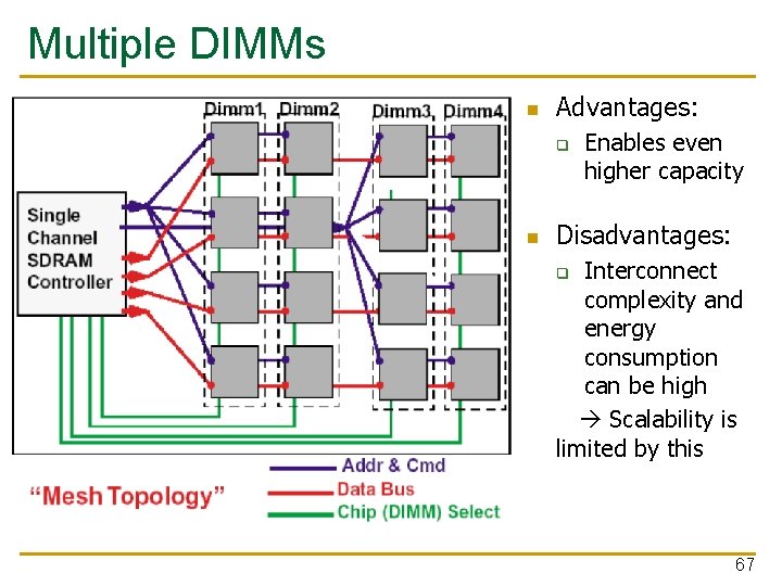
Multiple DIMMs n Advantages: q n Enables even higher capacity Disadvantages: Interconnect complexity and energy consumption can be high Scalability is limited by this q 67

DRAM Channels n n 2 Independent Channels: 2 Memory Controllers (Above) 2 Dependent/Lockstep Channels: 1 Memory Controller with wide interface (Not shown above) 68

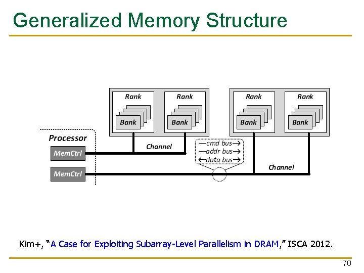
Generalized Memory Structure 69

Generalized Memory Structure Kim+, “A Case for Exploiting Subarray-Level Parallelism in DRAM, ” ISCA 2012. 70

The DRAM Subsystem The Top Down View

DRAM Subsystem Organization n n n Channel DIMM Rank Chip Bank Row/Column 72

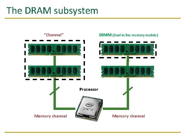
The DRAM subsystem “Channel” DIMM (Dual in-line memory module) Processor Memory channel

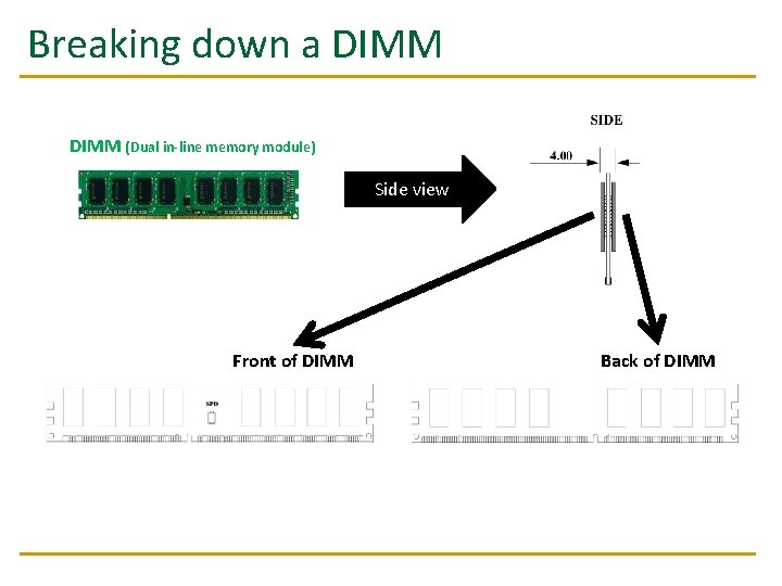
Breaking down a DIMM (Dual in-line memory module) Side view Front of DIMM Back of DIMM

Breaking down a DIMM (Dual in-line memory module) Side view Front of DIMM Rank 0: collection of 8 chips Back of DIMM Rank 1

Rank 0 (Front) Rank 1 (Back) <0: 63> Addr/Cmd CS <0: 1> Memory channel <0: 63> Data <0: 63>

Chip 7 . . . <56: 63> Chip 1 <8: 15> <0: 63> <0: 7> Rank 0 Chip 0 Breaking down a Rank Data <0: 63>

Bank 0 <0: 7> . . . <0: 7> Chip 0 8 b an ks Breaking down a Chip

Breaking down a Bank 2 k. B 1 B (column) row 16 k-1 . . . Bank 0 <0: 7> row 0 Row-buffer 1 B . . . <0: 7> 1 B 1 B

DRAM Subsystem Organization n n n Channel DIMM Rank Chip Bank Row/Column 80

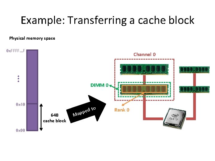
Example: Transferring a cache block Physical memory space 0 x. FFFF…F . . . Channel 0 DIMM 0 0 x 40 64 B cache block 0 x 00 to d e p Map Rank 0

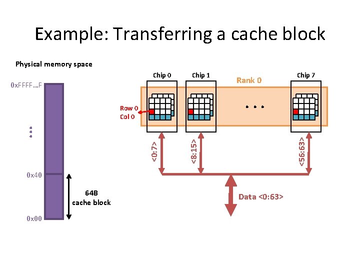
Example: Transferring a cache block Physical memory space Chip 0 Chip 1 0 x. FFFF…F Rank 0 Chip 7 <56: 63> <8: 15> <0: 7> . . . 0 x 40 64 B cache block 0 x 00 Data <0: 63>

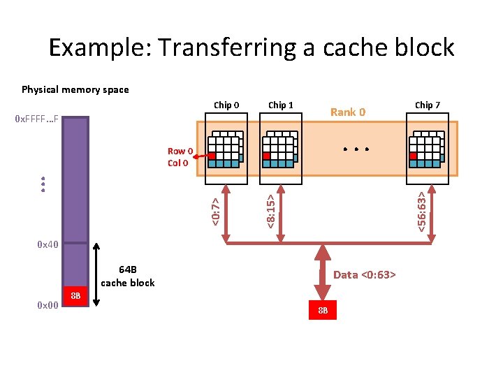
Example: Transferring a cache block Physical memory space Chip 0 Chip 1 0 x. FFFF…F Rank 0 . . . <56: 63> <8: 15> <0: 7> . . . Row 0 Col 0 0 x 40 64 B cache block 0 x 00 Chip 7 Data <0: 63>

Example: Transferring a cache block Physical memory space Chip 0 Chip 1 Rank 0 0 x. FFFF…F . . . <56: 63> <8: 15> <0: 7> . . . Row 0 Col 0 0 x 40 64 B cache block 0 x 00 Chip 7 Data <0: 63> 8 B 8 B

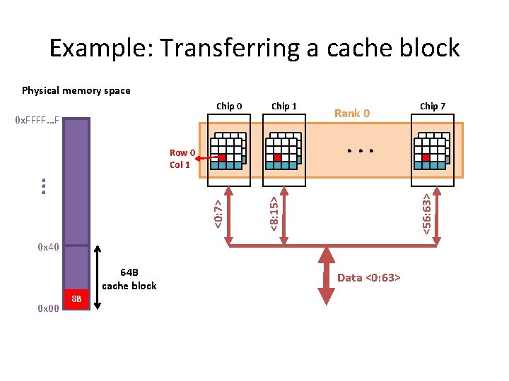
Example: Transferring a cache block Physical memory space Chip 0 Chip 1 0 x. FFFF…F Rank 0 . . . <56: 63> <8: 15> <0: 7> . . . Row 0 Col 1 0 x 40 64 B cache block 0 x 00 8 B Chip 7 Data <0: 63>

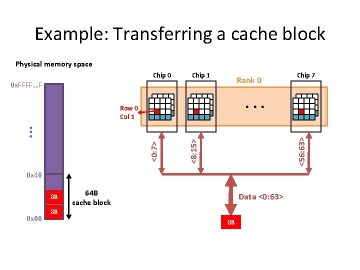
Example: Transferring a cache block Physical memory space Chip 0 Chip 1 Rank 0 0 x. FFFF…F . . . <56: 63> <8: 15> <0: 7> . . . Row 0 Col 1 0 x 40 8 B 0 x 00 Chip 7 64 B cache block Data <0: 63> 8 B 8 B

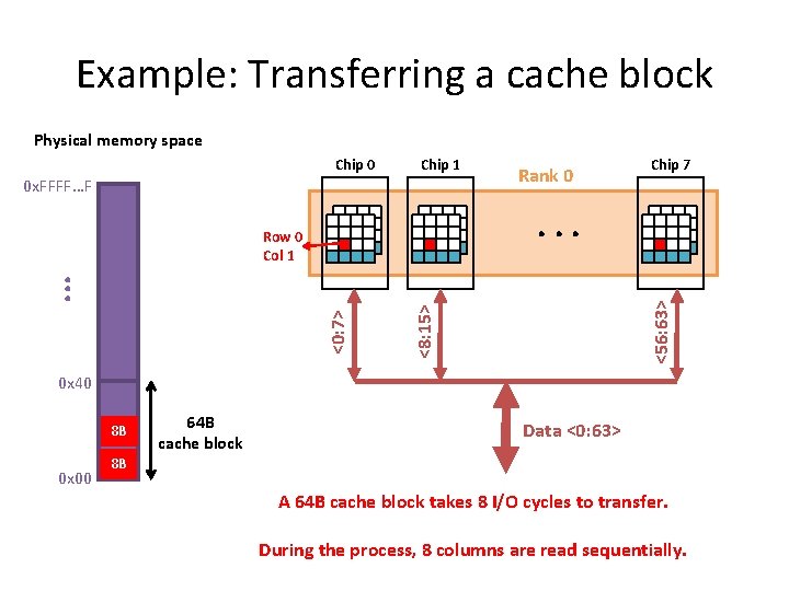
Example: Transferring a cache block Physical memory space Chip 0 Chip 1 0 x. FFFF…F Rank 0 Chip 7 . . . <56: 63> <8: 15> <0: 7> . . . Row 0 Col 1 0 x 40 8 B 0 x 00 64 B cache block Data <0: 63> 8 B A 64 B cache block takes 8 I/O cycles to transfer. During the process, 8 columns are read sequentially.

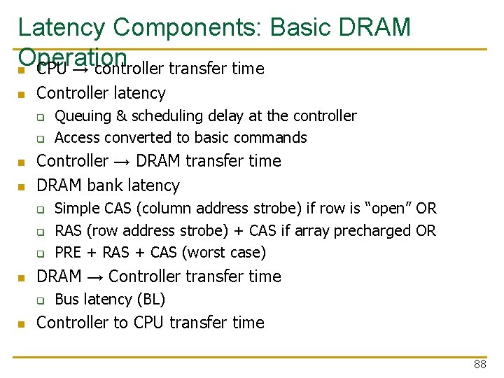
Latency Components: Basic DRAM Operation n CPU → controller transfer time n Controller latency q q n n Controller → DRAM transfer time DRAM bank latency q q q n Simple CAS (column address strobe) if row is “open” OR RAS (row address strobe) + CAS if array precharged OR PRE + RAS + CAS (worst case) DRAM → Controller transfer time q n Queuing & scheduling delay at the controller Access converted to basic commands Bus latency (BL) Controller to CPU transfer time 88

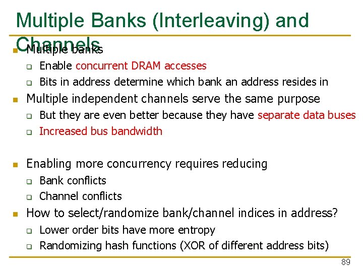
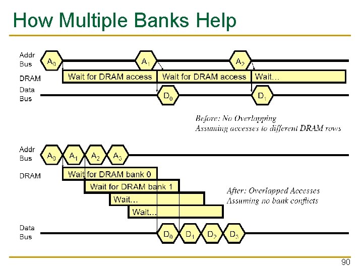
Multiple Banks (Interleaving) and n. Channels Multiple banks q q n Multiple independent channels serve the same purpose q q n But they are even better because they have separate data buses Increased bus bandwidth Enabling more concurrency requires reducing q q n Enable concurrent DRAM accesses Bits in address determine which bank an address resides in Bank conflicts Channel conflicts How to select/randomize bank/channel indices in address? q q Lower order bits have more entropy Randomizing hash functions (XOR of different address bits) 89

How Multiple Banks Help 90

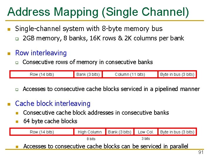
Address Mapping (Single Channel) n Single-channel system with 8 -byte memory bus q n 2 GB memory, 8 banks, 16 K rows & 2 K columns per bank Row interleaving q Consecutive rows of memory in consecutive banks Row (14 bits) q n Bank (3 bits) Column (11 bits) Byte in bus (3 bits) Accesses to consecutive cache blocks serviced in a pipelined manner Cache block interleaving n n Consecutive cache block addresses in consecutive banks 64 byte cache blocks Row (14 bits) High Column 8 bits n Bank (3 bits) Low Col. Byte in bus (3 bits) 3 bits Accesses to consecutive cache blocks can be serviced in parallel 91

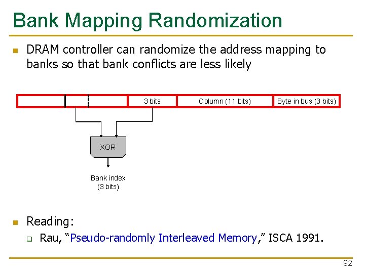
Bank Mapping Randomization n DRAM controller can randomize the address mapping to banks so that bank conflicts are less likely 3 bits Column (11 bits) Byte in bus (3 bits) XOR Bank index (3 bits) n Reading: q Rau, “Pseudo-randomly Interleaved Memory, ” ISCA 1991. 92

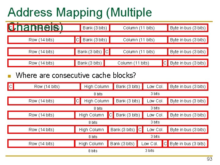
Address Mapping (Multiple Channels) C Row (14 bits) n C Bank (3 bits) Column (11 bits) Byte in bus (3 bits) Row (14 bits) Bank (3 bits) Column (11 bits) C Byte in bus (3 bits) Where are consecutive cache blocks? Row (14 bits) High Column Bank (3 bits) Low Col. 3 bits 8 bits Row (14 bits) C High Column Bank (3 bits) Low Col. High Column C Bank (3 bits) Low Col. High Column Bank (3 bits) C High Column 8 bits Low Col. Byte in bus (3 bits) 3 bits 8 bits Row (14 bits) Byte in bus (3 bits) Bank (3 bits) Low Col. C Byte in bus (3 bits) 3 bits 93

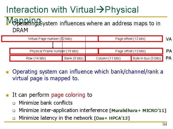
Interaction with Virtual Physical Mapping n Operating System influences where an address maps to in DRAM Virtual Page number (52 bits) Physical Frame number (19 bits) Row (14 bits) n n Bank (3 bits) Page offset (12 bits) VA Page offset (12 bits) PA Column (11 bits) PA Byte in bus (3 bits) Operating system can influence which bank/channel/rank a virtual page is mapped to. It can perform page coloring to q q q Minimize bank conflicts Minimize inter-application interference [Muralidhara+ MICRO’ 11] Minimize latency in the network [Das+ HPCA’ 13] 94

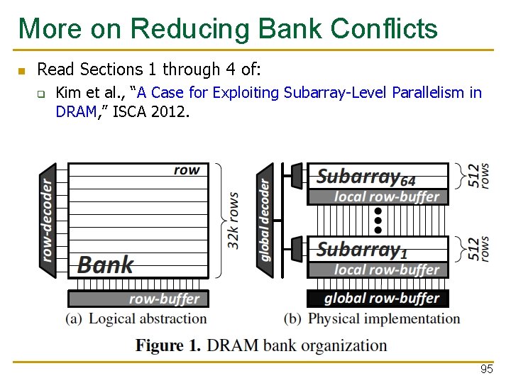
More on Reducing Bank Conflicts n Read Sections 1 through 4 of: q Kim et al. , “A Case for Exploiting Subarray-Level Parallelism in DRAM, ” ISCA 2012. 95

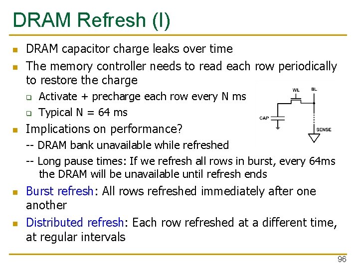
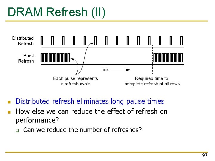
DRAM Refresh (I) n n DRAM capacitor charge leaks over time The memory controller needs to read each row periodically to restore the charge q q n Activate + precharge each row every N ms Typical N = 64 ms Implications on performance? -- DRAM bank unavailable while refreshed -- Long pause times: If we refresh all rows in burst, every 64 ms the DRAM will be unavailable until refresh ends n n Burst refresh: All rows refreshed immediately after one another Distributed refresh: Each row refreshed at a different time, at regular intervals 96

DRAM Refresh (II) n n Distributed refresh eliminates long pause times How else we can reduce the effect of refresh on performance? q Can we reduce the number of refreshes? 97

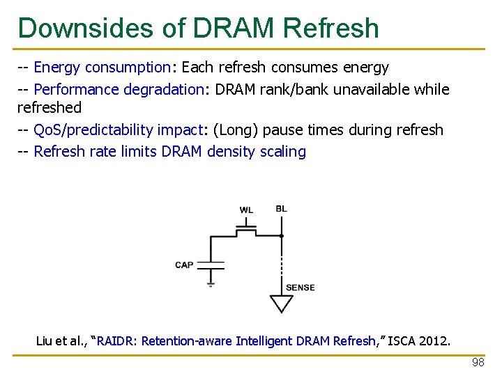
Downsides of DRAM Refresh -- Energy consumption: Each refresh consumes energy -- Performance degradation: DRAM rank/bank unavailable while refreshed -- Qo. S/predictability impact: (Long) pause times during refresh -- Refresh rate limits DRAM density scaling Liu et al. , “RAIDR: Retention-aware Intelligent DRAM Refresh, ” ISCA 2012. 98

Memory Controllers

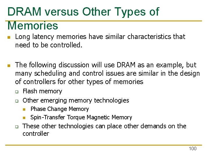
DRAM versus Other Types of Memories n n Long latency memories have similar characteristics that need to be controlled. The following discussion will use DRAM as an example, but many scheduling and control issues are similar in the design of controllers for other types of memories q q Flash memory Other emerging memory technologies n n q Phase Change Memory Spin-Transfer Torque Magnetic Memory These other technologies can place other demands on the controller 100

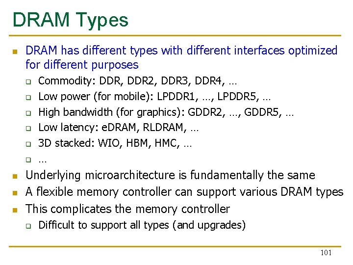
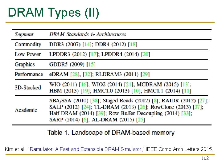
DRAM Types n DRAM has different types with different interfaces optimized for different purposes q q q n n n Commodity: DDR, DDR 2, DDR 3, DDR 4, … Low power (for mobile): LPDDR 1, …, LPDDR 5, … High bandwidth (for graphics): GDDR 2, …, GDDR 5, … Low latency: e. DRAM, RLDRAM, … 3 D stacked: WIO, HBM, HMC, … … Underlying microarchitecture is fundamentally the same A flexible memory controller can support various DRAM types This complicates the memory controller q Difficult to support all types (and upgrades) 101

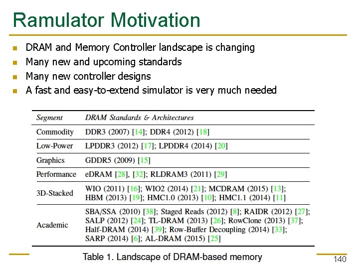
DRAM Types (II) Kim et al. , “Ramulator: A Fast and Extensible DRAM Simulator, ” IEEE Comp Arch Letters 2015. 102

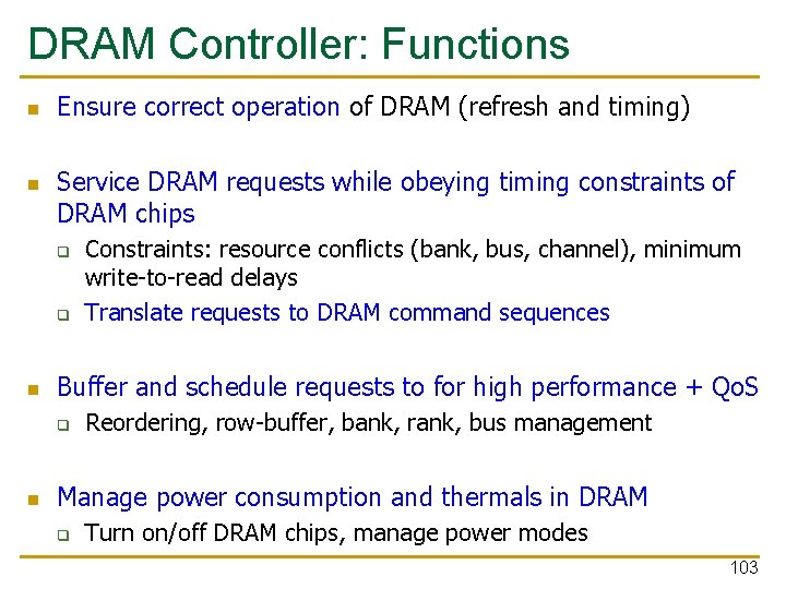
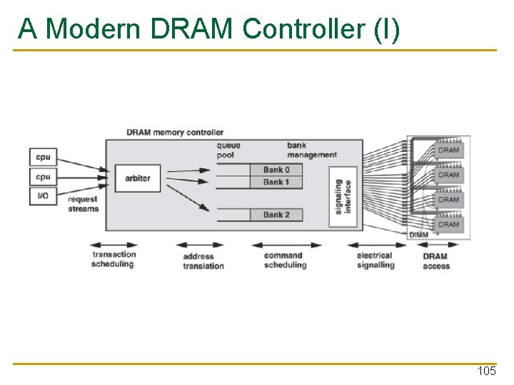
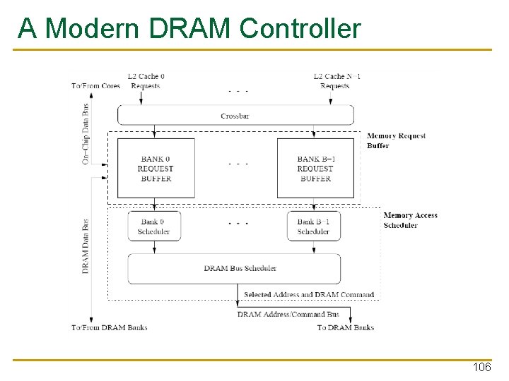
DRAM Controller: Functions n n Ensure correct operation of DRAM (refresh and timing) Service DRAM requests while obeying timing constraints of DRAM chips q q n Buffer and schedule requests to for high performance + Qo. S q n Constraints: resource conflicts (bank, bus, channel), minimum write-to-read delays Translate requests to DRAM command sequences Reordering, row-buffer, bank, rank, bus management Manage power consumption and thermals in DRAM q Turn on/off DRAM chips, manage power modes 103

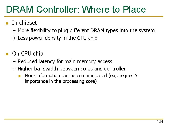
DRAM Controller: Where to Place n In chipset + More flexibility to plug different DRAM types into the system + Less power density in the CPU chip n On CPU chip + Reduced latency for main memory access + Higher bandwidth between cores and controller n More information can be communicated (e. g. request’s importance in the processing core) 104

A Modern DRAM Controller (I) 105

A Modern DRAM Controller 106

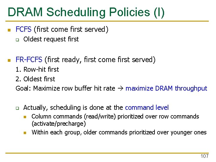
DRAM Scheduling Policies (I) n FCFS (first come first served) q n Oldest request first FR-FCFS (first ready, first come first served) 1. Row-hit first 2. Oldest first Goal: Maximize row buffer hit rate maximize DRAM throughput q Actually, scheduling is done at the command level n n Column commands (read/write) prioritized over row commands (activate/precharge) Within each group, older commands prioritized over younger ones 107

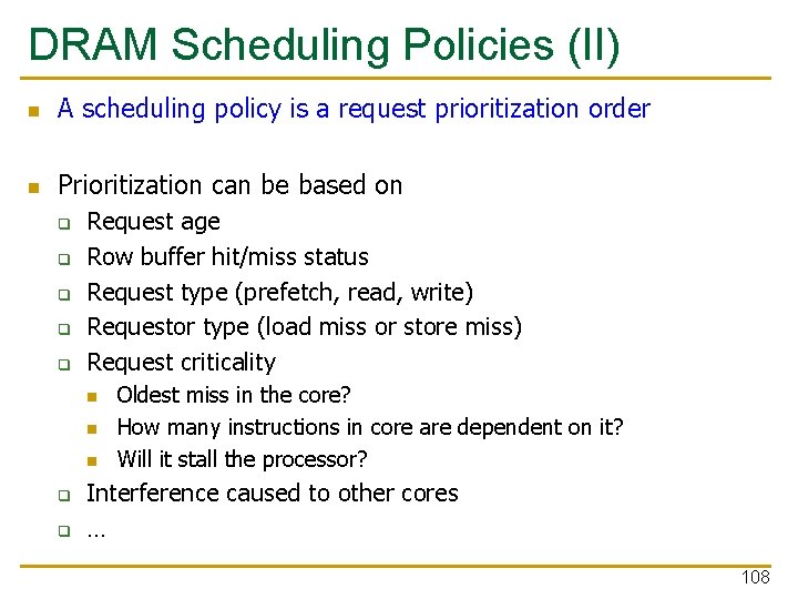
DRAM Scheduling Policies (II) n A scheduling policy is a request prioritization order n Prioritization can be based on q q q Request age Row buffer hit/miss status Request type (prefetch, read, write) Requestor type (load miss or store miss) Request criticality n n n q q Oldest miss in the core? How many instructions in core are dependent on it? Will it stall the processor? Interference caused to other cores … 108

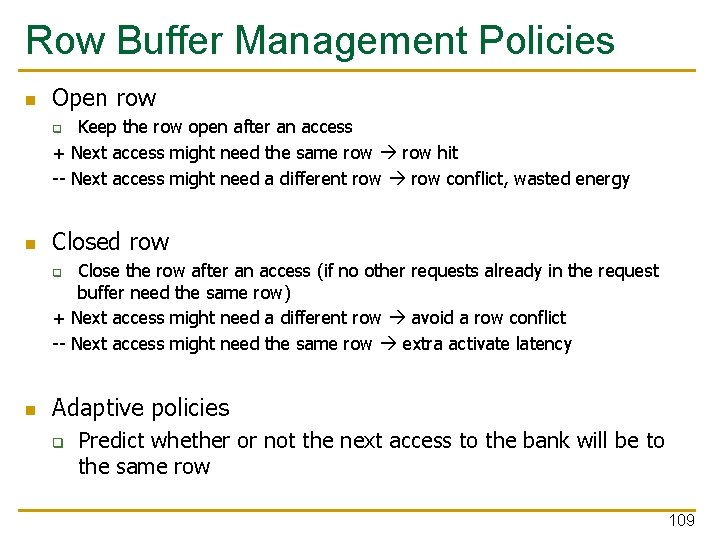
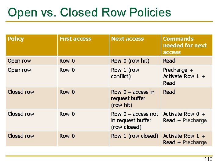
Row Buffer Management Policies n Open row Keep the row open after an access + Next access might need the same row hit -- Next access might need a different row conflict, wasted energy q n Closed row Close the row after an access (if no other requests already in the request buffer need the same row) + Next access might need a different row avoid a row conflict -- Next access might need the same row extra activate latency q n Adaptive policies q Predict whether or not the next access to the bank will be to the same row 109

Open vs. Closed Row Policies Policy First access Next access Commands needed for next access Open row Row 0 (row hit) Read Open row Row 0 Row 1 (row conflict) Precharge + Activate Row 1 + Read Closed row Row 0 – access in request buffer (row hit) Read Closed row Row 0 – access not Activate Row 0 + in request buffer Read + Precharge (row closed) Closed row Row 0 Row 1 (row closed) Activate Row 1 + Read + Precharge 110

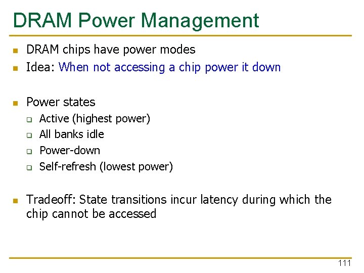
DRAM Power Management n DRAM chips have power modes Idea: When not accessing a chip power it down n Power states n q q n Active (highest power) All banks idle Power-down Self-refresh (lowest power) Tradeoff: State transitions incur latency during which the chip cannot be accessed 111

Difficulty of DRAM Control

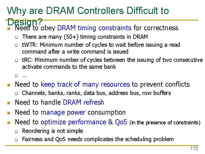
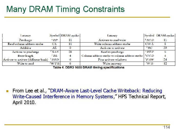
Why are DRAM Controllers Difficult to Design? n Need to obey DRAM timing constraints for correctness q q n Need to keep track of many resources to prevent conflicts q n n n There are many (50+) timing constraints in DRAM t. WTR: Minimum number of cycles to wait before issuing a read command after a write command is issued t. RC: Minimum number of cycles between the issuing of two consecutive activate commands to the same bank … Channels, banks, ranks, data bus, address bus, row buffers Need to handle DRAM refresh Need to manage power consumption Need to optimize performance & Qo. S q q (in the presence of constraints) Reordering is not simple Fairness and Qo. S needs complicates the scheduling problem 113

Many DRAM Timing Constraints n From Lee et al. , “DRAM-Aware Last-Level Cache Writeback: Reducing Write-Caused Interference in Memory Systems, ” HPS Technical Report, April 2010. 114

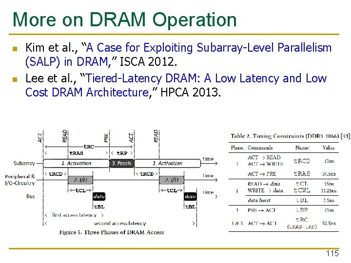
More on DRAM Operation n n Kim et al. , “A Case for Exploiting Subarray-Level Parallelism (SALP) in DRAM, ” ISCA 2012. Lee et al. , “Tiered-Latency DRAM: A Low Latency and Low Cost DRAM Architecture, ” HPCA 2013. 115

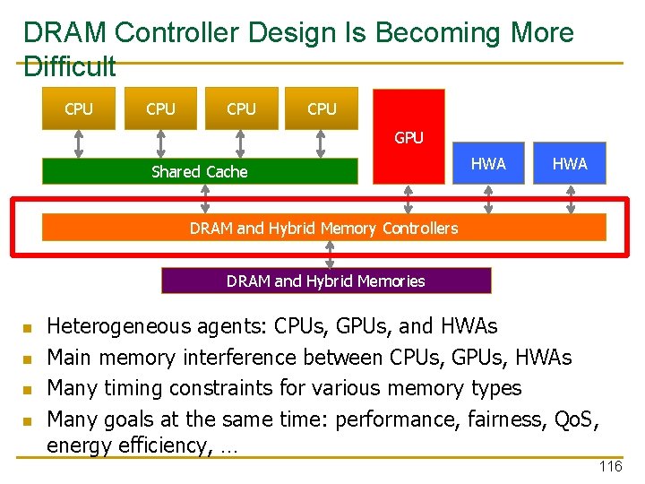
DRAM Controller Design Is Becoming More Difficult CPU CPU GPU Shared Cache HWA DRAM and Hybrid Memory Controllers DRAM and Hybrid Memories n n Heterogeneous agents: CPUs, GPUs, and HWAs Main memory interference between CPUs, GPUs, HWAs Many timing constraints for various memory types Many goals at the same time: performance, fairness, Qo. S, energy efficiency, … 116

Reality and Dream n n Reality: It difficult to optimize all these different constraints while maximizing performance, Qo. S, energy-efficiency, … Dream: Wouldn’t it be nice if the DRAM controller automatically found a good scheduling policy on its own? 117

Self-Optimizing DRAM Controllers n n Problem: DRAM controllers difficult to design It is difficult for human designers to design a policy that can adapt itself very well to different workloads and different system conditions Idea: Design a memory controller that adapts its scheduling policy decisions to workload behavior and system conditions using machine learning. Observation: Reinforcement learning maps nicely to memory control. Design: Memory controller is a reinforcement learning agent that dynamically and continuously learns and employs the best scheduling policy. 118 Ipek+, “Self Optimizing Memory Controllers: A Reinforcement Learning Approach, ” ISCA 2008.

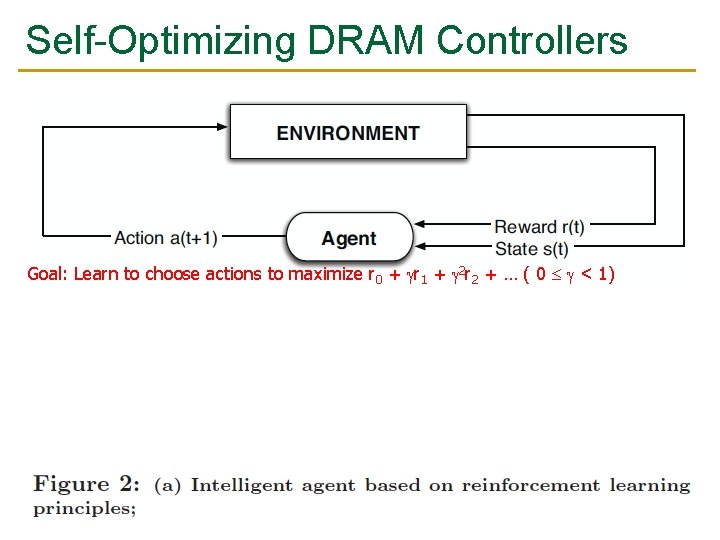
Self-Optimizing DRAM Controllers n Engin Ipek, Onur Mutlu, José F. Martínez, and Rich Caruana, "Self Optimizing Memory Controllers: A Reinforcement Learning Approach" Proceedings of the 35 th International Symposium on Computer Architecture (ISCA), pages 39 -50, Beijing, China, June 2008. Goal: Learn to choose actions to maximize r 0 + r 1 + 2 r 2 + … ( 0 < 1) 119

Next Lecture (9/30): Required Readings Ø Required Reading Assignment: • Lee et al. , “Phase Change Technology and the Future of Main Memory, ” IEEE Micro, Jan/Feb 2010. Ø Recommended References: • M. Qureshi et al. , “Scalable high performance main memory system using phase-change memory technology, ” ISCA 2009. • H. Yoon et al. , “Row buffer locality aware caching policies for hybrid memories, ” ICCD 2012. • J. Zhao et al. , “FIRM: Fair and High-Performance Memory Control for Persistent Memory Systems, ” MICRO 2014. 120

18 -740/640 Computer Architecture Lecture 8: Main Memory System Prof. Onur Mutlu Carnegie Mellon University Fall 2015, 9/28/2015

We did not cover the remaining slides in lecture. They are for your benefit.

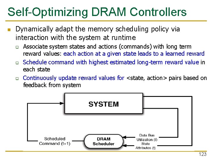
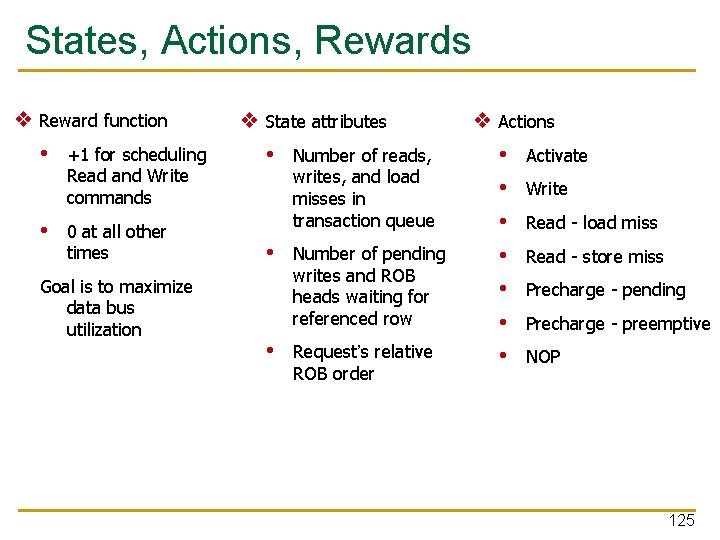
Self-Optimizing DRAM Controllers n Dynamically adapt the memory scheduling policy via interaction with the system at runtime q q q Associate system states and actions (commands) with long term reward values: each action at a given state leads to a learned reward Schedule command with highest estimated long-term reward value in each state Continuously update reward values for <state, action> pairs based on feedback from system 123

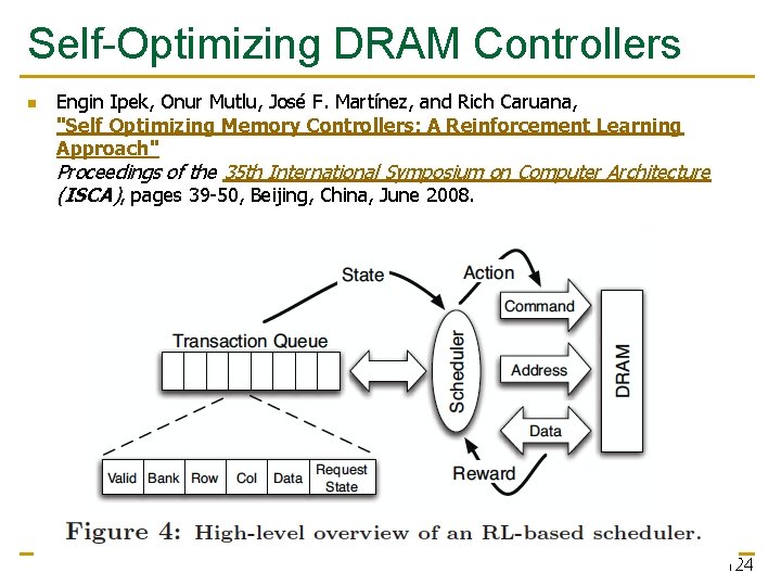
Self-Optimizing DRAM Controllers n Engin Ipek, Onur Mutlu, José F. Martínez, and Rich Caruana, "Self Optimizing Memory Controllers: A Reinforcement Learning Approach" Proceedings of the 35 th International Symposium on Computer Architecture (ISCA), pages 39 -50, Beijing, China, June 2008. 124

States, Actions, Rewards ❖ Reward function • +1 for scheduling Read and Write commands • 0 at all other times Goal is to maximize data bus utilization ❖ State attributes • Number of reads, writes, and load misses in transaction queue • Number of pending writes and ROB heads waiting for referenced row • Request’s relative ROB order ❖ Actions • Activate • Write • Read - load miss • Read - store miss • Precharge - pending • Precharge - preemptive • NOP 125

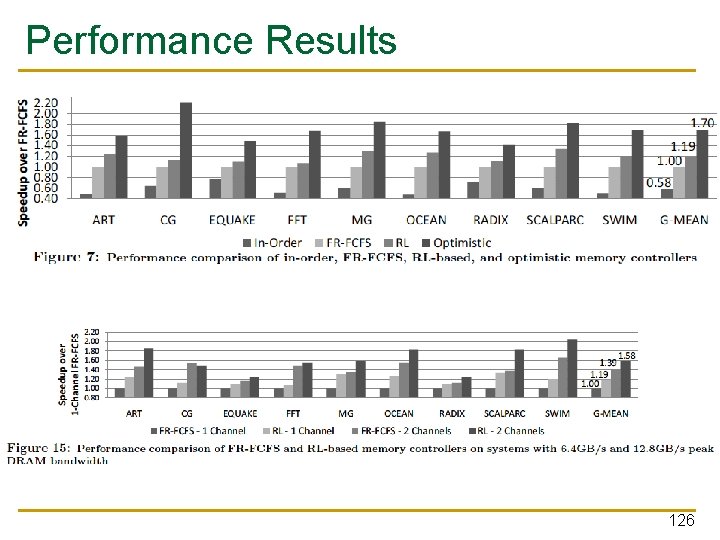
Performance Results 126

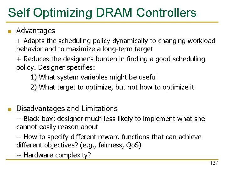
Self Optimizing DRAM Controllers n Advantages + Adapts the scheduling policy dynamically to changing workload behavior and to maximize a long-term target + Reduces the designer’s burden in finding a good scheduling policy. Designer specifies: 1) What system variables might be useful 2) What target to optimize, but not how to optimize it n Disadvantages and Limitations -- Black box: designer much less likely to implement what she cannot easily reason about -- How to specify different reward functions that can achieve different objectives? (e. g. , fairness, Qo. S) -- Hardware complexity? 127

More on Self-Optimizing DRAM Controllers Engin Ipek, Onur Mutlu, José F. Martínez, and Rich Caruana, n "Self Optimizing Memory Controllers: A Reinforcement Learning Approach" Proceedings of the 35 th International Symposium on Computer Architecture (ISCA), pages 39 -50, Beijing, China, June 2008. 128

Evaluating New Ideas for New (Memory) Architectures

Simulation: The Field of Dreams

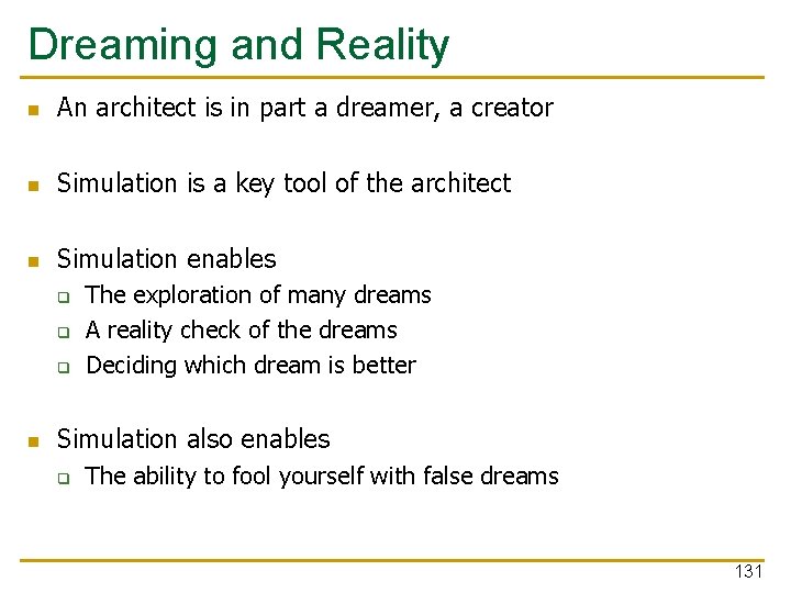
Dreaming and Reality n An architect is in part a dreamer, a creator n Simulation is a key tool of the architect n Simulation enables q q q n The exploration of many dreams A reality check of the dreams Deciding which dream is better Simulation also enables q The ability to fool yourself with false dreams 131

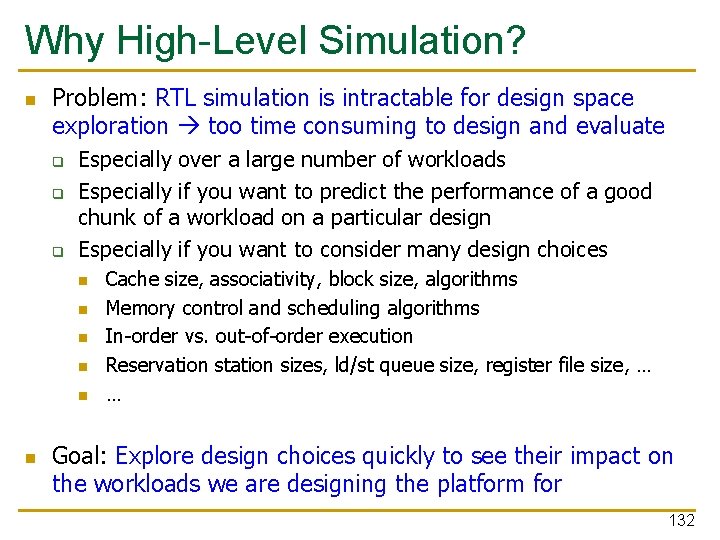
Why High-Level Simulation? n Problem: RTL simulation is intractable for design space exploration too time consuming to design and evaluate q q q Especially over a large number of workloads Especially if you want to predict the performance of a good chunk of a workload on a particular design Especially if you want to consider many design choices n n n Cache size, associativity, block size, algorithms Memory control and scheduling algorithms In-order vs. out-of-order execution Reservation station sizes, ld/st queue size, register file size, … … Goal: Explore design choices quickly to see their impact on the workloads we are designing the platform for 132

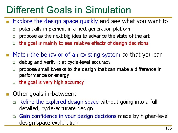
Different Goals in Simulation n Explore the design space quickly and see what you want to q q q n Match the behavior of an existing system so that you can q q q n potentially implement in a next-generation platform propose as the next big idea to advance the state of the art the goal is mainly to see relative effects of design decisions debug and verify it at cycle-level accuracy propose small tweaks to the design that can make a difference in performance or energy the goal is very high accuracy Other goals in-between: q q Refine the explored design space without going into a full detailed, cycle-accurate design Gain confidence in your design decisions made by higher-level design space exploration 133

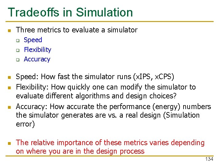
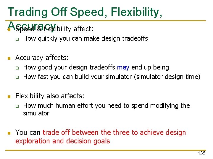
Tradeoffs in Simulation n Three metrics to evaluate a simulator q q q n n Speed Flexibility Accuracy Speed: How fast the simulator runs (x. IPS, x. CPS) Flexibility: How quickly one can modify the simulator to evaluate different algorithms and design choices? Accuracy: How accurate the performance (energy) numbers the simulator generates are vs. a real design (Simulation error) The relative importance of these metrics varies depending on where you are in the design process 134

Trading Off Speed, Flexibility, Accuracy n Speed & flexibility affect: q n Accuracy affects: q q n How good your design tradeoffs may end up being How fast you can build your simulator (simulator design time) Flexibility also affects: q n How quickly you can make design tradeoffs How much human effort you need to spend modifying the simulator You can trade off between the three to achieve design exploration and decision goals 135

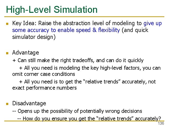
High-Level Simulation n n Key Idea: Raise the abstraction level of modeling to give up some accuracy to enable speed & flexibility (and quick simulator design) Advantage + Can still make the right tradeoffs, and can do it quickly + All you need is modeling the key high-level factors, you can omit corner case conditions + All you need is to get the “relative trends” accurately, not exact performance numbers n Disadvantage -- Opens up the possibility of potentially wrong decisions -- How do you ensure you get the “relative trends” accurately? 136

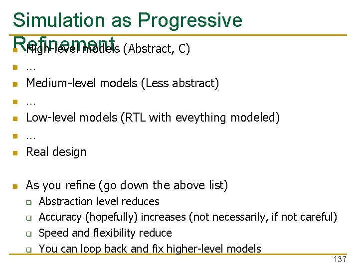
Simulation as Progressive Refinement n High-level models (Abstract, C) n … Medium-level models (Less abstract) … Low-level models (RTL with eveything modeled) … Real design n As you refine (go down the above list) n n n q q Abstraction level reduces Accuracy (hopefully) increases (not necessarily, if not careful) Speed and flexibility reduce You can loop back and fix higher-level models 137

Making The Best of Architecture n A good architect is comfortable at all levels of refinement q n Including the extremes A good architect knows when to use what type of simulation 138
![Ramulator A Fast and Extensible DRAM Simulator IEEE Comp Arch Letters 15 139 Ramulator: A Fast and Extensible DRAM Simulator [IEEE Comp Arch Letters’ 15] 139](https://slidetodoc.com/presentation_image_h2/d08edf6df9695906ae93866a8e50ef25/image-139.jpg)
Ramulator: A Fast and Extensible DRAM Simulator [IEEE Comp Arch Letters’ 15] 139

Ramulator Motivation n n DRAM and Memory Controller landscape is changing Many new and upcoming standards Many new controller designs A fast and easy-to-extend simulator is very much needed 140

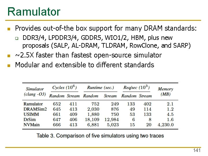
Ramulator n Provides out-of-the box support for many DRAM standards: q n n DDR 3/4, LPDDR 3/4, GDDR 5, WIO 1/2, HBM, plus new proposals (SALP, AL-DRAM, TLDRAM, Row. Clone, and SARP) ~2. 5 X faster than fastest open-source simulator Modular and extensible to different standards 141

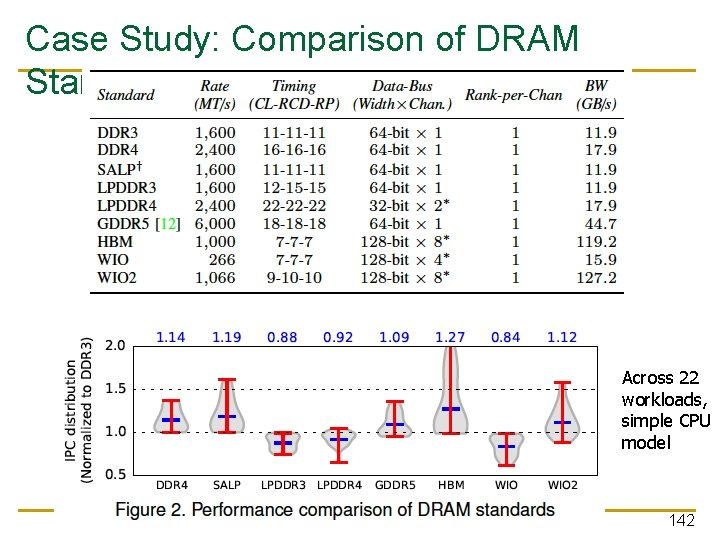
Case Study: Comparison of DRAM Standards Across 22 workloads, simple CPU model 142

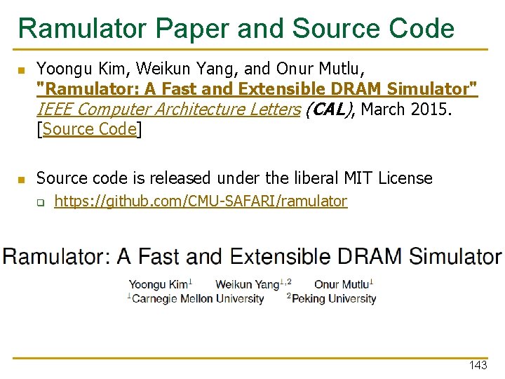
Ramulator Paper and Source Code n n Yoongu Kim, Weikun Yang, and Onur Mutlu, "Ramulator: A Fast and Extensible DRAM Simulator" IEEE Computer Architecture Letters (CAL), March 2015. [Source Code] Source code is released under the liberal MIT License q https: //github. com/CMU-SAFARI/ramulator 143

Extra Credit Assignment n Review the Ramulator paper q n Send your reviews to me (omutlu@gmail. com) Download and run Ramulator q q Compare DDR 3, DDR 4, SALP, HBM for the libquantum benchmark (provided in Ramulator repository) Send your brief report to me 144