Constructive Computer Architecture Tutorial 8 FPGA Synthesis Andy









- Slides: 43
Constructive Computer Architecture Tutorial 8: FPGA Synthesis Andy Wright 6. S 195 TA November 8, 2013 http: //csg. csail. mit. edu/6. s 195 T 08 -1
Lab Update FPGAs are working again n November 8, 2013 If you have any problems with them, let me know http: //csg. csail. mit. edu/6. s 195 T 08 -2
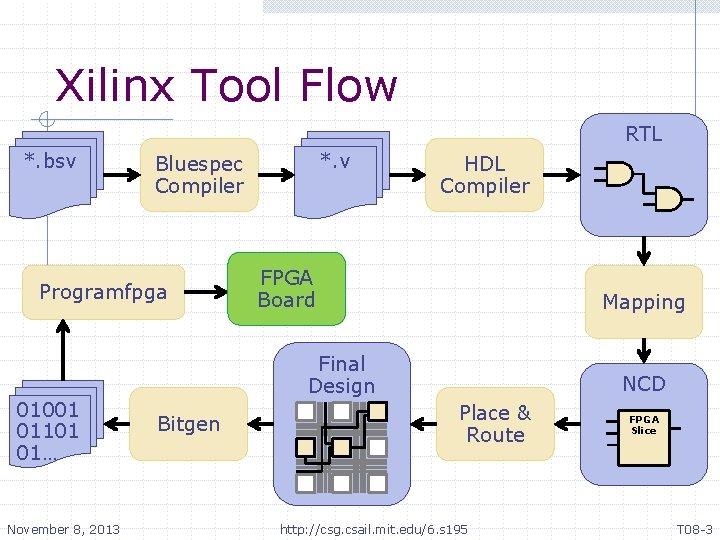
Xilinx Tool Flow RTL *. bsv Programfpga 01001 01101 01… November 8, 2013 *. v Bluespec Compiler HDL Compiler FPGA Board Mapping Final Design Bitgen NCD Place & Route http: //csg. csail. mit. edu/6. s 195 FPGA Slice T 08 -3
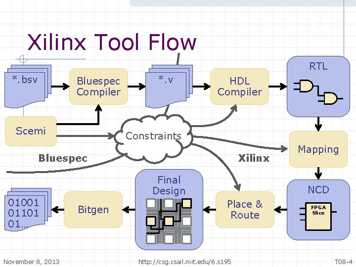
Xilinx Tool Flow RTL *. bsv Bluespec Compiler Scemi *. v HDL Compiler Constraints Bluespec 01001 01101 01… November 8, 2013 Xilinx Final Design Bitgen Mapping NCD Place & Route http: //csg. csail. mit. edu/6. s 195 FPGA Slice T 08 -4
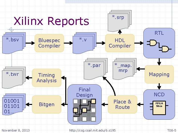
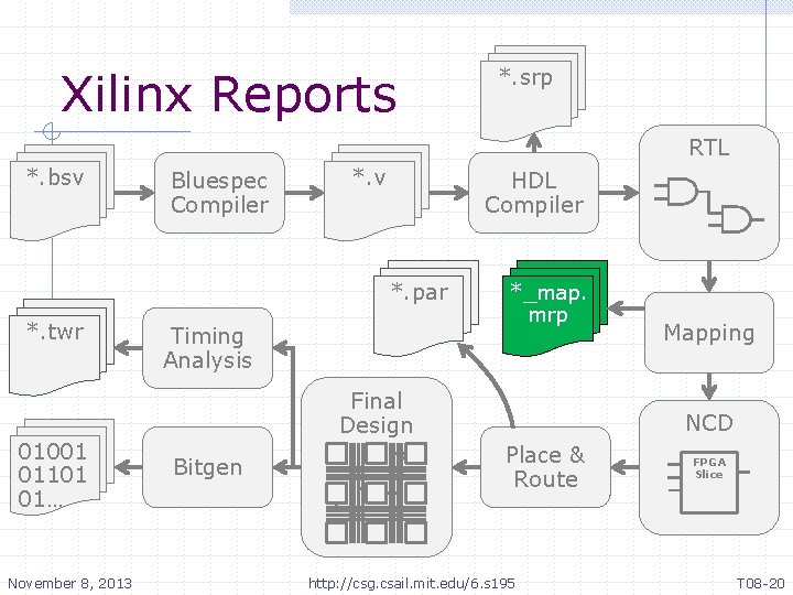
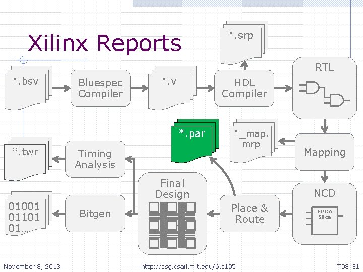
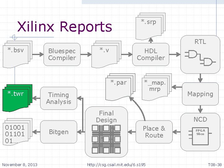
Xilinx Reports *. srp RTL *. bsv Bluespec Compiler *. v HDL Compiler *. par *. twr 01001 01101 01… November 8, 2013 *_map. mrp Timing Analysis Final Design Bitgen Mapping NCD Place & Route http: //csg. csail. mit. edu/6. s 195 FPGA Slice T 08 -5
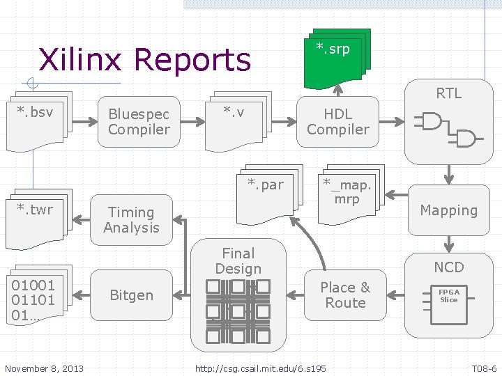
Xilinx Reports *. srp RTL *. bsv Bluespec Compiler *. v HDL Compiler *. par *. twr 01001 01101 01… November 8, 2013 *_map. mrp Timing Analysis Final Design Bitgen Mapping NCD Place & Route http: //csg. csail. mit. edu/6. s 195 FPGA Slice T 08 -6
mk. Bridge. srp Search for: “Low Level Synthesis” n n November 8, 2013 You’ll see some optimizations performed such as removing constant value registers. This portion removes unwanted overhead of EHRs http: //csg. csail. mit. edu/6. s 195 T 08 -7
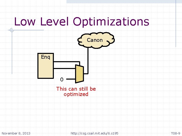
Low Level Optimizations Assume this fires every cycle Canon Enq 0 1 Register always 0 0 November 8, 2013 http: //csg. csail. mit. edu/6. s 195 0 T 08 -8
Low Level Optimizations Canon Enq 0 This can still be optimized November 8, 2013 http: //csg. csail. mit. edu/6. s 195 T 08 -9
Low Level Optimizations Canon Enq No overhead from using an EHR November 8, 2013 http: //csg. csail. mit. edu/6. s 195 T 08 -10
mk. Bridge. srp Search for: “current_clk 1” n n n This will show up in a few places, but the interesting one is in a line starting with “Timing constraint” You’ll find the max clock period and the critical path for the clock. You will also find information about other clocks. Why is there more than 1 clock? November 8, 2013 http: //csg. csail. mit. edu/6. s 195 T 08 -11
Different Clocks SCEMI Interface mk. Proc PCIE Ref CLK November 8, 2013 Phased Lock Loop (PLL) current_clk 1 Clocks http: //csg. csail. mit. edu/6. s 195 T 08 -12
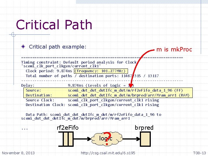
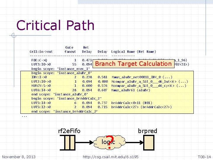
Critical Path Critical path example: m is mk. Proc ===================================== Timing constraint: Default period analysis for Clock 'scemi_clk_port_clkgen/current_clk 1' Clock period: 9. 874 ns (frequency: 101. 277 MHz) Total number of paths / destination ports: 114672315 / 13117 ------------------------------------Delay: 9. 874 ns (Levels of Logic = 17) Source: scemi_dut_dut. Ifc_m_dut/m/rf 2 e. Fifo_data_1_96 (FF) Destination: scemi_dut_dut. Ifc_m_dut/m/brpred/arr/Mram_arr 1 (RAM) Source Clock: scemi_clk_port_clkgen/current_clk 1 rising Destination Clock: scemi_clk_port_clkgen/current_clk 1 rising Data Path: scemi_dut_dut. Ifc_m_dut/m/rf 2 e. Fifo_data_1_96 to scemi_dut_dut. Ifc_m_dut/m/brpred/arr/Mram_arr 1. . . rf 2 e. Fifo ? brpred logic November 8, 2013 http: //csg. csail. mit. edu/6. s 195 T 08 -13
Critical Path Gate Net Cell: in->out fanout Delay --------------------FDE: C->Q 1 0. 471 0. 710 LUT 3: I 0 ->O 55 0. 094 0. 468 begin scope: 'instance_exec_1' begin scope: 'instance_alu. Br_0' INV: I->O 2 0. 238 0. 581 LUT 2: I 0 ->O 1 0. 094 0. 000 MUXCY: S->O 1 0. 600 0. 576 LUT 6: I 4 ->O 28 0. 094 0. 607 end scope: 'instance_alu. Br_0' begin scope: 'instance_br. Addr. Calc_2' LUT 5: I 4 ->O 6 0. 094 0. 737 LUT 5: I 2 ->O 2 0. 094 0. 715 end scope: 'instance_br. Addr. Calc_2‘ Logical Name (Net Name) ------rf 2 e. Fifo_data_1_96 (rf 2 e. Fifo_data_1_96) e. RVal 1__h 82702<31>1 (e. RVal 1__h 82702<31>) Branch Target Calculation Mmux_alu. Br_not 00011_INV_0 (. . . ) Mcompar_alu. Br_a_SLE_0___d 6_lut<6 > (. . . ) Mcompar_alu. Br_a_SLE_0___d 6_cy<6 > (. . . ) Mmux_alu. Br 61 (alu. Br) br. Addr. Calc<0>11 (N 01) br. Addr. Calc<27> (br. Addr. Calc<27>) . . . rf 2 e. Fifo ? brpred logic November 8, 2013 http: //csg. csail. mit. edu/6. s 195 T 08 -14
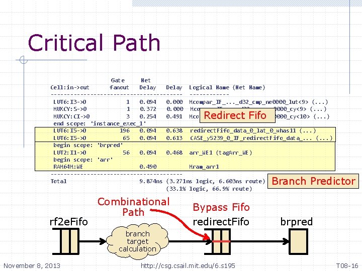
Critical Path Gate Net Cell: in->out fanout Delay Logical Name (Net Name) --------------------LUT 6: I 3 ->O 1 0. 094 0. 000 Mcompar_IF_. . . _d 32_cmp_ne 0000_lut<9> (. . . ) MUXCY: S->O 1 0. 372 0. 000 Mcompar_IF_. . . _d 32_cmp_ne 0000_cy<9> (. . . ) MUXCY: CI->O 3 0. 254 0. 491 Mcompar_IF _. . . _d 32_cmp_ne 0000_cy<10> (. . . ) end scope: 'instance_exec_1' LUT 6: I 5 ->O 196 0. 094 0. 638 redirect. Fifo_data_0_lat_0_whas 11 (. . . ) LUT 6: I 5 ->O 65 0. 094 0. 613 CASE_y 5239_0_IF_redirect. Fifo_data_. . . (. . . ) begin scope: 'brpred' LUT 2: I 1 ->O 56 0. 094 0. 468 arr_WE 1 (tag. Arr_WE) begin scope: 'arr' RAM 64 M: WE 0. 490 Mram_arr 1 --------------------Total 9. 874 ns (3. 271 ns logic, 6. 603 ns route) (33. 1% logic, 66. 9% route) Redirect Fifo Branch Predictor rf 2 e. Fifo ? brpred logic November 8, 2013 http: //csg. csail. mit. edu/6. s 195 T 08 -15
Critical Path Gate Net Cell: in->out fanout Delay Logical Name (Net Name) --------------------LUT 6: I 3 ->O 1 0. 094 0. 000 Mcompar_IF_. . . _d 32_cmp_ne 0000_lut<9> (. . . ) MUXCY: S->O 1 0. 372 0. 000 Mcompar_IF_. . . _d 32_cmp_ne 0000_cy<9> (. . . ) MUXCY: CI->O 3 0. 254 0. 491 Mcompar_IF _. . . _d 32_cmp_ne 0000_cy<10> (. . . ) end scope: 'instance_exec_1' LUT 6: I 5 ->O 196 0. 094 0. 638 redirect. Fifo_data_0_lat_0_whas 11 (. . . ) LUT 6: I 5 ->O 65 0. 094 0. 613 CASE_y 5239_0_IF_redirect. Fifo_data_. . . (. . . ) begin scope: 'brpred' LUT 2: I 1 ->O 56 0. 094 0. 468 arr_WE 1 (tag. Arr_WE) begin scope: 'arr' RAM 64 M: WE 0. 490 Mram_arr 1 --------------------Total 9. 874 ns (3. 271 ns logic, 6. 603 ns route) (33. 1% logic, 66. 9% route) Redirect Fifo Branch Predictor rf 2 e. Fifo Combinational Path Bypass Fifo redirect. Fifo brpred branch target calculation November 8, 2013 http: //csg. csail. mit. edu/6. s 195 T 08 -16
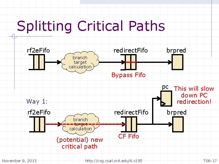
Splitting Critical Paths rf 2 e. Fifo redirect. Fifo brpred branch target calculation Bypass Fifo pc This will slow down PC redirection! Way 1: rf 2 e. Fifo redirect. Fifo brpred branch target calculation (potential) new critical path November 8, 2013 CF Fifo http: //csg. csail. mit. edu/6. s 195 T 08 -17
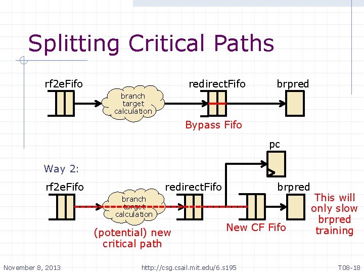
Splitting Critical Paths rf 2 e. Fifo redirect. Fifo brpred branch target calculation Bypass Fifo pc Way 2: rf 2 e. Fifo redirect. Fifo brpred branch target calculation (potential) new critical path November 8, 2013 New CF Fifo http: //csg. csail. mit. edu/6. s 195 This will only slow brpred training T 08 -18
Critical Path After splitting the critical path with way 1: ===================================== Timing constraint: Default period analysis for Clock 'scemi_clk_port_clkgen/current_clk 1' Clock period: 8. 749 ns (frequency: 114. 294 MHz) Total number of paths / destination ports: 38299383 / 13320 ------------------------------------Delay: 8. 749 ns (Levels of Logic = 19) Source: scemi_dut_dut. Ifc_m_dut/m/rf 2 e. Fifo_data_1_96 (FF) Destination: scemi_dut_dut. Ifc_m_dut/m/rf 2 e. Fifo_enq. En_rl (FF) Source Clock: scemi_clk_port_clkgen/current_clk 1 rising Destination Clock: scemi_clk_port_clkgen/current_clk 1 rising Data Path: scemi_dut_dut. Ifc_m_dut/m/rf 2 e. Fifo_data_1_96 to scemi_dut_dut. Ifc_m_dut/m/rf 2 e. Fifo+enq. En+rl rf 2 e. Fifo redirect. Fifo brpred branch target calculation November 8, 2013 CF Fifo http: //csg. csail. mit. edu/6. s 195 T 08 -19
Xilinx Reports *. srp RTL *. bsv Bluespec Compiler *. v HDL Compiler *. par *. twr 01001 01101 01… November 8, 2013 *_map. mrp Timing Analysis Final Design Bitgen Mapping NCD Place & Route http: //csg. csail. mit. edu/6. s 195 FPGA Slice T 08 -20
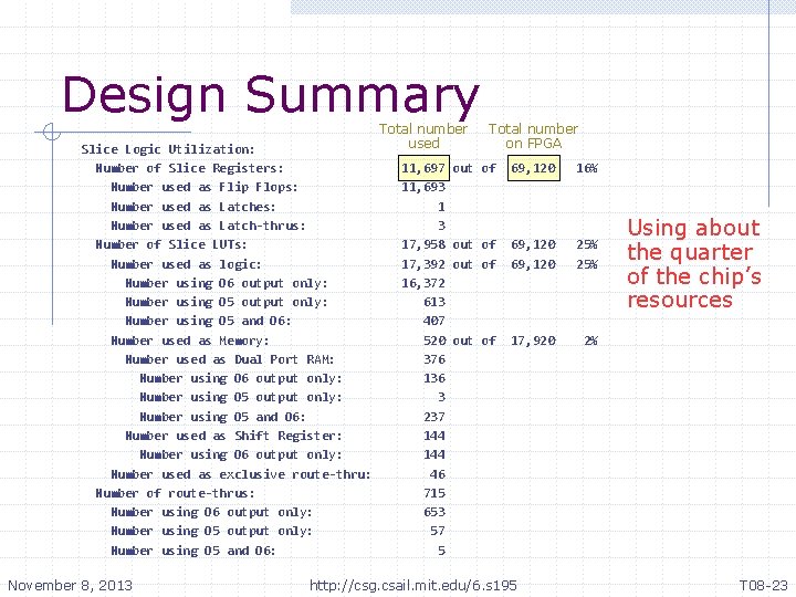
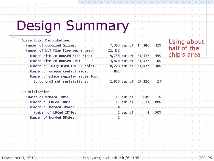
mk. Bridge_map. mrp Search for: “Design Summary” n n November 8, 2013 You’ll see how much of the FPGAs resources are being used by your designs. This information reveals how big your design is and how much routing congestion to expect. http: //csg. csail. mit. edu/6. s 195 T 08 -21
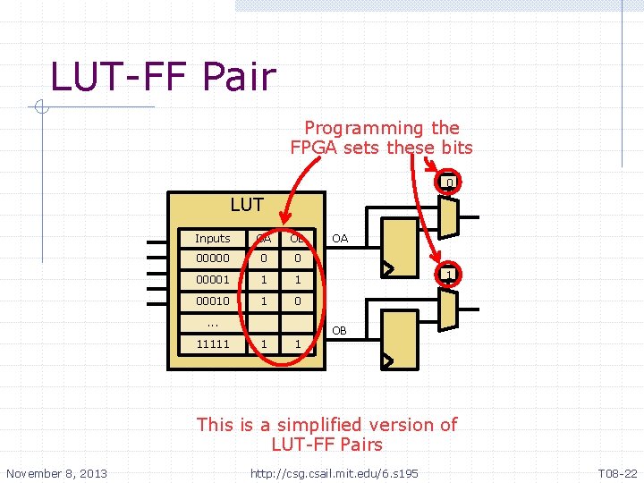
LUT-FF Pair Programming the FPGA sets these bits 0 LUT Inputs OA OB 00000 0 0 00001 1 1 00010 1 0 . . . 11111 OA 1 OB 1 1 This is a simplified version of LUT-FF Pairs November 8, 2013 http: //csg. csail. mit. edu/6. s 195 T 08 -22
Design Summary Slice Logic Utilization: Number of Slice Registers: Number used as Flip Flops: Number used as Latches: Number used as Latch-thrus: Number of Slice LUTs: Number used as logic: Number using O 6 output only: Number using O 5 and O 6: Number used as Memory: Number used as Dual Port RAM: Number using O 6 output only: Number using O 5 and O 6: Number used as Shift Register: Number using O 6 output only: Number used as exclusive route-thru: Number of route-thrus: Number using O 6 output only: Number using O 5 and O 6: November 8, 2013 Total number used Total number on FPGA 11, 697 11, 693 1 3 17, 958 17, 392 16, 372 613 407 520 376 136 3 237 144 46 715 653 57 5 out of 69, 120 16% out of 69, 120 25% out of 17, 920 2% http: //csg. csail. mit. edu/6. s 195 Using about the quarter of the chip’s resources T 08 -23
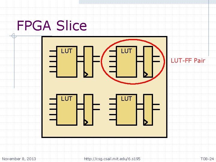
FPGA Slice LUT LUT-FF Pair LUT November 8, 2013 LUT http: //csg. csail. mit. edu/6. s 195 T 08 -24
Design Summary Slice Logic Distribution: Number of occupied Slices: Number of LUT Flip Flop pairs used: Number with an unused Flip Flop: Number with an unused LUT: Number of fully used LUT-FF pairs: Number of unique control sets: Number of slice register sites lost to control set restrictions: IO Utilization: Number of bonded IOBs: Number of LOCed IOBs: Number of bonded IPADs: Number of LOCed IPADs: Number of bonded OPADs: November 8, 2013 7, 385 21, 432 9, 735 3, 474 8, 223 881 out of 17, 280 42% out of 21, 432 45% 16% 38% 1, 953 out of 69, 120 2% 11 out of 4 2 out of 2 640 11 1% 100% 4 50% http: //csg. csail. mit. edu/6. s 195 Using about half of the chip’s area T 08 -25
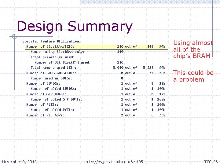
Design Summary Specific Feature Utilization: Number of Block. RAM/FIFO: Number using Block. RAM only: Total primitives used: Number of 36 k Block. RAM used: Total Memory used (KB): Number of BUFG/BUFGCTRLs: Number used as BUFGs: Number of BUFDSs: Number of LOCed BUFDSs: Number of GTP_DUALs: Number of LOCed GTP_DUALs: Number of PCIEs: Number of LOCed PCIEs: Number of PLL_ADVs: November 8, 2013 140 out of 140 5, 040 8 8 1 1 1 2 out of out out of of http: //csg. csail. mit. edu/6. s 195 148 94% 5, 328 32 94% 25% 8 1 1 1 6 12% 100% 33% Using almost all of the chip’s BRAM This could be a problem T 08 -26
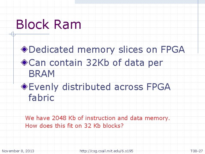
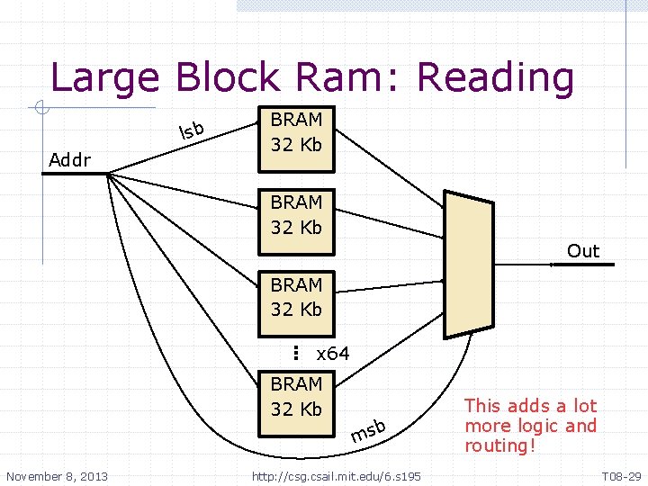
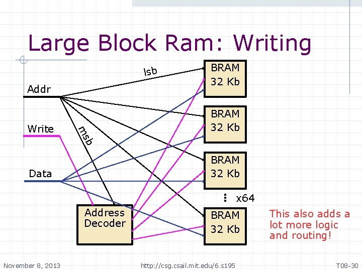
Block Ram Dedicated memory slices on FPGA Can contain 32 Kb of data per BRAM Evenly distributed across FPGA fabric We have 2048 Kb of instruction and data memory. How does this fit on 32 Kb blocks? November 8, 2013 http: //csg. csail. mit. edu/6. s 195 T 08 -27
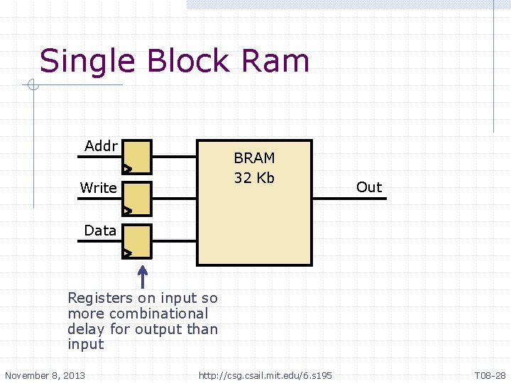
Single Block Ram Addr BRAM 32 Kb Write Out Data Registers on input so more combinational delay for output than input November 8, 2013 http: //csg. csail. mit. edu/6. s 195 T 08 -28
Large Block Ram: Reading lsb Addr BRAM 32 Kb Out BRAM 32 Kb x 64 BRAM 32 Kb November 8, 2013 b ms http: //csg. csail. mit. edu/6. s 195 This adds a lot more logic and routing! T 08 -29
Large Block Ram: Writing lsb Addr b ms Write BRAM 32 Kb Data x 64 Address Decoder November 8, 2013 BRAM 32 Kb http: //csg. csail. mit. edu/6. s 195 This also adds a lot more logic and routing! T 08 -30
Xilinx Reports *. srp RTL *. bsv Bluespec Compiler *. v HDL Compiler *. par *. twr 01001 01101 01… November 8, 2013 *_map. mrp Timing Analysis Final Design Bitgen Mapping NCD Place & Route http: //csg. csail. mit. edu/6. s 195 FPGA Slice T 08 -31
mk. Bridge. par Search for: “Deive Utilization Summary” n November 8, 2013 You’ll see a more accurate report of resource utilization http: //csg. csail. mit. edu/6. s 195 T 08 -32
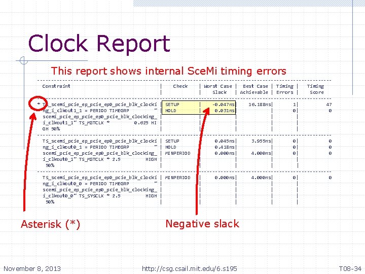
mk. Bridge_map. mrp Search for: “Generating Clock Report” n n November 8, 2013 You’ll see some information about clock timing constraints All of these constraints relate to internal Sce. Mi clocks http: //csg. csail. mit. edu/6. s 195 T 08 -33
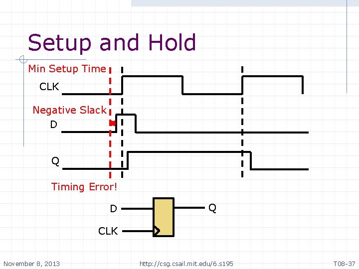
Clock Report This report shows internal Sce. Mi timing errors -----------------------------------------------------Constraint | Check | Worst Case | Best Case | Timing | | Slack | Achievable | Errors | Score -----------------------------------------------------* TS_scemi_pcie_ep 0_pcie_blk_clocki | SETUP | -0. 047 ns| 16. 188 ns| 1| 47 ng_i_clkout 1_1 = PERIOD TIMEGRP " | HOLD | 0. 031 ns| | 0| 0 scemi_pcie_ep 0_pcie_blk_clocking_ | | | i_clkout 1_1" TS_MGTCLK * 0. 625 HI | | | GH 50% | | | -----------------------------------------------------TS_scemi_pcie_ep 0_pcie_blk_clocki | SETUP | 0. 045 ns| 3. 955 ns| 0| 0 ng_i_clkout 0_1 = PERIOD TIMEGRP " | HOLD | 0. 418 ns| | 0| 0 scemi_pcie_ep 0_pcie_blk_clocking_ | MINPERIOD | 0. 000 ns| 4. 000 ns| 0| 0 i_clkout 0_1" TS_MGTCLK * 2. 5 HIGH | | | 50% | | | -----------------------------------------------------TS_scemi_pcie_ep 0_pcie_blk_clocki | MINPERIOD | 0. 000 ns| 4. 000 ns| 0| 0 ng_i_clkout 0_0 = PERIOD TIMEGRP " | | | scemi_pcie_ep 0_pcie_blk_clocking_ | | | i_clkout 0_0" TS_SYSCLK * 2. 5 HIGH | | | 50% | | | Asterisk (*) November 8, 2013 Negative slack http: //csg. csail. mit. edu/6. s 195 T 08 -34
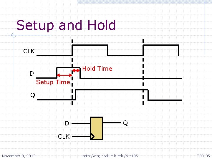
Setup and Hold CLK Hold Time D Setup Time Q D Q CLK November 8, 2013 http: //csg. csail. mit. edu/6. s 195 T 08 -35
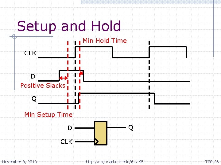
Setup and Hold Min Hold Time CLK D Positive Slacks Q Min Setup Time D Q CLK November 8, 2013 http: //csg. csail. mit. edu/6. s 195 T 08 -36
Setup and Hold Min Setup Time CLK Negative Slack D Q Timing Error! D Q CLK November 8, 2013 http: //csg. csail. mit. edu/6. s 195 T 08 -37
Xilinx Reports *. srp RTL *. bsv Bluespec Compiler *. v HDL Compiler *. par *. twr 01001 01101 01… November 8, 2013 *_map. mrp Timing Analysis Final Design Bitgen Mapping NCD Place & Route http: //csg. csail. mit. edu/6. s 195 FPGA Slice T 08 -38
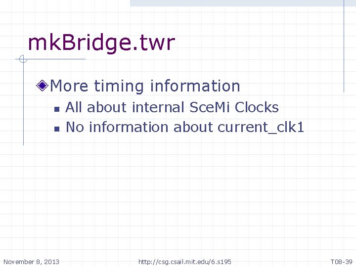
mk. Bridge. twr More timing information n n November 8, 2013 All about internal Sce. Mi Clocks No information about current_clk 1 http: //csg. csail. mit. edu/6. s 195 T 08 -39
Conclusion Any Questions? November 8, 2013 http: //csg. csail. mit. edu/6. s 195 T 08 -40
‘build’ utility Automates the Xilinx tool flow See `build --doc` for more information November 8, 2013 http: //csg. csail. mit. edu/6. s 195 T 08 -41
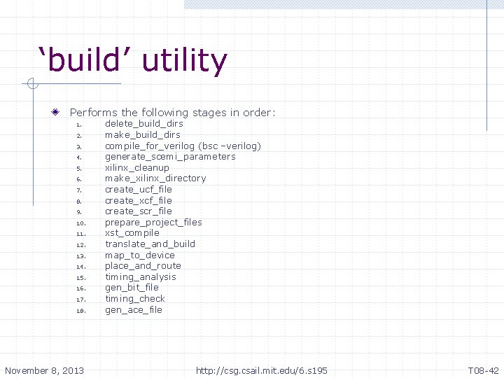
‘build’ utility Performs the following stages in order: 1. 2. 3. 4. 5. 6. 7. 8. 9. 10. 11. 12. 13. 14. 15. 16. 17. 18. November 8, 2013 delete_build_dirs make_build_dirs compile_for_verilog (bsc –verilog) generate_scemi_parameters xilinx_cleanup make_xilinx_directory create_ucf_file create_xcf_file create_scr_file prepare_project_files xst_compile translate_and_build map_to_device place_and_route timing_analysis gen_bit_file timing_check gen_ace_file http: //csg. csail. mit. edu/6. s 195 T 08 -42
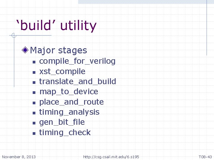
‘build’ utility Major stages n n n n November 8, 2013 compile_for_verilog xst_compile translate_and_build map_to_device place_and_route timing_analysis gen_bit_file timing_check http: //csg. csail. mit. edu/6. s 195 T 08 -43