CPLD Vs FPGA Positioning Presentation LATTICE SEMICONDUCTOR CORPORATION

- Slides: 25

CPLD Vs. FPGA Positioning Presentation © LATTICE SEMICONDUCTOR CORPORATION CPLD VS FPGA February, 02 1

Agenda • Architecture Descriptions – CPLD – FPGA – Advantages / Disadvantages • Gate Counting • Common Terms • Positioning © LATTICE SEMICONDUCTOR CORPORATION CPLD VS FPGA February, 02 2

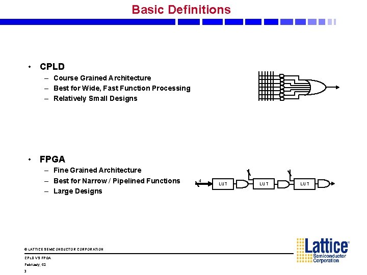
Basic Definitions • CPLD – Course Grained Architecture – Best for Wide, Fast Function Processing – Relatively Small Designs • FPGA – Fine Grained Architecture – Best for Narrow / Pipelined Functions – Large Designs © LATTICE SEMICONDUCTOR CORPORATION CPLD VS FPGA February, 02 3 4 LUT LUT

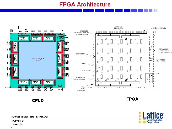
Input Bus Generic Logic Block February, 02 TCK TMS I/O 72 I/O 73 I/O 74 I/O 75 I/O 92 I/O 93 I/O 94 I/O 95 I/O 96 I/O 97 I/O 98 I/O 99 I/O 116 I/O 117 I/O 118 I/O 119 I/O 120 I/O 121 I/O 122 I/O 123 I/O 140 I/O 141 I/O 142 I/O 143 CLK 0 CLK 1 1 1 CLK 2 CLK 3 I/O 147 I/O 146 I/O 145 I/O 144 I/O 167 I/O 166 I/O 165 I/O 164 Input Bus © LATTICE SEMICONDUCTOR CORPORATION CPLD VS FPGA TDI TDO Generic Logic Block CPLD 4 I/O 68 I/O 69 I/O 70 I/O 71 I/O 48 I/O 49 I/O 50 I/O 51 I/O 44 I/O 45 I/O 46 I/O 47 Input Bus I/O 171 I/O 170 I/O 169 I/O 168 I/O 195 I/O 194 I/O 193 I/O 192 I/O 215 I/O 214 I/O 213 I/O 212 Input Bus SET/RESET Generic Logic Block I/O 191 I/O 190 I/O 189 I/O 188 Input Bus Generic Logic Block Input Bus I/O 219 I/O 218 I/O 217 I/O 216 Generic Logic Block I/O 239 I/O 238 I/O 237 I/O 236 Global Routing Pool (GRP) Input Bus I/O 243 I/O 242 I/O 241 I/O 240 Generic Logic Block I/O 263 I/O 262 I/O 261 I/O 260 Boundary Scan Interface Input Bus I/O 267 I/O 266 I/O 265 I/O 264 Input Bus Generic Logic Block I/O 287 I/O 286 I/O 285 I/O 284 Input Bus Generic Logic Block VCCIO I/O 24 I/O 25 I/O 26 I/O 27 I/O 20 I/O 21 I/O 22 I/O 23 GOE 0 GOE 1 I/O 0 / TOE I/O 1 I/O 2 I/O 3 FPGA Architecture FPGA

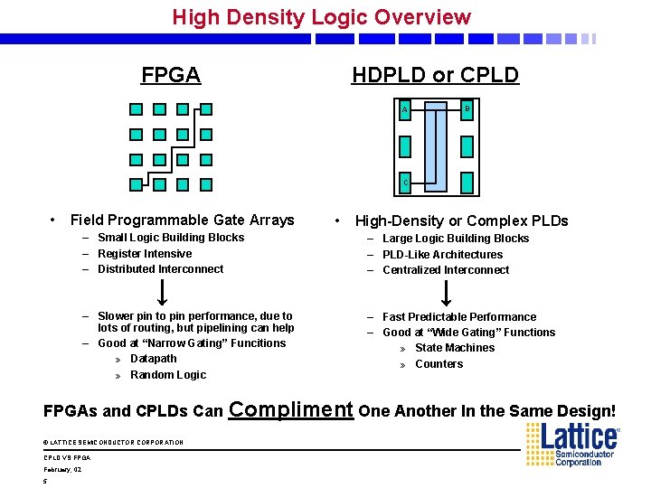
High Density Logic Overview FPGA HDPLD or CPLD A B C • Field Programmable Gate Arrays • High-Density or Complex PLDs – Small Logic Building Blocks – Register Intensive – Distributed Interconnect – Large Logic Building Blocks – PLD-Like Architectures – Centralized Interconnect – Slower pin to pin performance, due to lots of routing, but pipelining can help – Good at “Narrow Gating” Funcitions » Datapath » Random Logic – Fast Predictable Performance – Good at “Wide Gating” Functions » State Machines » Counters FPGAs and CPLDs Can Compliment One Another In the Same Design! © LATTICE SEMICONDUCTOR CORPORATION CPLD VS FPGA February, 02 5

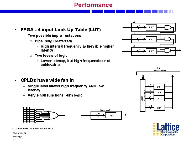
Performance LE 4 • FPGA - 4 input Look Up Table (LUT) – Two possible implementations » Pipelining (preferred) • High internal frequency achievable higher latency » Two levels of logic • Lower latency, but high frequencies not achievable LUT LE 4 LUT Row Interconnect • CPLDs have wide fan in 4 Local Interconnect – Single level allows high frequency AND low latency – Very small functions burn logic 4 4 4 Macrocell 68 © LATTICE SEMICONDUCTOR CORPORATION CPLD VS FPGA February, 02 6 Logic LUT LUT

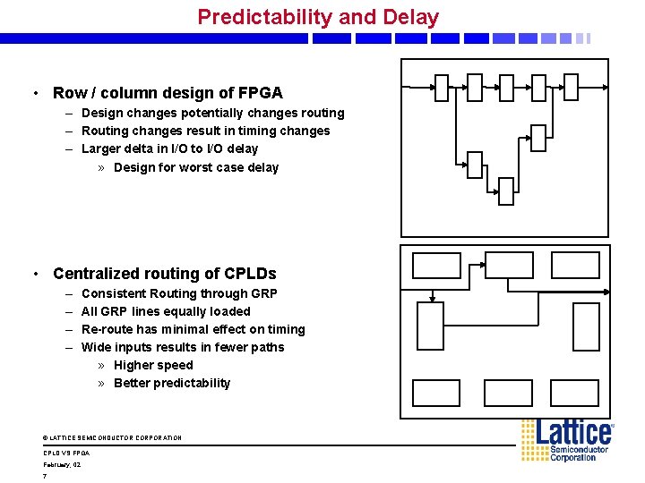
Predictability and Delay • Row / column design of FPGA – Design changes potentially changes routing – Routing changes result in timing changes – Larger delta in I/O to I/O delay » Design for worst case delay • Centralized routing of CPLDs – – Consistent Routing through GRP All GRP lines equally loaded Re-route has minimal effect on timing Wide inputs results in fewer paths » Higher speed » Better predictability © LATTICE SEMICONDUCTOR CORPORATION CPLD VS FPGA February, 02 7

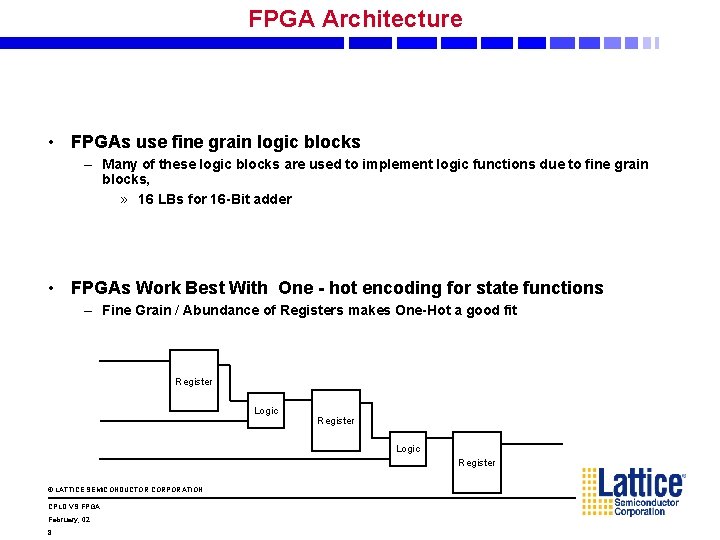
FPGA Architecture • FPGAs use fine grain logic blocks – Many of these logic blocks are used to implement logic functions due to fine grain blocks, » 16 LBs for 16 -Bit adder • FPGAs Work Best With One - hot encoding for state functions – Fine Grain / Abundance of Registers makes One-Hot a good fit Register Logic Register © LATTICE SEMICONDUCTOR CORPORATION CPLD VS FPGA February, 02 8

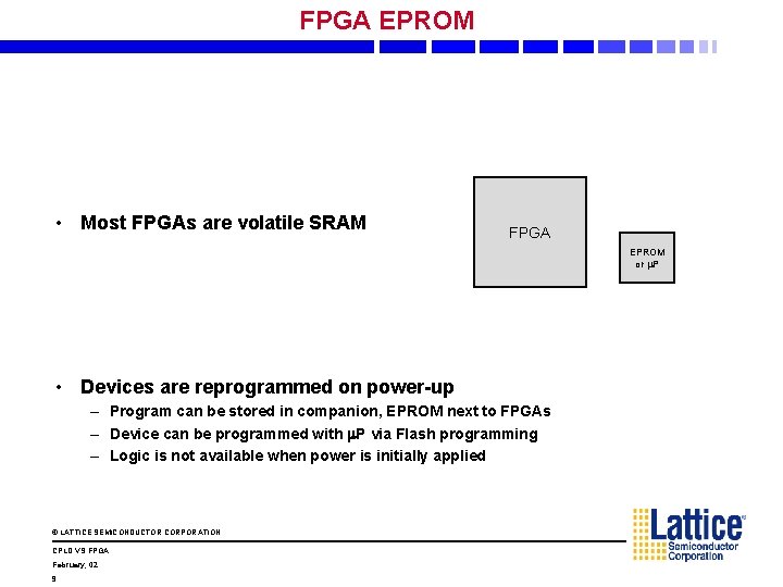
FPGA EPROM • Most FPGAs are volatile SRAM FPGA EPROM or P • Devices are reprogrammed on power-up – Program can be stored in companion, EPROM next to FPGAs – Device can be programmed with P via Flash programming – Logic is not available when power is initially applied © LATTICE SEMICONDUCTOR CORPORATION CPLD VS FPGA February, 02 9

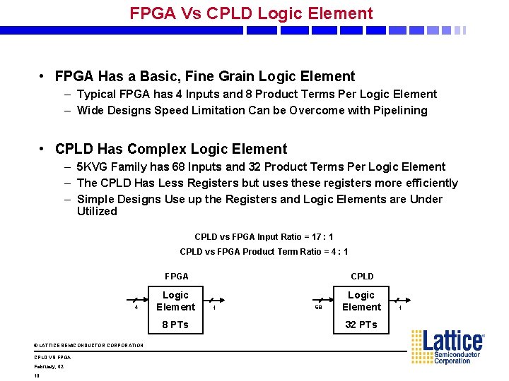
FPGA Vs CPLD Logic Element • FPGA Has a Basic, Fine Grain Logic Element – Typical FPGA has 4 Inputs and 8 Product Terms Per Logic Element – Wide Designs Speed Limitation Can be Overcome with Pipelining • CPLD Has Complex Logic Element – 5 KVG Family has 68 Inputs and 32 Product Terms Per Logic Element – The CPLD Has Less Registers but uses these registers more efficiently – Simple Designs Use up the Registers and Logic Elements are Under Utilized CPLD vs FPGA Input Ratio = 17 : 1 CPLD vs FPGA Product Term Ratio = 4 : 1 4 FPGA CPLD Logic Element 8 PTs © LATTICE SEMICONDUCTOR CORPORATION CPLD VS FPGA February, 02 10 1 68 32 PTs 1

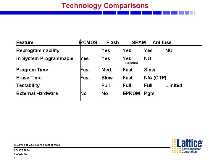
Technology Comparisons Feature E 2 CMOS Reprogrammability Flash SRAM Antifuse Yes Yes NO In-System Programmable Yes Yes NO Program Time Fast Med. Fast Slow Erase Time Fast Slow Fast N/A (OTP) Full No EPROM Pgmr Testability External Hardware © LATTICE SEMICONDUCTOR CORPORATION CPLD VS FPGA February, 02 11 No (Volatile) Limited

Gate Counting © LATTICE SEMICONDUCTOR CORPORATION CPLD VS FPGA February, 02 12

CPLD Vs. FPGA Fitting • Number of PLD Gates or Registers Doesn’t Tell the Entire Story, The Application Does – Even among equivalent product types, Gate count is “specsmanship”, the only real way to see if a design will fit or fit better is to run it! • Applications Needing High Speed and Predictability Should Use CPLD • Large Register Intensive Logic Applications Should Use FPGA • Most Designs Have a Mixture of Qualities that Could Fit Either, So Both CPLD and FPGA Should Be Considered © LATTICE SEMICONDUCTOR CORPORATION CPLD VS FPGA February, 02 13

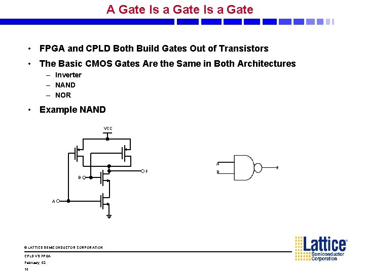
A Gate Is a Gate • FPGA and CPLD Both Build Gates Out of Transistors • The Basic CMOS Gates Are the Same in Both Architectures – Inverter – NAND – NOR • Example NAND VCC A F B A © LATTICE SEMICONDUCTOR CORPORATION CPLD VS FPGA February, 02 14 B F

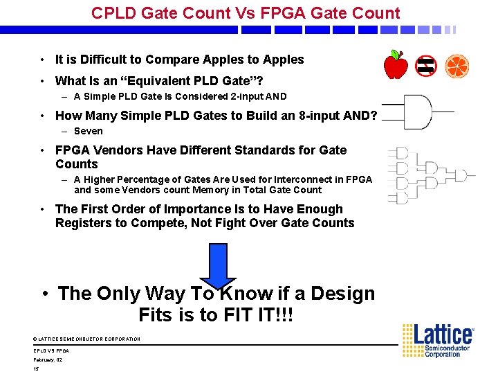
CPLD Gate Count Vs FPGA Gate Count • It is Difficult to Compare Apples to Apples • What Is an “Equivalent PLD Gate”? – A Simple PLD Gate Is Considered 2 -input AND • How Many Simple PLD Gates to Build an 8 -input AND? – Seven • FPGA Vendors Have Different Standards for Gate Counts – A Higher Percentage of Gates Are Used for Interconnect in FPGA and some Vendors count Memory in Total Gate Count • The First Order of Importance Is to Have Enough Registers to Compete, Not Fight Over Gate Counts • The Only Way To Know if a Design Fits is to FIT IT!!! © LATTICE SEMICONDUCTOR CORPORATION CPLD VS FPGA February, 02 15

Terms © LATTICE SEMICONDUCTOR CORPORATION CPLD VS FPGA February, 02 16

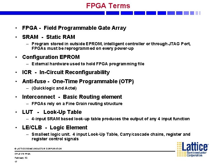
FPGA Terms • FPGA - Field Programmable Gate Array • SRAM - Static RAM – Program stored in outside EPROM, intelligent controller or through JTAG Port, FPGAs must be reprogrammed on every power-up • Configuration EPROM – External hardware used to hold FPGA programming file • ICR - In-Circuit Reconfigurability • Anti-fuse - One-Time Programmable (OTP) – (Quicklogic and Actel) • Interconnect - Basic Routing element – FPGAs rely on a Fine Grain routing structure • LUT - Look-Up Table – 4 -input SRAM based look-up table produces the output of any 4 input function • LE/CLB - Logic Element – Smallest logic unit. 4 input Look-Up Table, Carry/cascade chains, register and register control signals © LATTICE SEMICONDUCTOR CORPORATION CPLD VS FPGA February, 02 17

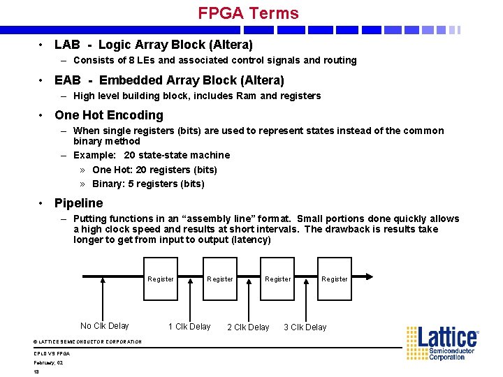
FPGA Terms • LAB - Logic Array Block (Altera) – Consists of 8 LEs and associated control signals and routing • EAB - Embedded Array Block (Altera) – High level building block, includes Ram and registers • One Hot Encoding – When single registers (bits) are used to represent states instead of the common binary method – Example: 20 state-state machine » One Hot: 20 registers (bits) » Binary: 5 registers (bits) • Pipeline – Putting functions in an “assembly line” format. Small portions done quickly allows a high clock speed and results at short intervals. The drawback is results take longer to get from input to output (latency) Register No Clk Delay © LATTICE SEMICONDUCTOR CORPORATION CPLD VS FPGA February, 02 18 Register 1 Clk Delay Register 2 Clk Delay Register 3 Clk Delay

FPGA Terms • So. C – System on a Chip • MPI – Microprocessor Interface • EBR – Embedded Block RAM • PLC – Programmable Logic Cell • PIO – Programmable Input/Output Cells • CIB – Common Interface Block • PFU – Programmable Function Unit • SLIC – Decoder / PAL like logic © LATTICE SEMICONDUCTOR CORPORATION CPLD VS FPGA February, 02 19

Positioning © LATTICE SEMICONDUCTOR CORPORATION CPLD VS FPGA February, 02 20

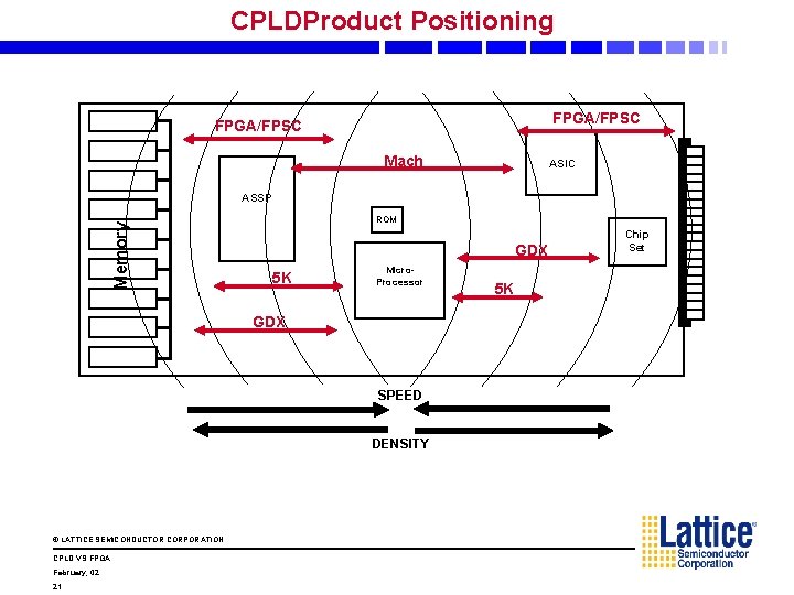
CPLDProduct Positioning FPGA/FPSC Mach ASIC Memory ASSP ROM GDX 5 K Micro. Processor GDX SPEED DENSITY © LATTICE SEMICONDUCTOR CORPORATION CPLD VS FPGA February, 02 21 5 K Chip Set

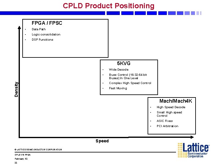
CPLD Product Positioning FPGA / FPSC • Data Path • Logic consolidation • DSP Functions Density 5 KVG • Wide Decode • Buss Control (16 -32 -64 bit Buses) In One Level • Complex High Speed Control • Fast Muxing Mach/Mach 4 K Speed © LATTICE SEMICONDUCTOR CORPORATION CPLD VS FPGA February, 02 22 • High Speed Decode • Small High speed Control • ASIC Fixes • PCI Arbitration

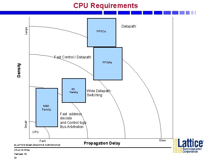
CPU Requirements Large Datapath FPSCs Fast Control / Datapath Density FPGAs 5 K Family Wide Datapath Switching M 4 K Family Small Fast address decode and Control logic Bus Arbitration CPU Fast © LATTICE SEMICONDUCTOR CORPORATION CPLD VS FPGA February, 02 23 Propagation Delay Slow

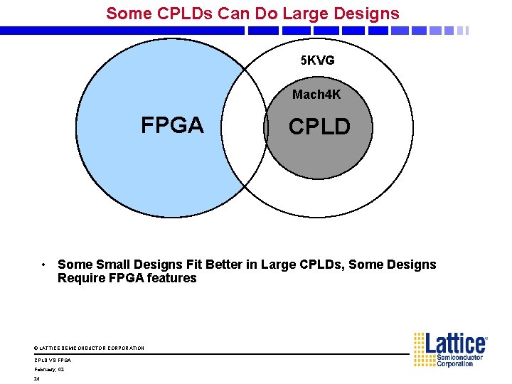
Some CPLDs Can Do Large Designs 5 KVG Mach 4 K FPGA CPLD • Some Small Designs Fit Better in Large CPLDs, Some Designs Require FPGA features © LATTICE SEMICONDUCTOR CORPORATION CPLD VS FPGA February, 02 24

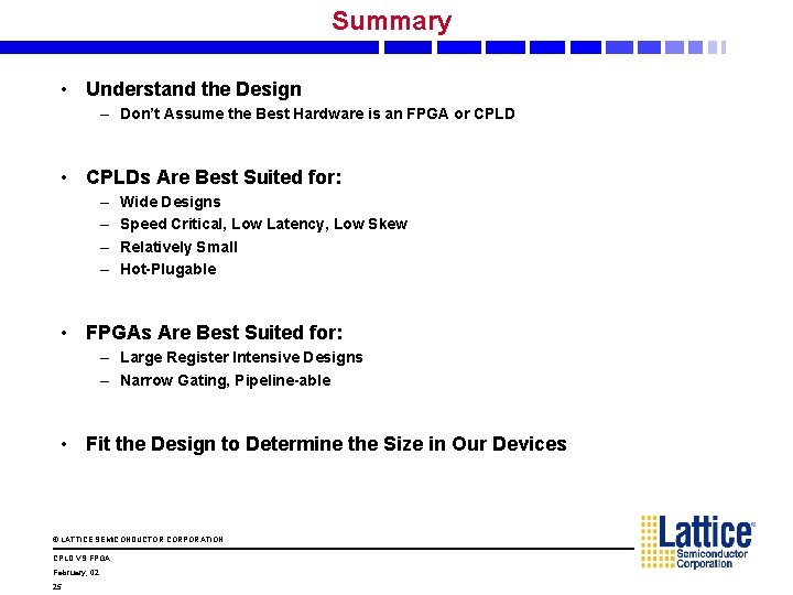
Summary • Understand the Design – Don’t Assume the Best Hardware is an FPGA or CPLD • CPLDs Are Best Suited for: – – Wide Designs Speed Critical, Low Latency, Low Skew Relatively Small Hot-Plugable • FPGAs Are Best Suited for: – Large Register Intensive Designs – Narrow Gating, Pipeline-able • Fit the Design to Determine the Size in Our Devices © LATTICE SEMICONDUCTOR CORPORATION CPLD VS FPGA February, 02 25