
Power Management for Altera Stratix V FPGA Power


- Slides: 21
Power Management for Altera Stratix V
FPGA Power Requirements
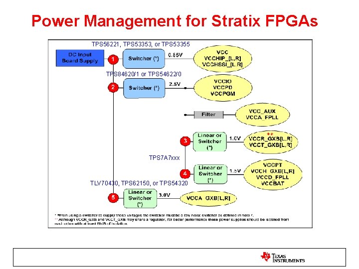
Power Management for Stratix FPGAs TPS 56221, TPS 53353, or TPS 53355 TPS 84620/1 or TPS 54622/0 TPS 7 A 7 xxx TLV 70430, TPS 62150, or TPS 54320
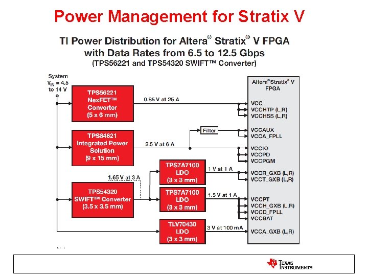
Power Management for Stratix V
FPGA Core and I/O Power
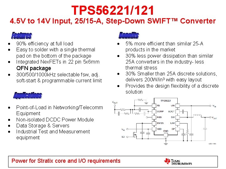
TPS 56221/121 4. 5 V to 14 V Input, 25/15 -A, Step-Down SWIFT™ Converter · · · · 90% efficiency at full load Easy to solder with a single thermal pad on the bottom of the package Integrated Nex. FETs in 22 pin 5 x 6 mm QFN package 300/500/1000 k. Hz selectable fsw, adj. soft-start & programmable current limit · · Point-of-Load in Networking/Telecomm Equipment Non-isolated DCDC Power Module Data Storage & Servers Industrial Test and Measurement equipment Power for Stratix core and I/O requirements 5% more efficient than similar 25 -A products in the market 30% less power dissipation than similar 25 A converters in the industry- less thermal stress 30% Smaller than 25 A discrete solutions, delivers 200 W/in 3 with easy layout Provides the design flexibility of a discrete solution
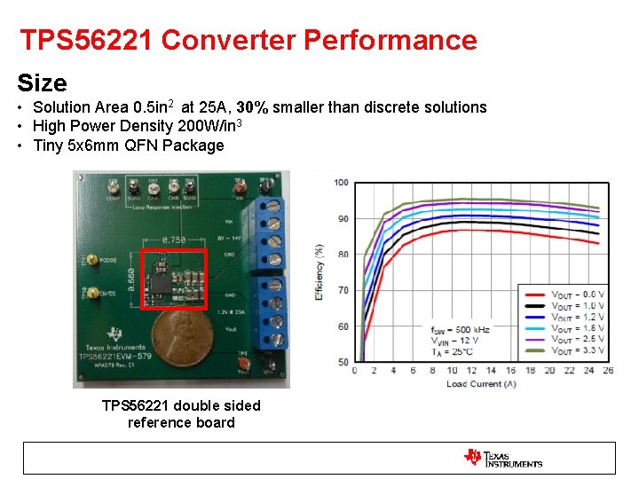
TPS 56221 Converter Performance Size mm • Solution Area 0. 5 in 2 at 25 A, 30% smaller than discrete solutions • High Power Density 200 W/in 3 • Tiny 5 x 6 mm QFN Package TPS 56221 double sided reference board
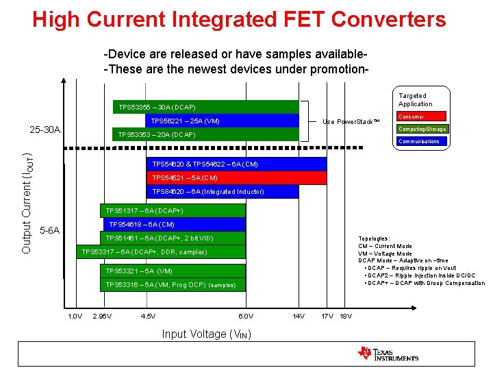
High Current Integrated FET Converters -Device are released or have samples available-These are the newest devices under promotion. Targeted Application TPS 53355 – 30 A (DCAP) TPS 56221 – 25 A (VM) Output Current (IOUT) 25 -30 A Use Power. Stack™ Consumer Computing/Storage TPS 53353 – 20 A (DCAP) Communications TPS 54620 & TPS 54622 – 6 A (CM) TPS 54521 – 5 A (CM) TPS 84620 – 6 A (Integrated Inductor) TPS 51317 – 6 A (DCAP+) TPS 54618 – 6 A (CM) 5 -6 A TPS 51461 – 6 A (DCAP+, 2 bit VID) Topologies: CM – Current Mode VM – Voltage Mode DCAP Mode – Adaptive on –time • DCAP – Requires ripple on Vout • DCAP 2 – Ripple injection inside DC/DC • DCAP+ – DCAP with Droop Compensation TPS 53317 – 6 A (DCAP+, DDR, samples) TPS 53321 – 5 A (VM) TPS 53316 – 5 A (VM, Prog OCP) (samples) 1. 0 V 2. 95 V 4. 5 V 6. 0 V Input Voltage (VIN) 14 V 17 V 18 V
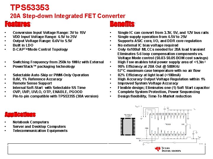
TPS 53353 20 A Step-down Integrated FET Converter Features Benefits • • • Conversion Input Voltage Range: 3 V to 15 V VDD Input Voltage Range: 4. 5 V to 25 V Output Voltage Range: 0. 6 V to 5. 5 V Built in LDO D-CAPTM Mode Control Topology • • Switching Frequency from 250 k to 1 MHz with External Power. Stack™ packaging technology • • Selectable Auto-Skip or PWM-Only Operation 0. 6 V, 1% Reference Accuracy Remote Sense Support Internal Soft-Start with Selectable SS Time OVP, UVLO, OTP, ENABLE, PGOOD Pin-to-pin compatible with TPS 53355 (30 A version) • • • Applications • • • Notebook Computers Server and Desktop Computers Telecommunication Equipments Single IC can convert from 3. 3 V, 5 V, and 12 V bus rails Single supply operation from 4. 5 V to 25 V Supports ASIC core, I/O, and DDR core regulation No external IC bias voltage required Only 4 x 100 u. F MLCCs needed for 20 A load transient Eliminates 5 -6 loop compensation components vs. Voltage Mode control ($0. 03 -$0. 05 BOM cost savings) High Fsw enables total power supply area of <1. 3 in 2 90% Efficiency at 20 A Out @ 500 KHz 57°C maximum case temperature with no air flow 82% Efficiency at light load (<100 m. A) High Accuracy Output Voltage Regulation within 1% Improved System Voltage Accuracy Flexible design; Eliminates one (1) Soft Start capacitor Complete System Protection, Power Sequencing Design flexibility, Time-To-Market reduction
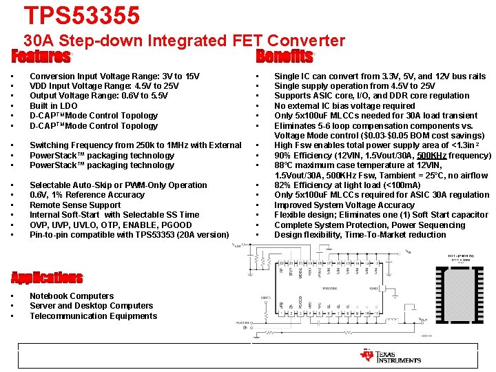
TPS 53355 30 A Step-down Integrated FET Converter Features Benefits • • • Conversion Input Voltage Range: 3 V to 15 V VDD Input Voltage Range: 4. 5 V to 25 V Output Voltage Range: 0. 6 V to 5. 5 V Built in LDO D-CAPTM Mode Control Topology • • • Switching Frequency from 250 k to 1 MHz with External Power. Stack™ packaging technology • • • Selectable Auto-Skip or PWM-Only Operation 0. 6 V, 1% Reference Accuracy Remote Sense Support Internal Soft-Start with Selectable SS Time OVP, UVLO, OTP, ENABLE, PGOOD Pin-to-pin compatible with TPS 53353 (20 A version) • • • Applications • • • Notebook Computers Server and Desktop Computers Telecommunication Equipments Single IC can convert from 3. 3 V, 5 V, and 12 V bus rails Single supply operation from 4. 5 V to 25 V Supports ASIC core, I/O, and DDR core regulation No external IC bias voltage required Only 5 x 100 u. F MLCCs needed for 30 A load transient Eliminates 5 -6 loop compensation components vs. Voltage Mode control ($0. 03 -$0. 05 BOM cost savings) High Fsw enables total power supply area of <1. 3 in 2 90% Efficiency (12 VIN, 1. 5 Vout/30 A, 500 KHz frequency) 88°C maximum case temperature at 12 VIN, 1. 5 Vout/30 A, 500 KHz Fsw, Tambient = 25°C, no airflow 82% Efficiency at light load (<100 m. A) Only 5 x 100 u. F MLCCs required for ASIC 30 A regulation Improved System Voltage Accuracy Flexible design; Eliminates one (1) Soft Start capacitor Complete System Protection, Power Sequencing Design flexibility, Time-To-Market reduction
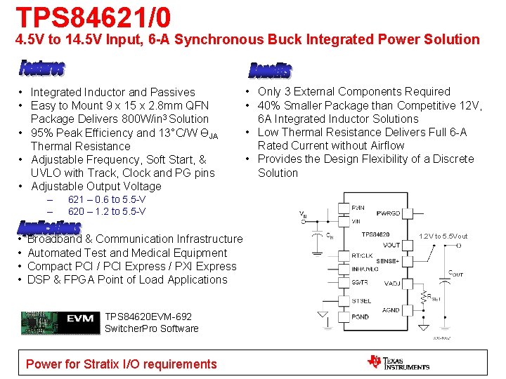
TPS 84621/0 4. 5 V to 14. 5 V Input, 6 -A Synchronous Buck Integrated Power Solution • Integrated Inductor and Passives • Easy to Mount 9 x 15 x 2. 8 mm QFN Package Delivers 800 W/in 3 Solution • 95% Peak Efficiency and 13°C/W ӨJA Thermal Resistance • Adjustable Frequency, Soft Start, & UVLO with Track, Clock and PG pins • Adjustable Output Voltage – – • • • Only 3 External Components Required • 40% Smaller Package than Competitive 12 V, 6 A Integrated Inductor Solutions • Low Thermal Resistance Delivers Full 6 -A Rated Current without Airflow • Provides the Design Flexibility of a Discrete Solution 621 – 0. 6 to 5. 5 -V 620 – 1. 2 to 5. 5 -V Broadband & Communication Infrastructure Automated Test and Medical Equipment Compact PCI / PCI Express / PXI Express DSP & FPGA Point of Load Applications TPS 84620 EVM-692 Switcher. Pro Software Power for Stratix I/O requirements 1. 2 V to 5. 5 Vout
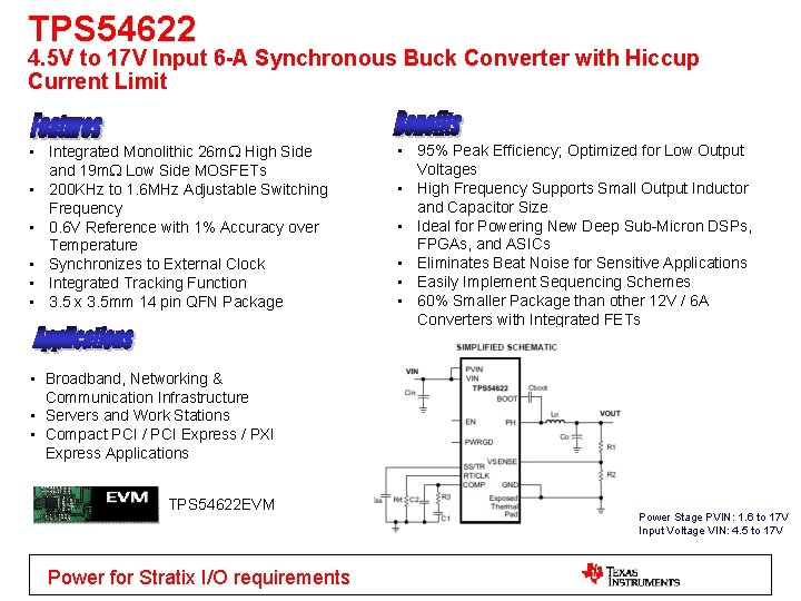
TPS 54622 4. 5 V to 17 V Input 6 -A Synchronous Buck Converter with Hiccup Current Limit • Integrated Monolithic 26 m High Side and 19 m Low Side MOSFETs • 200 KHz to 1. 6 MHz Adjustable Switching Frequency • 0. 6 V Reference with 1% Accuracy over Temperature • Synchronizes to External Clock • Integrated Tracking Function • 3. 5 x 3. 5 mm 14 pin QFN Package • 95% Peak Efficiency; Optimized for Low Output Voltages • High Frequency Supports Small Output Inductor and Capacitor Size • Ideal for Powering New Deep Sub-Micron DSPs, FPGAs, and ASICs • Eliminates Beat Noise for Sensitive Applications • Easily Implement Sequencing Schemes • 60% Smaller Package than other 12 V / 6 A Converters with Integrated FETs • Broadband, Networking & Communication Infrastructure • Servers and Work Stations • Compact PCI / PCI Express / PXI Express Applications TPS 54622 EVM Power for Stratix I/O requirements Power Stage PVIN: 1. 6 to 17 V Input Voltage VIN: 4. 5 to 17 V
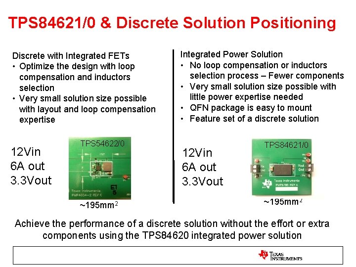
TPS 84621/0 & Discrete Solution Positioning Discrete with Integrated FETs • Optimize the design with loop compensation and inductors selection • Very small solution size possible with layout and loop compensation expertise 12 Vin 6 A out 3. 3 Vout TPS 54622/0 ~195 mm 2 Integrated Power Solution • No loop compensation or inductors selection process – Fewer components • Very small solution size possible with little power expertise needed • QFN package is easy to mount • Feature set of a discrete solution 12 Vin 6 A out 3. 3 Vout TPS 84621/0 ~195 mm 2 Achieve the performance of a discrete solution without the effort or extra components using the TPS 84620 integrated power solution
FPGA Transceiver Power Linear Regulators
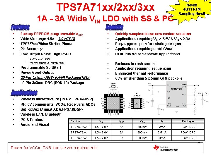
TPS 7 A 71 xx/2 xx/3 xx 1 A - 3 A Wide VIN LDO with SS & PG • • • Factory EEPROM programmable VOUT Wide Vin range 1. 5 V – 7. 0 V(TBD) TPS 737 xx/796 xx Similar Pinout 2% Accuracy Low Output Noise/ High PSRR – – 30 m. VRMS(TBD) PSRR 55 d. B @ 1 k. Hz(TBD) • • Programmable Soft. Start Power Good Output 20 -Pin 5 x 5 mm RGW (QFN) Package(TBD) 10 -Pin 3 x 3 mm DRC (SON 10) Package • • • Wireless Infrastructure (Tx/Rx, FPGA&DSP) RF: 5 V components, VCOs, Receivers, ADCs Set. Top. Box (Amp, AD/DA, FPGA&DSP) Wireless LAN, Bluetooth PC & Printers Device Audio and Visual New!!! 4 Q 11 RTM Sampling Now!! • • • Quickly sample/release new custom versions Applications requiring V IN > 5. 5 V & VIN < 2. 0 V Easy upgrade path for existing designs Applications requiring stable Vout RF/Audio Noise Sensitive Applications • • Reduces in-rush current Application requiring sequencing Enhanced thermal performance 65% smaller than 5 x 5 mm QFN package VIN IOUT VDO IQ Package TPS 7 A 71 xx 1. 5 – 7. 0 V 1 A 100 m. V 2 m. A RGW, DRC TPS 7 A 72 xx 1. 5 – 7. 0 V 2 A 200 m. V 2. 5 m. A RGW, DRC TPS 7 A 73 xx 1. 5 – 7. 0 V 3 A 300 m. V 3 m. A RGW, DRC 15 Power for VCCx_GXB transceiver requirements
VCCA Transceiver Power
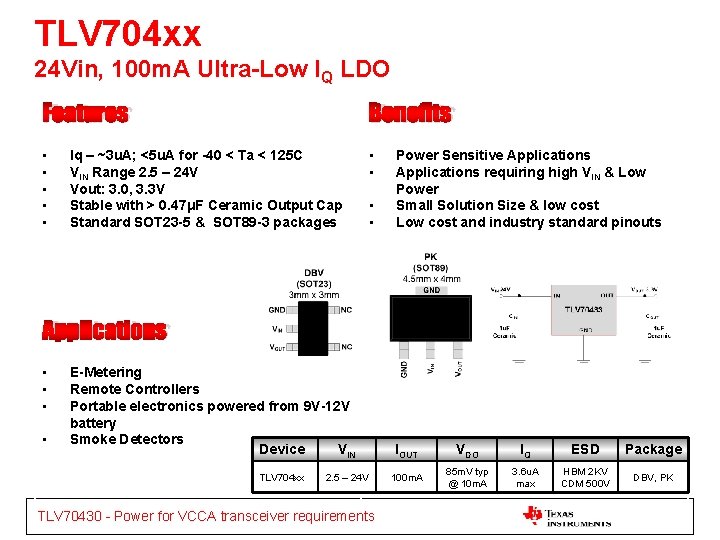
TLV 704 xx 24 Vin, 100 m. A Ultra-Low IQ LDO Features Benefits • • Iq – ~3 u. A; <5 u. A for -40 < Ta < 125 C VIN Range 2. 5 – 24 V Vout: 3. 0, 3. 3 V Stable with > 0. 47μF Ceramic Output Cap Standard SOT 23 -5 & SOT 89 -3 packages • • Power Sensitive Applications requiring high VIN & Low Power Small Solution Size & low cost Low cost and industry standard pinouts Applications • • E-Metering Remote Controllers Portable electronics powered from 9 V-12 V battery Smoke Detectors Device VIN TLV 704 xx 2. 5 – 24 V TLV 70430 - Power for VCCA transceiver requirements IOUT VDO IQ ESD Package 100 m. A 85 m. V typ @ 10 m. A 3. 6 u. A max HBM 2 KV CDM 500 V DBV, PK
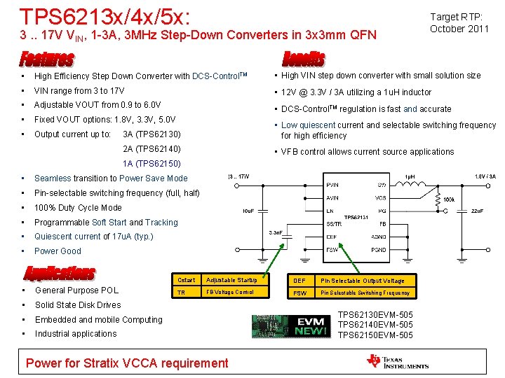
TPS 6213 x/4 x/5 x: 3. . 17 V VIN, 1 -3 A, 3 MHz Step-Down Converters in 3 x 3 mm QFN Target RTP: October 2011 • High Efficiency Step Down Converter with DCS-Control. TM • High VIN step down converter with small solution size • VIN range from 3 to 17 V • 12 V @ 3. 3 V / 3 A utilizing a 1 u. H inductor • Adjustable VOUT from 0. 9 to 6. 0 V • DCS-Control. TM regulation is fast and accurate • Fixed VOUT options: 1. 8 V, 3. 3 V, 5. 0 V • Output current up to: 3 A (TPS 62130) • Low quiescent current and selectable switching frequency for high efficiency 2 A (TPS 62140) • VFB control allows current source applications 1 A (TPS 62150) • Seamless transition to Power Save Mode • Pin-selectable switching frequency (full, half) • 100% Duty Cycle Mode • Programmable Soft Start and Tracking • Quiescent current of 17 u. A (typ. ) • Power Good • General Purpose POL • Solid State Disk Drives • Embedded and mobile Computing • Industrial applications Cstart Adjustable Startup DEF Pin Selectable Output Voltage TR FB Voltage Control FSW Pin Selectable Switching Frequency Power for Stratix VCCA requirement TPS 62130 EVM-505 TPS 62140 EVM-505 TPS 62150 EVM-505
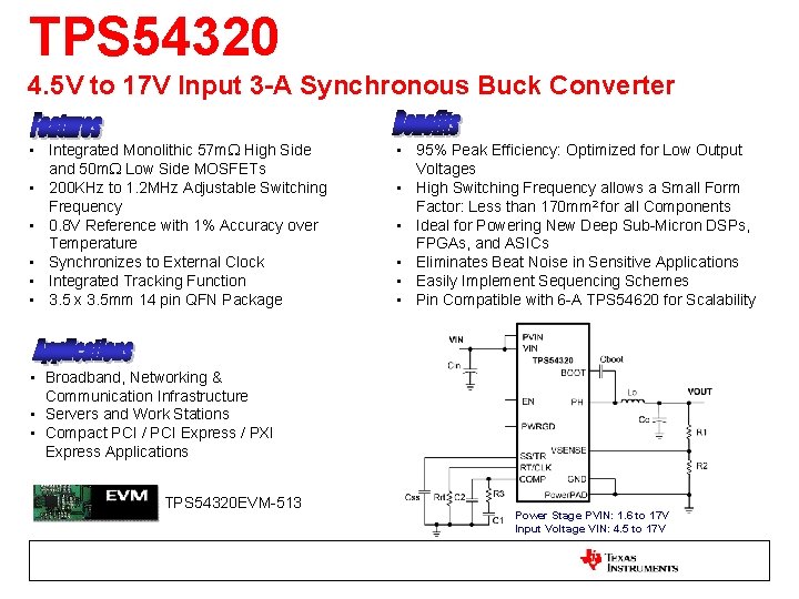
TPS 54320 4. 5 V to 17 V Input 3 -A Synchronous Buck Converter • Integrated Monolithic 57 m High Side and 50 m Low Side MOSFETs • 200 KHz to 1. 2 MHz Adjustable Switching Frequency • 0. 8 V Reference with 1% Accuracy over Temperature • Synchronizes to External Clock • Integrated Tracking Function • 3. 5 x 3. 5 mm 14 pin QFN Package • 95% Peak Efficiency: Optimized for Low Output Voltages • High Switching Frequency allows a Small Form Factor: Less than 170 mm 2 for all Components • Ideal for Powering New Deep Sub-Micron DSPs, FPGAs, and ASICs • Eliminates Beat Noise in Sensitive Applications • Easily Implement Sequencing Schemes • Pin Compatible with 6 -A TPS 54620 for Scalability • Broadband, Networking & Communication Infrastructure • Servers and Work Stations • Compact PCI / PCI Express / PXI Express Applications TPS 54320 EVM-513 Power Stage PVIN: 1. 6 to 17 V Input Voltage VIN: 4. 5 to 17 V
Selection Guide
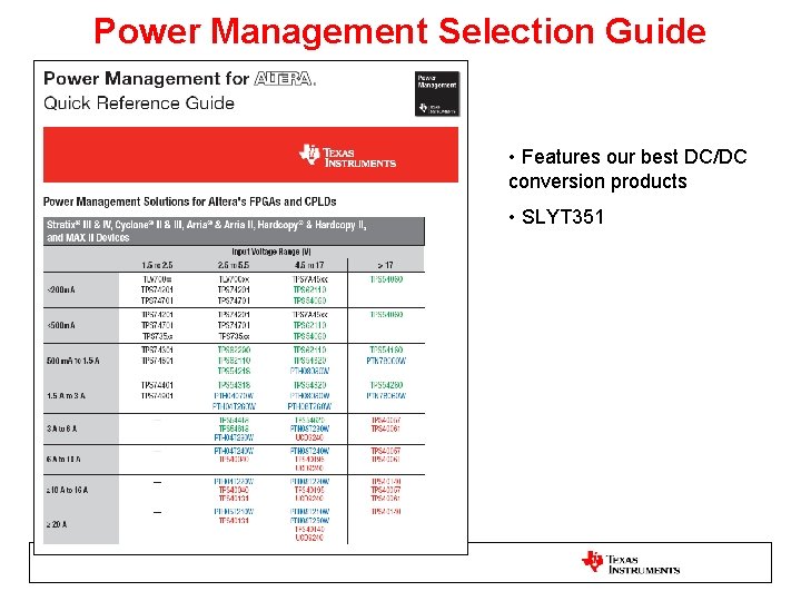
Power Management Selection Guide • Features our best DC/DC conversion products • SLYT 351