Design Techniques for Million Gate High Speed FPGAs

- Slides: 60

Design Techniques for Million Gate, High Speed FPGAs Michael A. Bohm Chief Scientist Technical Fellow Mentor Graphics

Agenda • • The Problem State-of-the-Art Technology Design Issues Performance Oriented Design

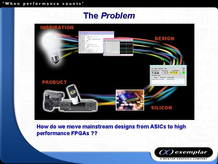
The Problem INSPIRATION DESIGN PRODUCT SILICON How do we move mainstream designs from ASICs to high performance FPGAs ? ?

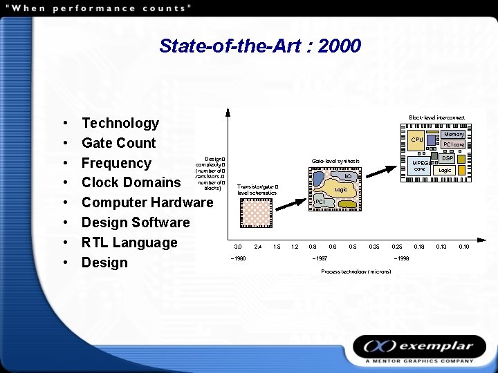
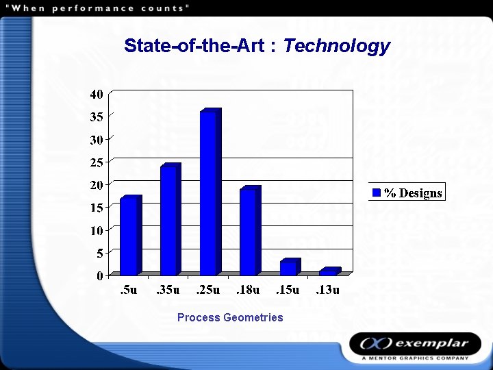
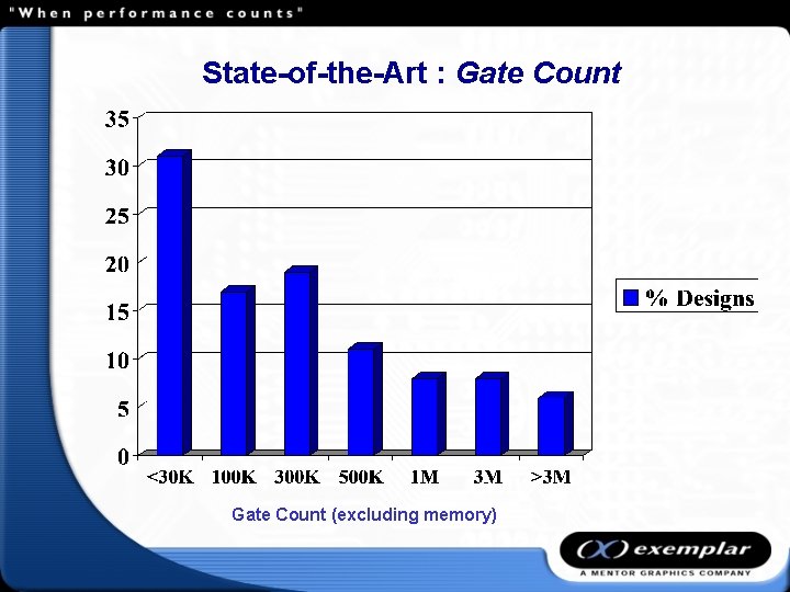
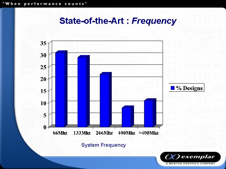
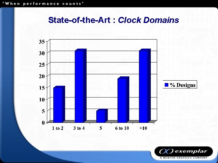
State-of-the-Art : 2000 • • Technology Gate Count Frequency Clock Domains Computer Hardware Design Software RTL Language Design

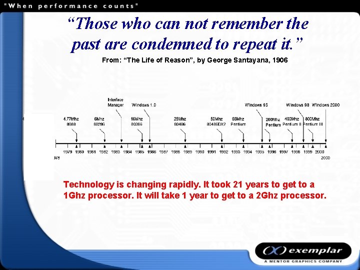
“Those who can not remember the past are condemned to repeat it. ” From: “The Life of Reason”, by George Santayana, 1906 Technology is changing rapidly. It took 21 years to get to a 1 Ghz processor. It will take 1 year to get to a 2 Ghz processor.

State-of-the-Art : Technology Process Geometries

State-of-the-Art : Gate Count (excluding memory)

State-of-the-Art : Frequency System Frequency

State-of-the-Art : Clock Domains

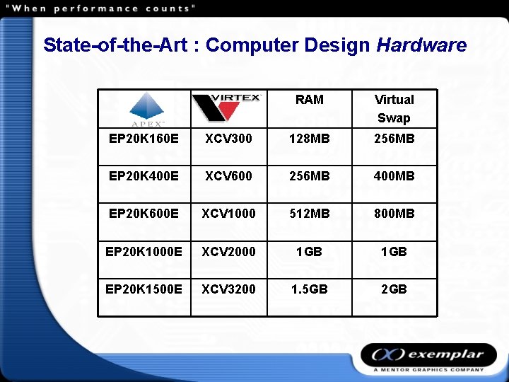
State-of-the-Art : Computer Design Hardware RAM Virtual Swap EP 20 K 160 E XCV 300 128 MB 256 MB EP 20 K 400 E XCV 600 256 MB 400 MB EP 20 K 600 E XCV 1000 512 MB 800 MB EP 20 K 1000 E XCV 2000 1 GB EP 20 K 1500 E XCV 3200 1. 5 GB 2 GB

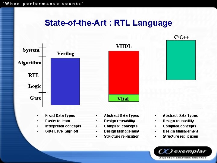
State-of-the-Art : RTL Language C/C++ System VHDL Verilog Algorithm RTL Logic Gate • • Vital Fixed Data Types Easier to learn Interpreted concepts Gate Level Sign-off • • • Abstract Data Types Design reusability Compiled concepts Design Management Structure replication

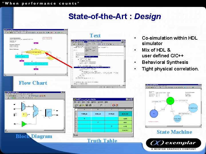
State-of-the-Art : Design Text • • Co-simulation within HDL simulator Mix of HDL & user defined C/C++ Behavioral Synthesis Tight physical correlation. Flow Chart Block Diagram State Machine Truth Table

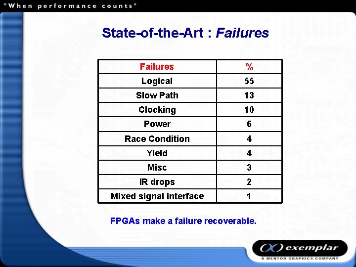
State-of-the-Art : Failures % Logical 55 Slow Path 13 Clocking 10 Power 6 Race Condition 4 Yield 4 Misc 3 IR drops 2 Mixed signal interface 1 FPGAs make a failure recoverable.

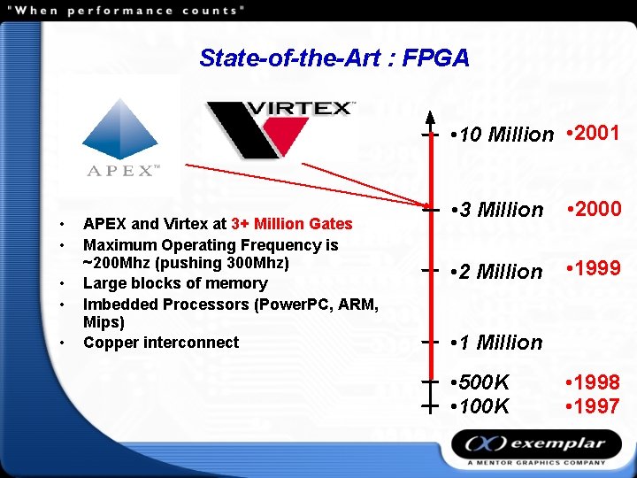
State-of-the-Art : FPGA • 10 Million • 2001 • • • APEX and Virtex at 3+ Million Gates Maximum Operating Frequency is ~200 Mhz (pushing 300 Mhz) Large blocks of memory Imbedded Processors (Power. PC, ARM, Mips) Copper interconnect • 3 Million • 2000 • 2 Million • 1999 • 1 Million • 500 K • 100 K • 1998 • 1997

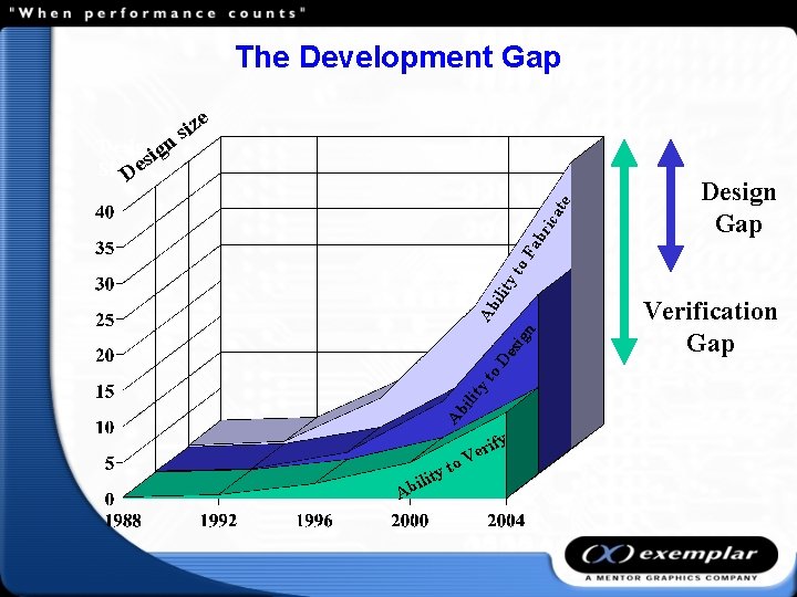
The Development Gap e te ica br to Fa Design Gap ity ign Ab il De s to ili ty Ab Designig Size. Des iz s n Ab y ilit to rify e V Verification Gap

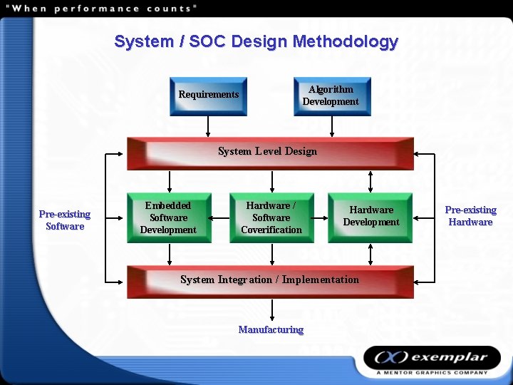
System / SOC Design Methodology Algorithm Development Requirements System Level Design Pre-existing Software Embedded Software Development Hardware / Software Coverification Hardware Development System Integration / Implementation Manufacturing Pre-existing Hardware

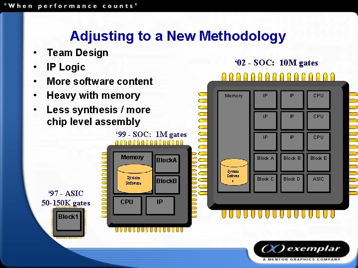
Adjusting to a New Methodology • • • Team Design IP Logic More software content Heavy with memory Less synthesis / more chip level assembly ‘ 02 - SOC: 10 M gates Memory ‘ 99 - SOC: 1 M gates Memory System Software ‘ 97 - ASIC 50 -150 K gates Block 1 CPU Block. A Block. B IP System Software Softwar e IP IP CPU Block A Block B Block E Block C Block D ASIC

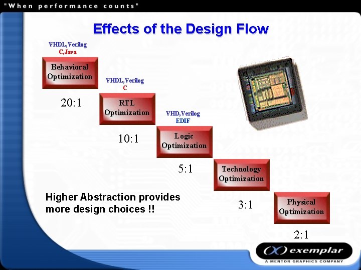
Effects of the Design Flow VHDL, Verilog C, Java Behavioral Optimization 20: 1 VHDL, Verilog C RTL Optimization 10: 1 VHD, Verilog EDIF Logic Optimization 5: 1 Higher Abstraction provides more design choices !! Technology Optimization 3: 1 Physical Optimization 2: 1

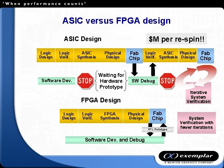
ASIC versus FPGA design $M per re-spin!! ASIC Design Logic Verif. ASIC Synthesis Physical Design Waiting for Hardware Prototype Software Dev. Fab Chip Logic ASIC Physical Verif. Synthesis Design SW Debug Iterative System Verification FPGA Design Logic Verif. FPGA Synthesis Fab Chip Physical Design Fab Chip RTL Prototype Software Dev. and Debug System Verification with fewer iterations

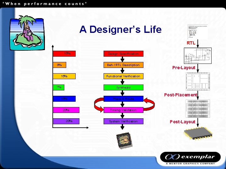
A Designer’s Life RTL 15% 8% Design Specification Beh / RTL Description 15% 7% Pre-Layout Functional Verification Synthesis 15% 20% Place & Route Post-Placement Timing Validation System Verification Post-Layout

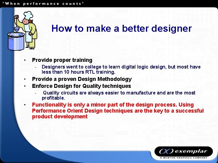
How to make a better designer • Provide proper training - • • Provide a proven Design Methodology Enforce Design for Quality techniques - • Designers went to college to learn digital logic design, but most have less than 10 hours RTL training. Quality circuits are always easier to manufacture and are the most profitable. Functionality is only a minor part of the design process. Using Performance Orient Design techniques are the key to a successful product development

Performance Oriented Design Techniques The Keys to Success • • • RTL Coding Styles Design Architecture trade-offs Design Structure Timing Optimization Physical Optimization

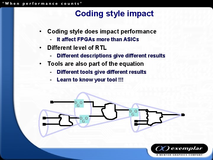
Coding style impact • Coding style does impact performance - It affect FPGAs more than ASICs • Different level of RTL - Different descriptions give different results • Tools are also part of the equation - Different tools give different results - Learn to know your tool !!! D Q G

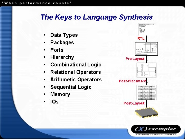
The Keys to Language Synthesis • • • Data Types Packages Ports Hierarchy Combinational Logic Relational Operators Arithmetic Operators Sequential Logic Memory IOs RTL Pre-Layout Post-Placement Post-Layout

Structuring A Design • A design should read like a book. - Table of contents : An explanation of the design structure. Logical flow from beginning to end. Chapters : Logical breaks in a design. Commentary : Comments on complex structure in the design. 99% of all designs are unintelligible to another designer !

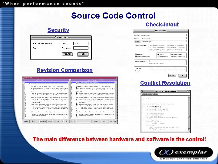
Source Code Control Security Check-in/out Revision Comparison Conflict Resolution The main difference between hardware and software is the control!

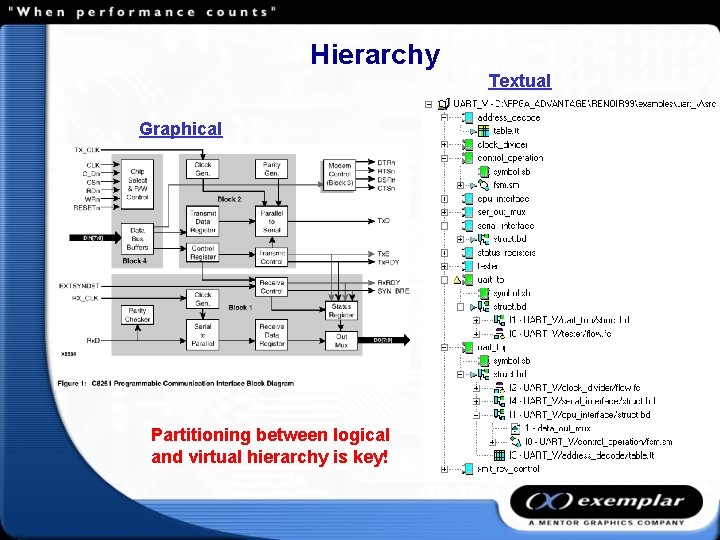
Hierarchy Textual Graphical Partitioning between logical and virtual hierarchy is key!

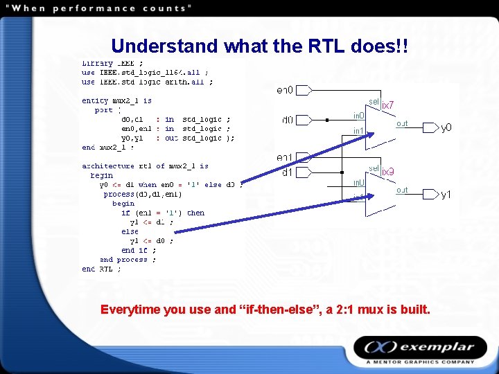
Understand what the RTL does!! Everytime you use and “if-then-else”, a 2: 1 mux is built.

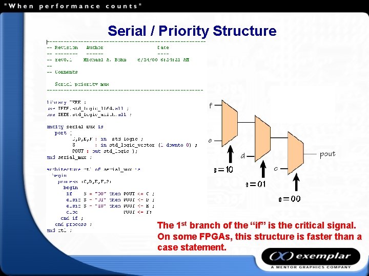
Serial / Priority Structure The 1 st branch of the “if” is the critical signal. On some FPGAs, this structure is faster than a case statement.

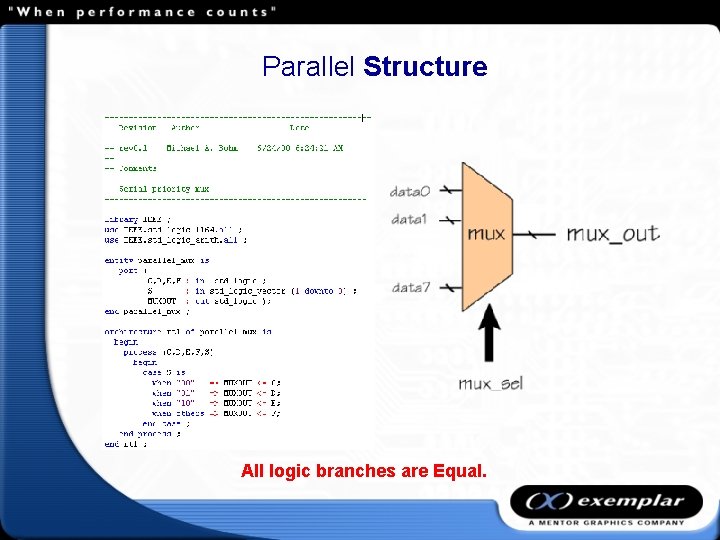
Parallel Structure All logic branches are Equal.

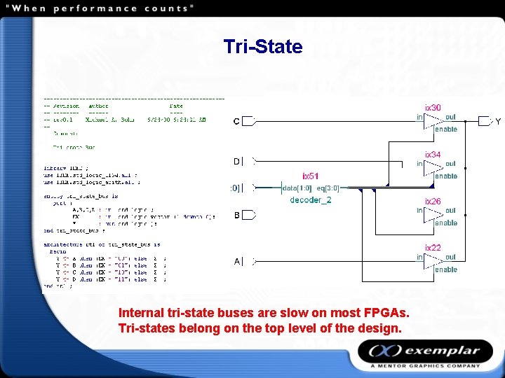
Tri-State Internal tri-state buses are slow on most FPGAs. Tri-states belong on the top level of the design.

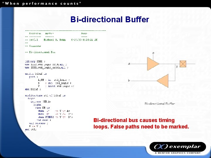
Bi-directional Buffer Bi-directional bus causes timing loops. False paths need to be marked.

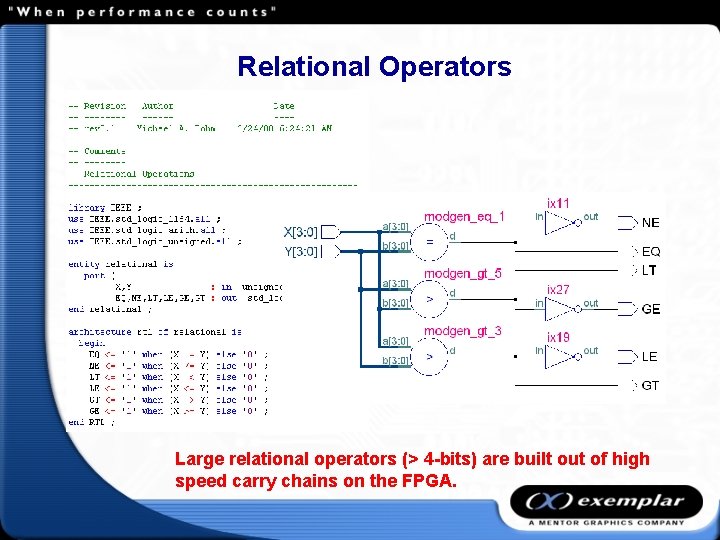
Relational Operators Large relational operators (> 4 -bits) are built out of high speed carry chains on the FPGA.

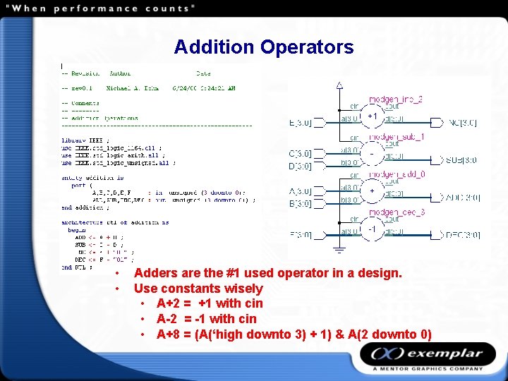
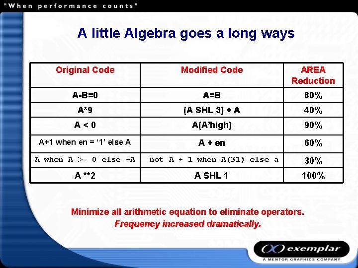
Addition Operators • • Adders are the #1 used operator in a design. Use constants wisely • A+2 = +1 with cin • A-2 = -1 with cin • A+8 = (A(‘high downto 3) + 1) & A(2 downto 0)

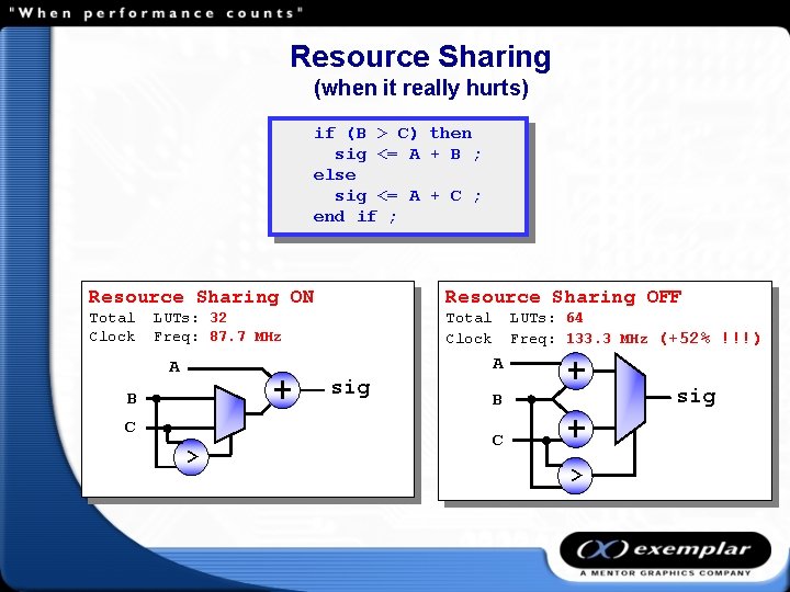
Resource Sharing (when it really hurts) if (B > C) then sig <= A + B ; else sig <= A + C ; end if ; Resource Sharing ON Resource Sharing OFF Total Clock LUTs: 32 Freq: 87. 7 MHz LUTs: 64 Freq: 133. 3 MHz (+52% !!!) A A sig B C >

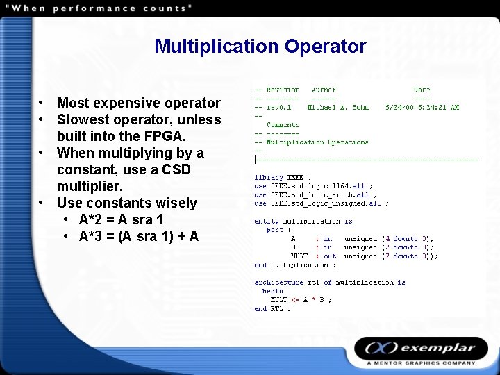
Multiplication Operator • Most expensive operator • Slowest operator, unless built into the FPGA. • When multiplying by a constant, use a CSD multiplier. • Use constants wisely • A*2 = A sra 1 • A*3 = (A sra 1) + A

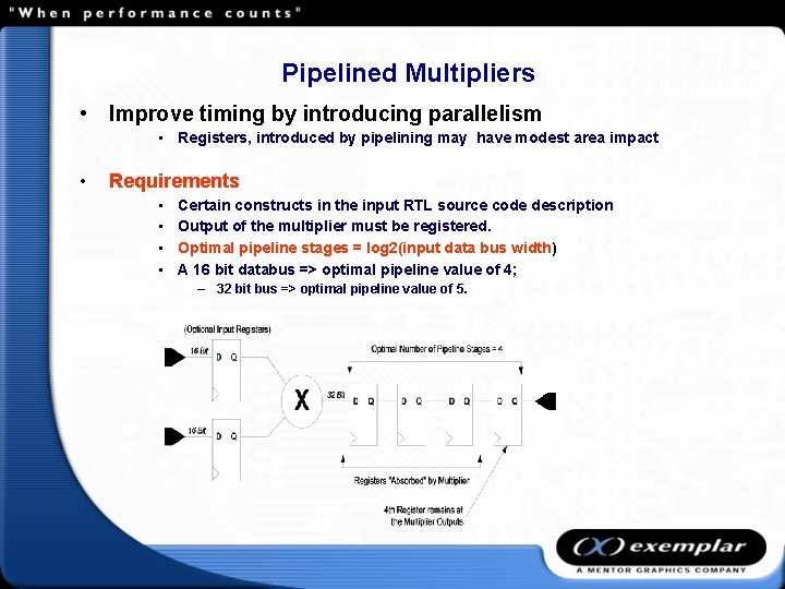
Pipelined Multipliers • Improve timing by introducing parallelism • Registers, introduced by pipelining may have modest area impact • Requirements • • Certain constructs in the input RTL source code description Output of the multiplier must be registered. Optimal pipeline stages = log 2(input data bus width) A 16 bit databus => optimal pipeline value of 4; – 32 bit bus => optimal pipeline value of 5.

A little Algebra goes a long ways Original Code Modified Code AREA Reduction A-B=0 A=B 80% A*9 (A SHL 3) + A 40% A<0 A(A’high) 90% A+1 when en = ‘ 1’ else A A + en 60% A when A >= 0 else -A A **2 not A + 1 when A(31) else a A SHL 1 30% 100% Minimize all arithmetic equation to eliminate operators. Frequency increased dramatically.

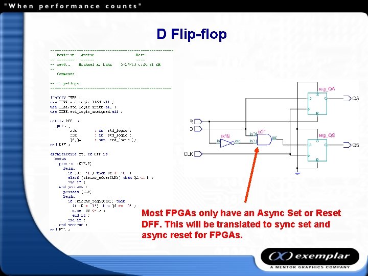
D Flip-flop Most FPGAs only have an Async Set or Reset DFF. This will be translated to sync set and async reset for FPGAs.

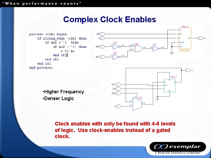
Complex Clock Enables • Higher Frequency • Denser Logic Clock enables with only be found with 4 -6 levels of logic. Use clock-enables instead of a gated clock.

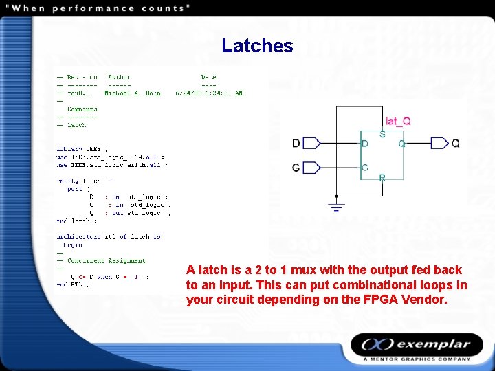
Latches A latch is a 2 to 1 mux with the output fed back to an input. This can put combinational loops in your circuit depending on the FPGA Vendor.

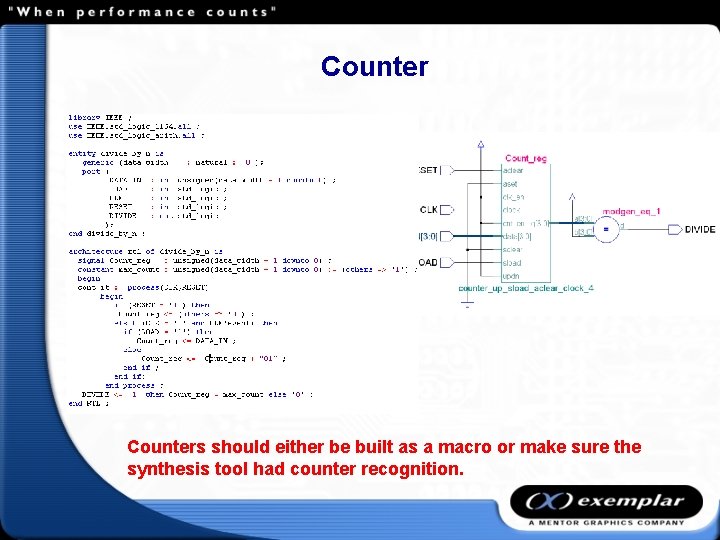
Counters should either be built as a macro or make sure the synthesis tool had counter recognition.

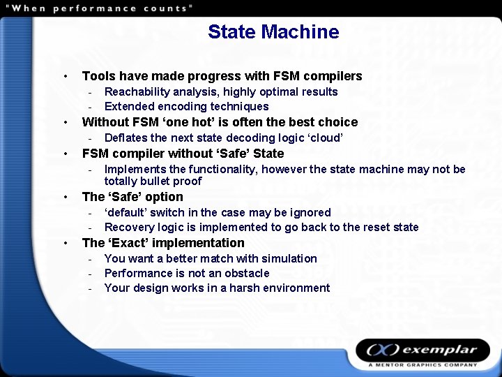
State Machine • Tools have made progress with FSM compilers - • Without FSM ‘one hot’ is often the best choice - • Implements the functionality, however the state machine may not be totally bullet proof The ‘Safe’ option - • Deflates the next state decoding logic ‘cloud’ FSM compiler without ‘Safe’ State - • Reachability analysis, highly optimal results Extended encoding techniques ‘default’ switch in the case may be ignored Recovery logic is implemented to go back to the reset state The ‘Exact’ implementation - You want a better match with simulation Performance is not an obstacle Your design works in a harsh environment

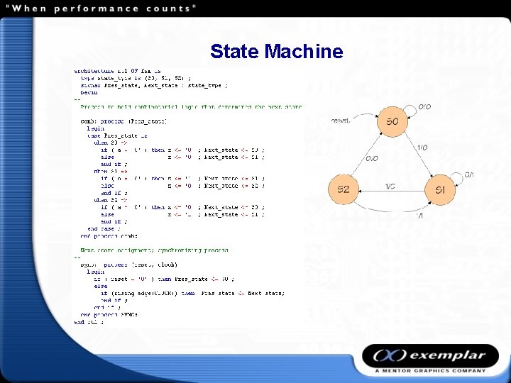
State Machine

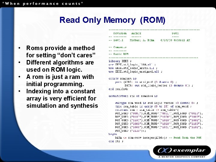
Read Only Memory (ROM) • Roms provide a method for setting “don’t cares” • Different algorithms are used on ROM logic. • A rom is just a ram with initial programming. • Indexing into a constant array is very efficient for simulation and synthesis

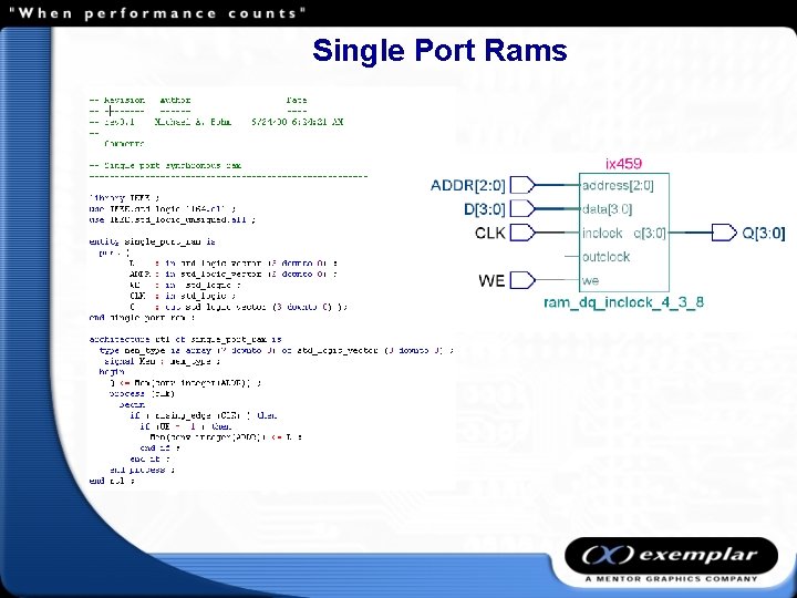
Single Port Rams

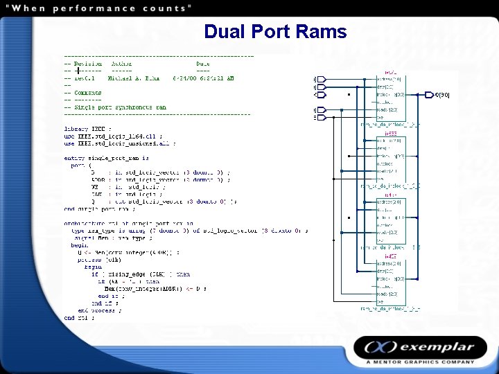
Dual Port Rams

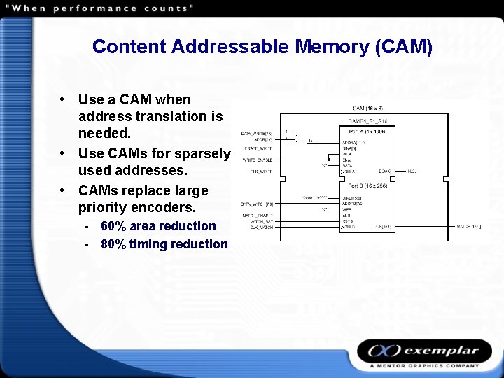
Content Addressable Memory (CAM) • Use a CAM when address translation is needed. • Use CAMs for sparsely used addresses. • CAMs replace large priority encoders. - 60% area reduction - 80% timing reduction

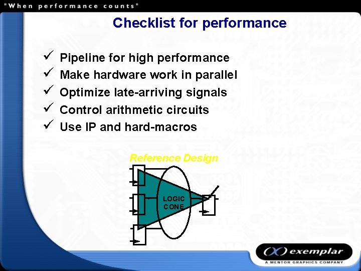
Checklist for performance ü ü ü Pipeline for high performance Make hardware work in parallel Optimize late-arriving signals Control arithmetic circuits Use IP and hard-macros Reference Design LOGIC CONE

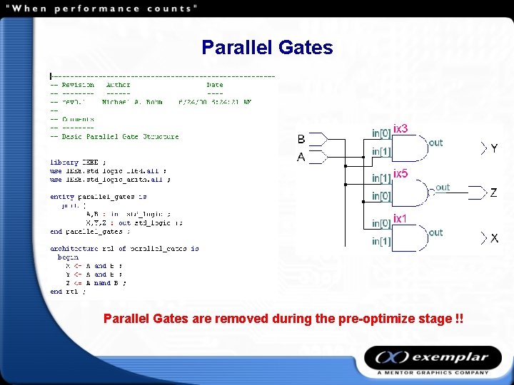
Parallel Gates are removed during the pre-optimize stage !!

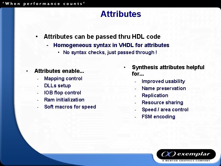
Attributes • Attributes can be passed thru HDL code - Homogeneous syntax in VHDL for attributes • No syntax checks, just passed through ! • Attributes enable. . . - Mapping control DLLs setup IOB flop control Ram initialization Soft macros for speed • Synthesis attributes helpful for. . . - Improved usability Name preservation Replication Resource sharing Speed / area control FSM encoding

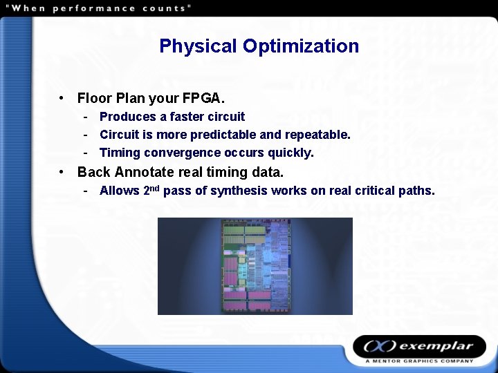
Physical Optimization • Floor Plan your FPGA. - Produces a faster circuit - Circuit is more predictable and repeatable. - Timing convergence occurs quickly. • Back Annotate real timing data. - Allows 2 nd pass of synthesis works on real critical paths.

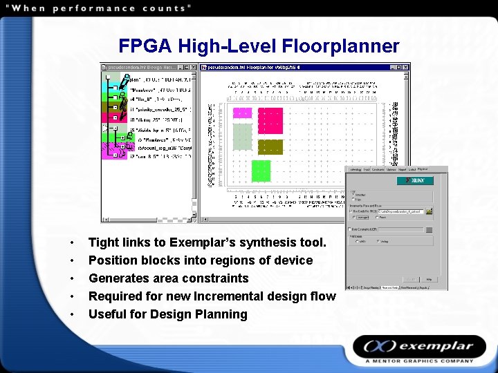
FPGA High-Level Floorplanner • • • Tight links to Exemplar’s synthesis tool. Position blocks into regions of device Generates area constraints Required for new Incremental design flow Useful for Design Planning

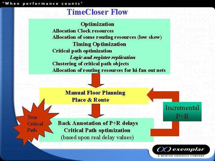
Time. Closer Flow Optimization Allocation Clock resources Allocation of some routing resources (low skew) Timing Optimization Critical path optimization Logic and register replication Clustering of critical path objects Allocation of routing resources for hi-fan out nets Manual Floor Planning Place & Route True Critical Path Back Annotation of P+R delays Critical Path optimization (based upon real delay values) Incremental P+R

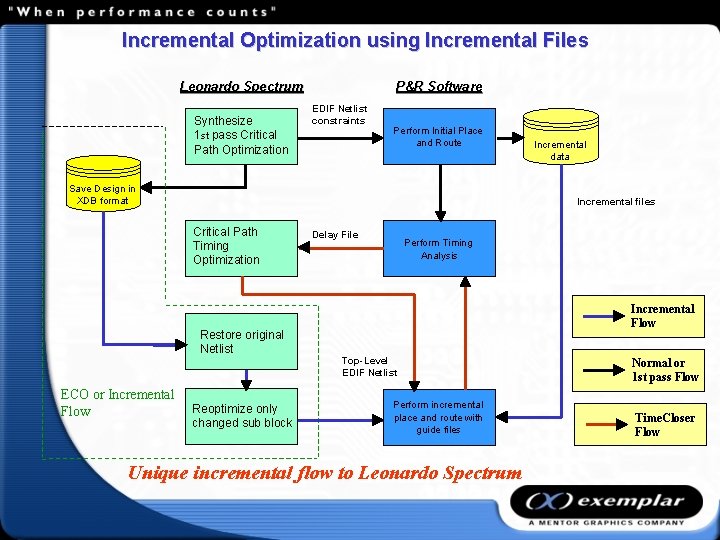
Incremental Optimization using Incremental Files Leonardo Spectrum Synthesize 1 st pass Critical Path Optimization P&R Software EDIF Netlist constraints Perform Initial Place and Route Save Design in XDB format Incremental files Critical Path Timing Optimization Restore original Netlist ECO or Incremental Flow Incremental data Reoptimize only changed sub block Delay File Perform Timing Analysis Incremental Flow Top-Level EDIF Netlist Perform incremental place and route with guide files Unique incremental flow to Leonardo Spectrum Normal or 1 st pass Flow Time. Closer Flow

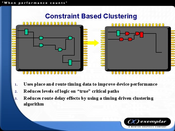
Constraint Based Clustering 1. 2. 3. Uses place and route timing data to improve device performance Reduces levels of logic on “true” critical paths Reduces route delay effects by using a timing driven clustering algorithm

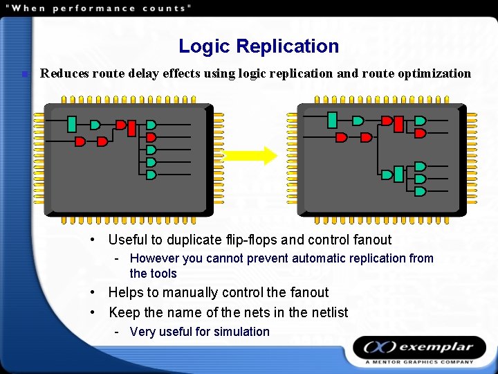
Logic Replication n Reduces route delay effects using logic replication and route optimization • Useful to duplicate flip-flops and control fanout - However you cannot prevent automatic replication from the tools • Helps to manually control the fanout • Keep the name of the nets in the netlist - Very useful for simulation

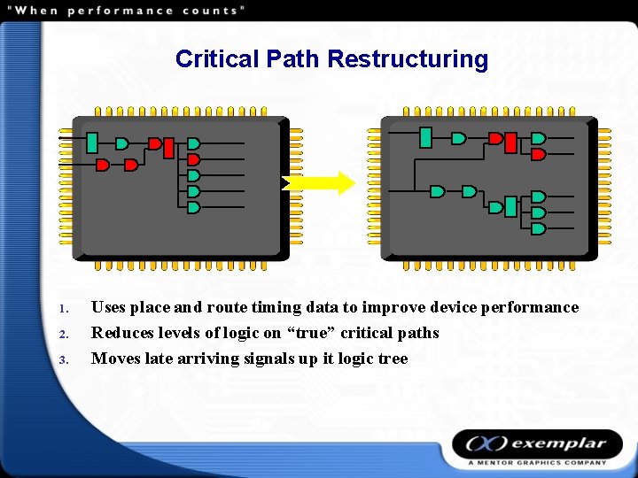
Critical Path Restructuring 1. 2. 3. Uses place and route timing data to improve device performance Reduces levels of logic on “true” critical paths Moves late arriving signals up it logic tree

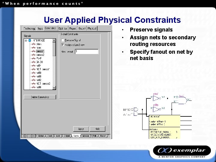
User Applied Physical Constraints • • • Preserve signals Assign nets to secondary routing resources Specify fanout on net by net basis

Design Techniques for Million Gate, High Speed FPGAs Michael A. Bohm Chief Scientist Technical Fellow Mentor Graphics