Computer Architecture Part III Decoders and Multiplexers Department
- Slides: 37

Computer Architecture Part III Decoders and Multiplexers Department of Computer Science, Faculty of Science, Chiang Mai University

Outline • • • Integrated Circuits Decoders Multiplexers Registers Memory Unit 204231: Computer Organization and Architecture 2

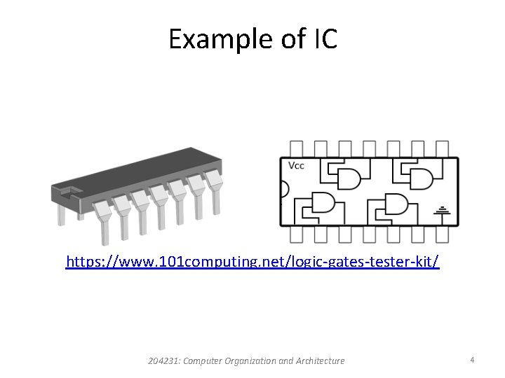
Integrated Circuits • An integrated circuit (abbreviated IC) is s mall silicon semiconductor crystal, called a chip, containing the electric components for the digital gates. 204231: Computer Organization and Architecture 3

Example of IC https: //www. 101 computing. net/logic-gates-tester-kit/ 204231: Computer Organization and Architecture 4

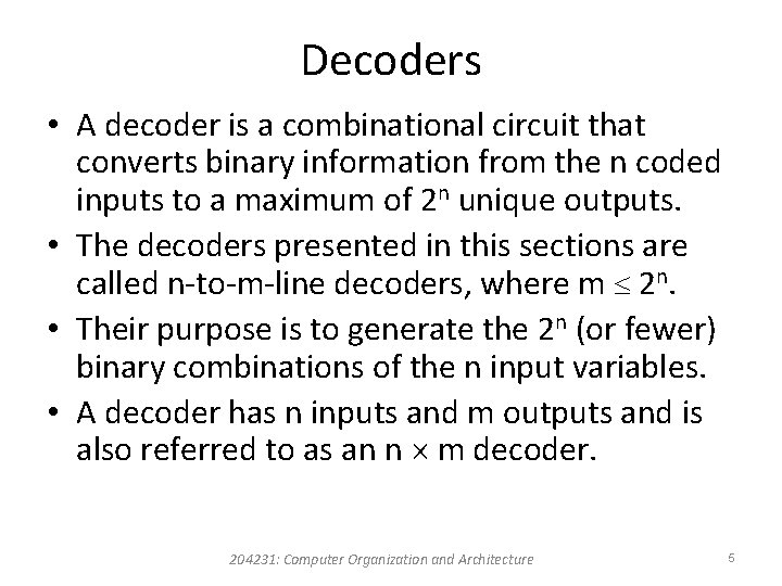
Decoders • A decoder is a combinational circuit that converts binary information from the n coded inputs to a maximum of 2 n unique outputs. • The decoders presented in this sections are called n-to-m-line decoders, where m 2 n. • Their purpose is to generate the 2 n (or fewer) binary combinations of the n input variables. • A decoder has n inputs and m outputs and is also referred to as an n m decoder. 204231: Computer Organization and Architecture 5

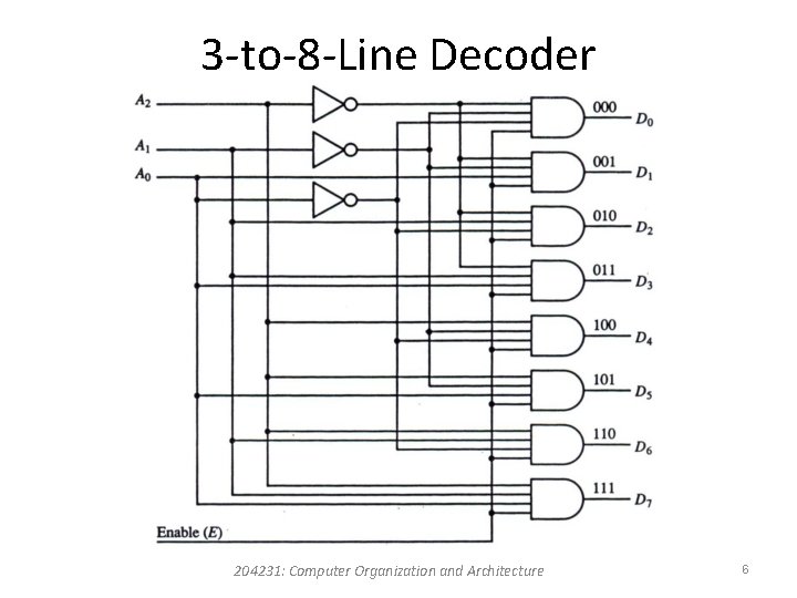
3 -to-8 -Line Decoder 204231: Computer Organization and Architecture 6

3 -to-8 -Line Decoder • The three data inputs, A 0, A 1, and A 2, are decoded into eight outputs, each output represent one of the combinations of the three binary input variables. • A particular application of this decoder is a binaryto-octal conversion. • Commercial decoders include one or more enable inputs to control the operation of the circuit. • The decoder is enabled when E is equal to 1 and disabled when E is equal to 0. 204231: Computer Organization and Architecture 7

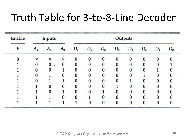
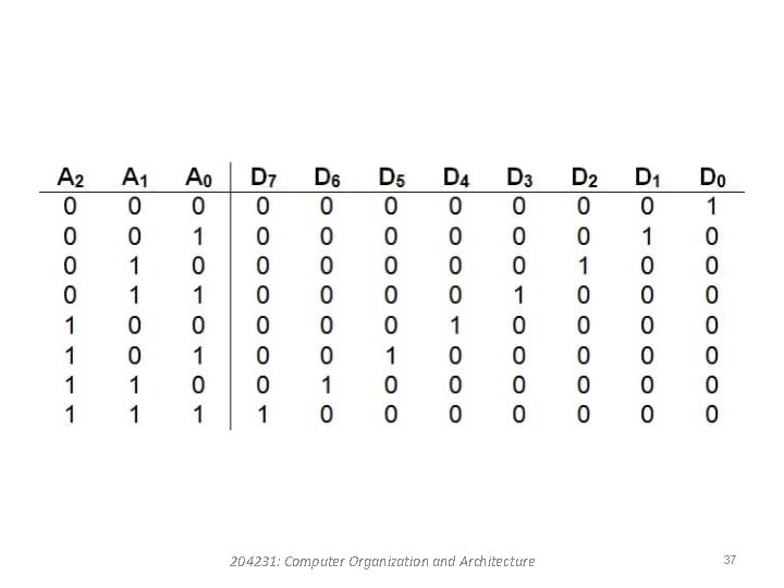
Truth Table for 3 -to-8 -Line Decoder • When the enable input E is equal to 0, all the outputs are equal to 0 regardless of the values of the othere data inputs. • The there x’s in the table designate don’t-care conditions. • When the enable input is equal to 1, the decoder operates in a normal fashion. 204231: Computer Organization and Architecture 8

Truth Table for 3 -to-8 -Line Decoder • For each possible input combination, there are seven outputs that are equal to 0 and only one that is equal to 1. • The output variable whose value is equal to 1 represents the octal number equivalent of the binary number that is available in the input data lines. 204231: Computer Organization and Architecture 9

Truth Table for 3 -to-8 -Line Decoder 204231: Computer Organization and Architecture 10

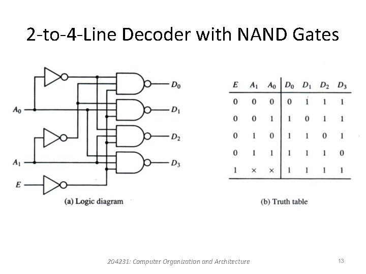
NAND Gate Decoder • Some decoders are constructed with NAND instead of AND gates. • The decoder is enabled when E is equal to 0. • As indicated by the truth table, only one output is equal to 0 at any give time; the other three outputs are equal to 1. 204231: Computer Organization and Architecture 11

NAND Gate Decoder • The output whose value is equal to 0 represents the equivalent binary number in inputs A 1 and A 0. • The circuit is disabled when E is equal to 1, regardless of the values of the other two inputs. 204231: Computer Organization and Architecture 12

2 -to-4 -Line Decoder with NAND Gates 204231: Computer Organization and Architecture 13

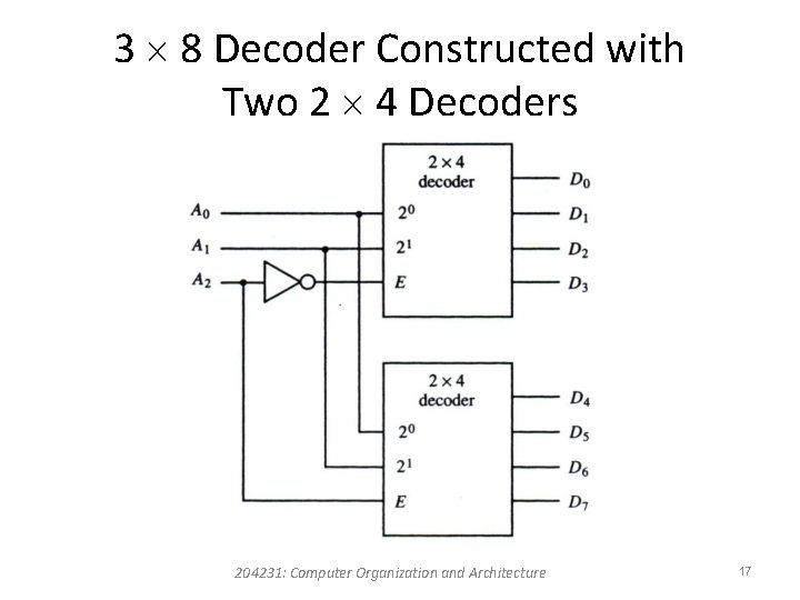
Decoder Expansion • Two 2 -to-4 -line decoders are combined to achieve a 3 -to-8 -line decoder. • The two least significant bits of the input are connected to both decoders. • The most significant bit is connected to the enable input of one decoder and through an inverter to the enable input of the other decoder. 204231: Computer Organization and Architecture 14

Decoder Expansion • It is assumed that each decoder is enabled when its E input is equal to 1. • When E is equal to 0, the decoder is disabled and all its outputs are in the 0 level. • When A 2 = 0, the upper decoder is enabled and the lower is disabled. 204231: Computer Organization and Architecture 15

Decoder Expansion • The outputs of the upper decoder generate outputs D 0 through D 3, depending on the values of A 1 and A 0. • When A 2 = 1, the lower decoder is enabled and the upper is disabled. • The lower decoder output generates the binary equivalent D 4 through D 7. 204231: Computer Organization and Architecture 16

3 8 Decoder Constructed with Two 2 4 Decoders 204231: Computer Organization and Architecture 17

Multiplexers • A multiplexer is a combinational circuit that receives binary information from one of 2 n input data lines and directs it to a single output line. • The selection of a particular input data line for the output is determined by a set of selection inputs. • A 2 n-to-1 multiplexer has 2 n input data lines and n input selection lines whose bit combinations determine which input data are selected for the output. 204231: Computer Organization and Architecture 18

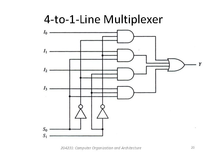
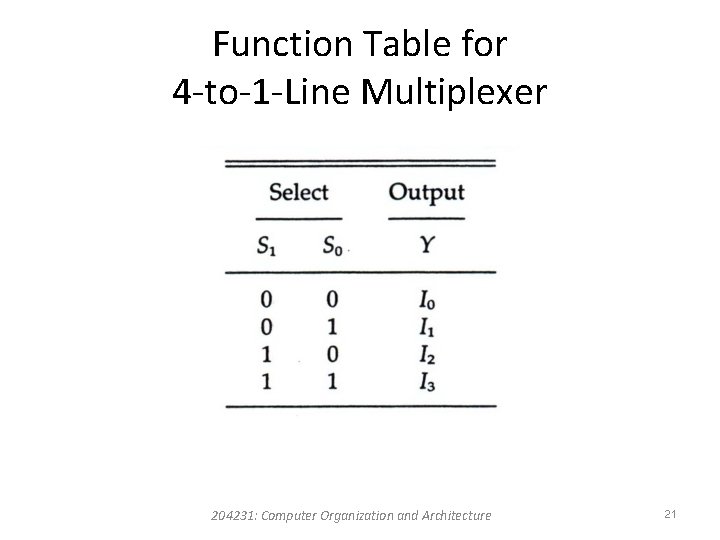
4 -to-1 -Line Multiplexer • Each of the four data inputs I 0 through I 3 is applied to one input of and AND gate. • The two selection inputs S 1 and S 0 are decoded to select a particular AND gate. • The outputs of the AND gates are applied to a single OR gate to provide the single output. • A more convenient way to describe the operation of multiplexers is by means of a function table. 204231: Computer Organization and Architecture 19

4 -to-1 -Line Multiplexer 204231: Computer Organization and Architecture 20

Function Table for 4 -to-1 -Line Multiplexer 204231: Computer Organization and Architecture 21

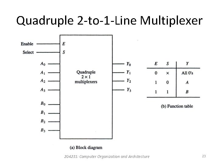
Quadruple 2 -to-1 -Line Multiplexer • One or more multiplexers can be enclosed with in a single integrated circuit. • The selection and the enable inputs in multiple -unit construction are usually common to all multiplexers. • Quadruple 2 -to-1 -line multiplexer has four multiplexers. 204231: Computer Organization and Architecture 22

Quadruple 2 -to-1 -Line Multiplexer 204231: Computer Organization and Architecture 23

Registers • In its broadest definition, a register consists of a group of flip-flops and gates that effect their transition. • The flip-flops hold the binary information and the gates control when and how new information is transferred into the register. 204231: Computer Organization and Architecture 24

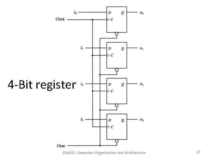
4 -Bit Register • The register is constructed with four D flipflops. • The common clock input triggers all flip-flops on the rising edge of each pulse, and the binary data available at the four inputs are transferred into the 4 -bit register. • The four outputs can be sampled at any time to obtain the binary information stored in the register. 204231: Computer Organization and Architecture 25

4 -Bit Register • The clear input goes to a special terminal in each flip-flop. • When this input goes to 0, all flip-flops are reset asynchronously. • The clear input is useful for clearing the register to all 0’s prior to its clocked operation. 204231: Computer Organization and Architecture 26

4 -Bit register 204231: Computer Organization and Architecture 27

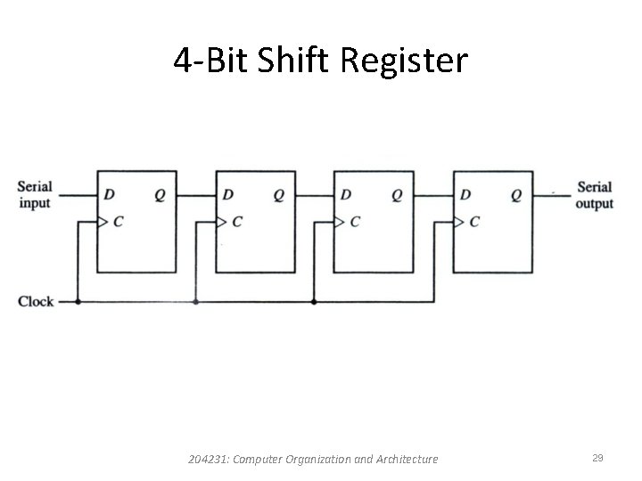
Shift Registers • A register capable of shifting its binary information in one or both directions is called a shift register. • The logical configuration of a shift register consists of a chain of flip-flops in cascade, with the output of one flip-flop connected to the input of the next flip-flop. • All flip-flop receive common clock pulses that initiate the shift from one stage to the next. 204231: Computer Organization and Architecture 28

4 -Bit Shift Register 204231: Computer Organization and Architecture 29

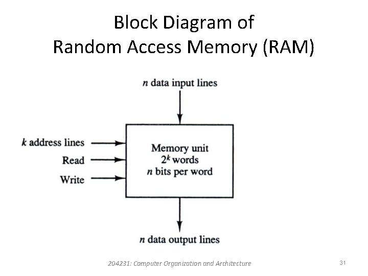
Random-Access Memory • The n data input lines provide the information to be stored in memory, and the n data output lines supply the information coming out of memory. • The k address lines provide a binary number of k bits that specify a particular word chosen among the 2 k available inside the memory. • The two control inputs specify the direction of transfer desired. 204231: Computer Organization and Architecture 30

Block Diagram of Random Access Memory (RAM) 204231: Computer Organization and Architecture 31

Transferring a New Word to be Stored into Memory 1. Apply the binary address of the desired word into the address lines. 2. Apply the data bits that must be stored in memory into the data input lines. 3. Activate the write input. 204231: Computer Organization and Architecture 32

Transferring a Stored Word Out of Memory 1. Apply the binary address of the desired word into the address lines. 2. Activate the read input. 204231: Computer Organization and Architecture 33

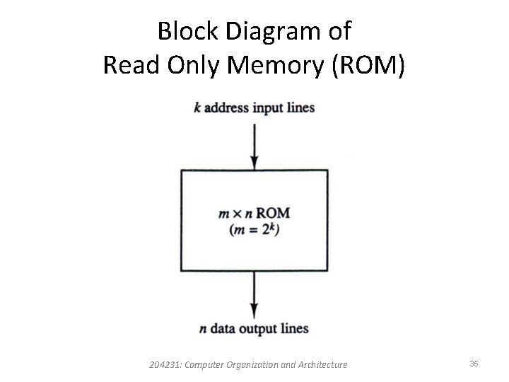
Read-Only Memory • An m x n ROM is an array of binary cells organized into m words of n bits each. • A ROM has k address input lines to select one of 2 k = m words of memory, and n output lines, one for each bit of the word. • The ROM does not need a read-control line since at any given time, the output lines automatically provide the n bits of the word selected by the address value. 204231: Computer Organization and Architecture 34

Block Diagram of Read Only Memory (ROM) 204231: Computer Organization and Architecture 35

Reference • M. Moris Mano, Computer System Architecture, 3 rd ed. NJ: Prentice Hall, 1992. 204231: Computer Organization and Architecture 36

204231: Computer Organization and Architecture 37