Microcontrollers What is a Microcontroller MiniComputer Microprocessor The

 Control")


 { TRISA 0 =")


")


")


- Slides: 46
Microcontrollers
What is a Microcontroller? Mini-Computer ◦ Microprocessor The Brains Arithmetic Logic Unit (ALU) Control Unit Program/ Data Storage Peripherals (Input/Output) Low-Cost
Why Important? Embedded Inside: ◦ ◦ ◦ Automotive systems Airplanes Toys Medical Devices Furniture Billions of units
Available u. C in Bangladesh AT 89 C 51 AT 89 C 52 AT 89 S 51 AT 89 S 52 ATMEGA-8 AT 89 C 2051 AT 89 C 4051 AT 89 C 55 WD AT 89 S 8252 AT 90 S 2313 AT 90 S 8515 AT 90 S 8535 ATMEGA-16 ATMEGA-32 ATMEGA-64 ATMEGA-88 ATTINY-13 ATTINY-15 ATTINY-26 AT 89 C 51 ED 2 AT 89 C 51 RD 2 AT 91 RM 9200 AT 91 SAM 256 ATMEGA-128 ATMEGA-162 W 78 E 052 B 40 DL
Available u. C in Bangladesh PIC 16 F 72 PIC 16 F 74 PIC 16 F 77 PIC 10 F 200 PIC 12 F 629 PIC 16 C 54 C PIC 16 C 65 B PIC 16 F 676 PIC 18 F 452 PIC 16 F 628 A PIC 16 F 873 A PIC 16 F 877 A PIC 18 F 4550 PIC 16 F 73 PIC 16 F 76 PIC 16 F 88 PIC 12 F 508 PIC 12 F 675 PIC 16 C 57 C PIC 16 C 923 PIC 16 F 84 A PIC 16 C 622 A PIC 16 F 648 A PIC 16 F 876 A PIC 18 F 2550
PIC 16 F 877 A 40 -Pin Enhanced Flash, 8 -Bit CMOS Microcontrollers with Nano Watt Technology Wide operating voltage range (2. 0 V-5. 5 V) 33 I/O pins Two 8 -bit Timer, One 16 -bit Timer 8 -channel, 10 -bit ADC Programmable Serial USART Internal Calibrated RC Oscillator DC – 20 MHz oscillator/clock input Software selectable frequency range of 8 MHz to 32 k. Hz
Pin Diagram
What do I need to start? To start C programming language on Microchip PIC Microcontroller you need these following tools: Down load the latest Mikro. C and Install it The PIC 16 F 877 A datasheet Microchip Programmer. Trainer Board
I/O Port For Port A, B, C, D, E there are control bytes TRISx. Setting a TRISx bit (= 1) will make the corresponding PORTx pin an input Clearing a TRISx bit (= 0) will make the corresponding PORTx pin an output
TRISA and PORTA
TRISB and PORTB
TRISC and PORTC
TRISD and PORTD
TRISE and PORTE
Write the first code and simulate #include<pic. h> void main() { TRISA 0 = 1; TRISC = 0; ADCON 1=0 b 00000110; while (1) { if(PORTA == 0) { PORTC = 0; } else if (PORTA 0 == 1) { PORTC = 1; } } } // main function // declare RA 0 pin as input // declare POART C as output //declare RA 0 pin as digital // working loop
Open ISIS Professional from Proteus Program
Draw the circuit
Specify HEX file to Microcontroller
Simulate the Circuit with Microcontroller Program
Output current caution Ensure that the output current <20 m. A Maximum output current sunk by any I/O pin. . . . . . . 25 m. A Maximum output current sourced by any I/O pin. . . . . . 25 m. A Maximum current sunk by PORTA, PORTB and PORTC (combined). . . . 200 m. A Maximum current sourced PORTA, PORTB and PORTC (combined). . . . 200 m. A
Input
Input Arrangement For hardware side, use 1 uf-10 uf Capacitor across the push button if the input source is a push button. Solve the de-bouncing problem by programming accordingly.
Class work Write a program that ◦ takes input from RC 0 and RC 1 ◦ Output LED at RC 2 is light while any of the input is high ◦ Output LED as RC 3 is light while both of the inputs are high Simulate it and run it to the Microcontroller
◦ TRISC 0=1; // defined as input ◦ TRISC 1=1; // defined as input ◦ TRISC 2=0; // defined as output ◦ TRISC 3=0; // defined as output While(1){ RC 2=RC 0 | RC 1; RC 3= RC 0 &RC 1; }
Analog to Digital Converter 10 -bit Resolution 13 - 260 μs Conversion Time 8 Multiplexed Single Ended Input Channels 0 - VCC ADC Input Voltage Range Selectable 2. 56 V ADC Reference Voltage
Analog to Digital Converter 10 -bit Resolution
Analog to Digital Converter 8 Multiplexed Single Ended Input Channels
Analog to Digital Converter 0 - VCC ADC Input Voltage Range
Analog to Digital Converter Selectable 2. 56 V ADC Reference Voltage
A general diagram of ADC
Block Diagram
ADC Block Diagram(PIC 16 F 690)
Related Pins
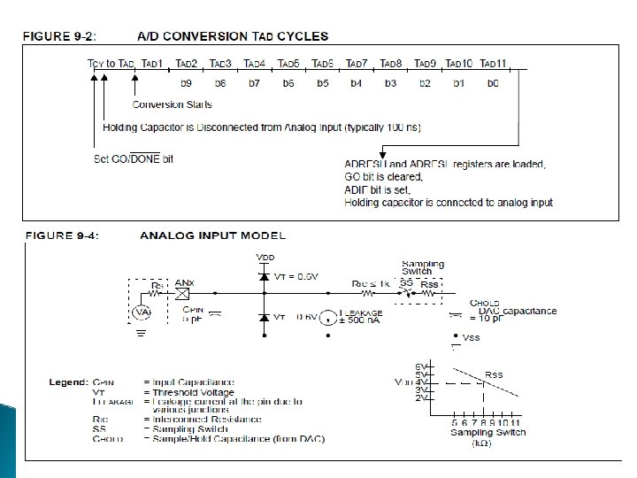
Configuration Sequence Enable ADC Analog input channel declaration Channel Selection Clock Selection Start a conversion Wait until the conversion finishes When the conversion is done, read the 8 bit LSB from ADRESL and 2 bit MSB from ADRESH byte. Concatenate them to get 10 bit conversion
Configuration Bytes There are the registers available to control the functionality of the A/D module: 1. ADON=1 2. ADCS 2, 1, 0 3. CHS 2, 1, 0
Enabling ADC
Analog input channel declaration Set the corresponding TRISx bits to ‘ 1’ to set the pin output driver to its high-impedance state. Likewise, set the corresponding ANSx bit to disable the digital input buffer.
ADC
ADC clock source
CONVERSION OUTPUT The A/D conversion can be supplied in two formats: Left or right justified. The ADFM bit (ADCON 0<7>) controls the output format.
VOLTAGE REFERENCE There are two options for the voltage reference to the A/D converter: either VDD is used or an analog voltage applied to VREF is used. The VCFG bit (ADCON 0<6>)controls the voltage reference selection. If VCFG is set, then the voltage on the VREF pin is the reference; otherwise, VDD is the reference.
Voltage Reference(not applicable)
CONVERSION CLOCK The source of the conversion clock is software selectable via the ADCS bits (ADCON 1<6: 4>).
STARTING A CONVERSION The A/D conversion is initiated by setting the GO/DONE bit (ADCON 0<1>). When the conversion is complete, the A/D module: Clears the GO/DONE bit
ADC