Memory Overview Memory stores the program running and



- Slides: 57

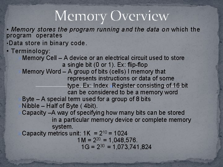
Memory Overview • Memory stores the program running and the data on which the program operates • Data store in binary code. • Terminology: ØMemory Cell – A device or an electrical circuit used to store a single bit (0 or 1). Ex: flip-flop ØMemory Word – A group of bits (cells) I memory that represents instructions or data of some type. Ex: Index Register consisting of 16 bit can be considered to be a memory word ØByte – A special term used for a group of 8 bits ØNibble – Half of Byte ( 4 bit). ØCapacity –A way of specifying how many bits can be stored in a particular memory device or complete memory system. ØCapacity metrics unit: 1 K = 210 = 1024. 1 M = 220 = 1, 048, 576. 1 G = 2 30 = 1, 073, 741, 824


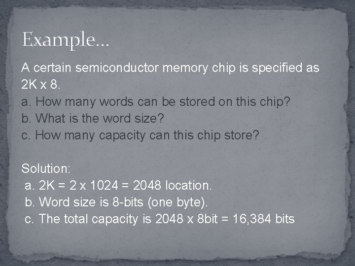
Example… A certain semiconductor memory chip is specified as 2 K x 8. a. How many words can be stored on this chip? b. What is the word size? c. How many capacity can this chip store? Solution: a. 2 K = 2 x 1024 = 2048 location. b. Word size is 8 -bits (one byte). c. The total capacity is 2048 x 8 bit = 16, 384 bits

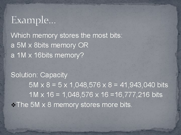
Example… Which memory stores the most bits: a 5 M x 8 bits memory OR a 1 M x 16 bits memory? Solution: Capacity 5 M x 8 = 5 x 1, 048, 576 x 8 = 41, 943, 040 bits 1 M x 16 = 1, 048, 576 x 16 =16, 777, 216 bits v. The 5 M x 8 memory stores more bits.

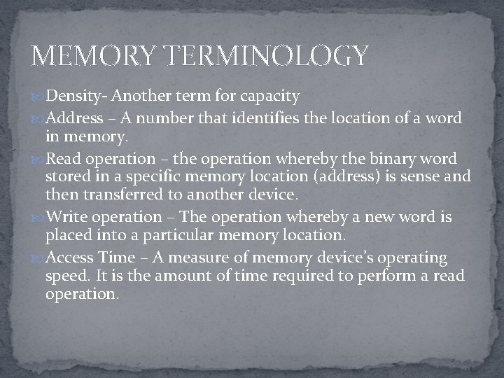
MEMORY TERMINOLOGY Density- Another term for capacity Address – A number that identifies the location of a word in memory. Read operation – the operation whereby the binary word stored in a specific memory location (address) is sense and then transferred to another device. Write operation – The operation whereby a new word is placed into a particular memory location. Access Time – A measure of memory device’s operating speed. It is the amount of time required to perform a read operation.

MEMORY TERMINOLOGY Density- Another term for capacity Address – A number that identifies the location of a word in memory. Read operation – the operation whereby the binary word stored in a specific memory location (address) is sense and then transferred to another device. Write operation – The operation whereby a new word is placed into a particular memory location. Access Time – A measure of memory device’s operating speed. It is the amount of time required to perform a read operation.

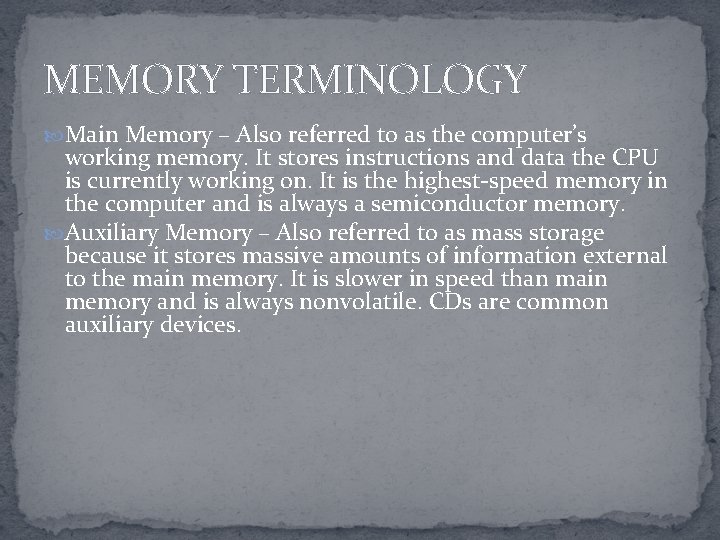
MEMORY TERMINOLOGY Main Memory – Also referred to as the computer’s working memory. It stores instructions and data the CPU is currently working on. It is the highest-speed memory in the computer and is always a semiconductor memory. Auxiliary Memory – Also referred to as mass storage because it stores massive amounts of information external to the main memory. It is slower in speed than main memory and is always nonvolatile. CDs are common auxiliary devices.

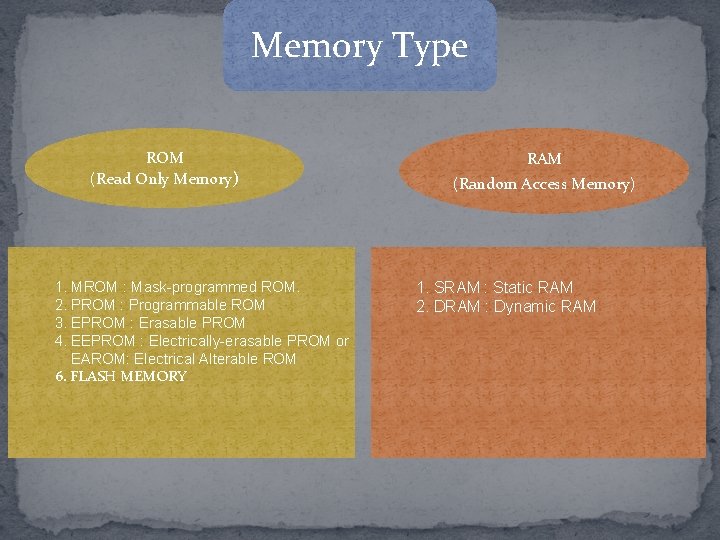
Memory Type ROM (Read Only Memory) 1. MROM : Mask-programmed ROM. 2. PROM : Programmable ROM 3. EPROM : Erasable PROM 4. EEPROM : Electrically-erasable PROM or EAROM: Electrical Alterable ROM 6. FLASH MEMORY RAM (Random Access Memory) 1. SRAM : Static RAM 2. DRAM : Dynamic RAM

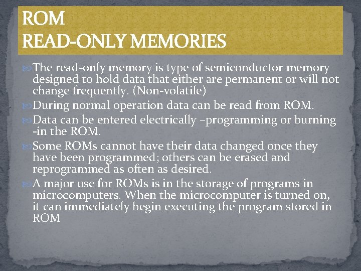
ROM READ-ONLY MEMORIES The read-only memory is type of semiconductor memory designed to hold data that either are permanent or will not change frequently. (Non-volatile) During normal operation data can be read from ROM. Data can be entered electrically –programming or burning -in the ROM. Some ROMs cannot have their data changed once they have been programmed; others can be erased and reprogrammed as often as desired. A major use for ROMs is in the storage of programs in microcomputers. When the microcomputer is turned on, it can immediately begin executing the program stored in ROM

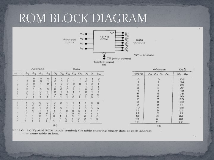
ROM BLOCK DIAGRAM

ROM BLOCK DIAGRAM Has 3 sets of signals: address inputs, control inputs, and data outputs. Store 16 words because it has 2^4=16 possible addresses, and each word contains 8 -bit because there are 8 data outputs. This is a 16 x 8 ROM. The most common numbers of data outputs for ROMs are 4, 8, 16 bits with 8 -bit word being the most common. Control input CS-Chip Select – an enable input that enables or disabled the ROM outputs Many ROMs have two or more control inputs that must be active in order to enable the data outputs so that data can be read from the selected address.

ROM BLOCK DIAGRAM CS input shown in figure is active-LOW; therefore, it must be in the LOW state to enable the ROM data to appear at the data outputs Notice that there are no R/W input because the ROM cannot be written into during normal operation.

THE READ OPERATION 16 different data words are stored at the 16 different address locations. In order to read a data word from ROM, we need to do 2 things : Apply the appropriate address inputs Activate the control inputs. Ex: if we want to read the data stored at location 0111 of the ROM, we must apply A 3 A 2 A 1 A 0=0111 to the address inputs and then apply a LOW to CS. The address inputs will be decoded inside the ROM to select the correct data word, 11101101, that will appear at outputs D 7 to D 0. If CS is kept HIGH the ROM outputs will be disabled and will be in the Hi-Z state.

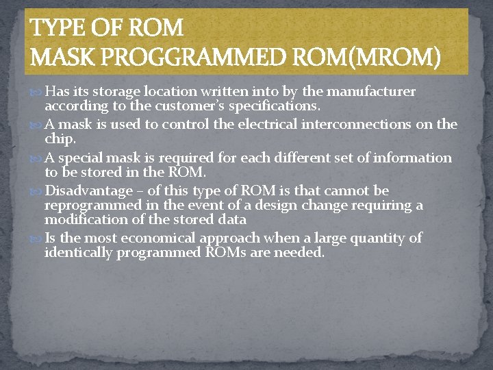
TYPE OF ROM MASK PROGGRAMMED ROM(MROM) Has its storage location written into by the manufacturer according to the customer’s specifications. A mask is used to control the electrical interconnections on the chip. A special mask is required for each different set of information to be stored in the ROM. Disadvantage – of this type of ROM is that cannot be reprogrammed in the event of a design change requiring a modification of the stored data Is the most economical approach when a large quantity of identically programmed ROMs are needed.

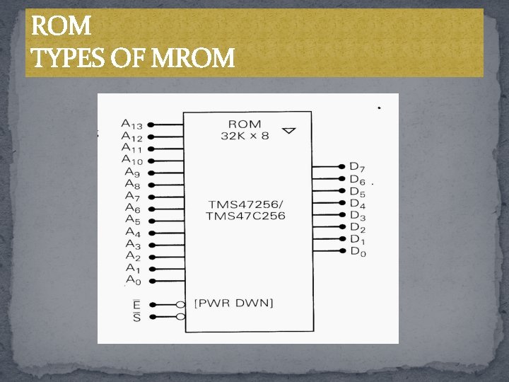
ROM TYPES OF MROM

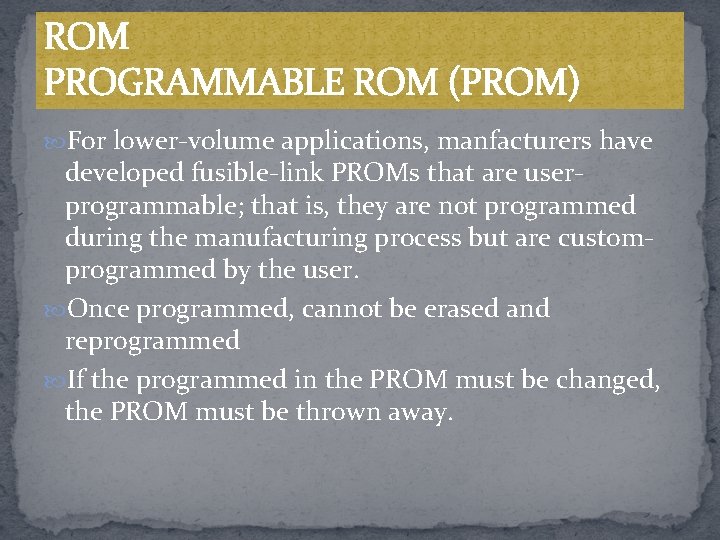
ROM PROGRAMMABLE ROM (PROM) For lower-volume applications, manfacturers have developed fusible-link PROMs that are userprogrammable; that is, they are not programmed during the manufacturing process but are customprogrammed by the user. Once programmed, cannot be erased and reprogrammed If the programmed in the PROM must be changed, the PROM must be thrown away.

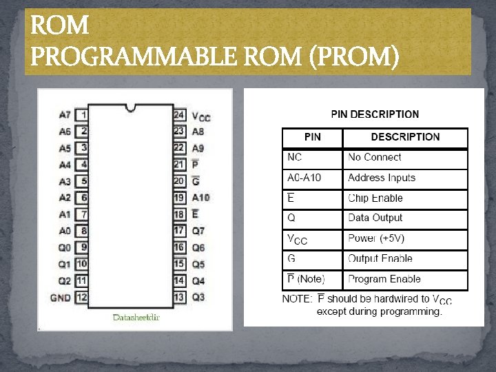
ROM PROGRAMMABLE ROM (PROM)

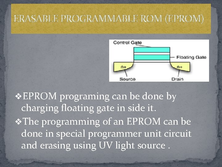
ERASABLE PROGRAMMABLE ROM (EPROM) EPROM samb. v. EPROM programing can be done by charging floating gate in side it. v. The programming of an EPROM can be done in special programmer unit circuit and erasing using UV light source.

ERASABLE PROGRAMMABLE ROM (EPROM) Can be programmed by the user and can be erased and reprogrammed as often as desired. Nonvolatile memory that will hold its stored data indefinitely The programming process is usually performed by a special programming circuit that is separate from he circuit in which the EPROM will eventually be working. EPROMs are available in a wide range of capacities and access times; devices with a capacity of 512 K x 8 and can access time of 20 ns are commonplace

ROM ERASABLE PROGRAMMABLE ROM (EPROM) Disadvantages: 1. 2. 3. They must be removed from their circuit to be erased and reprogrammed The erase operation erases the entire chip-there is no way to select only certain addresses to be erased The erase and reprogramming process can typically take 20 minutes or more.

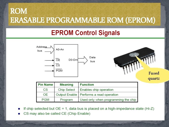
ROM ERASABLE PROGRAMMABLE ROM (EPROM) Fused quartz

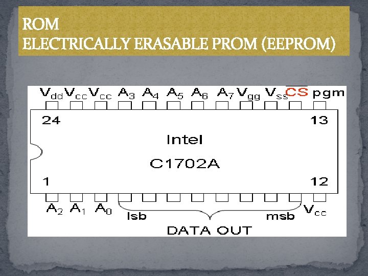
ROM ELECTRICALLY ERASABLE PROM (EEPROM) v The disadvantages of the EPROM were overcome by the development of the electrically erasable PROM (EEPROM) as an improvement over the EPROM. �The erasing and programming of an EPROM can be done in circuit ( without UV light source or a special programmer unit) �Advantages: ability to erase and rewrite individual bytes (8 -bit words) in the memory array electrically. �During a write operation, internal circuitry automatically erases all of the cells at an address location prior to writing in the new data. This byte eras ability makes it much easier to make changes in the data stored in an EEPROM

ROM ELECTRICALLY ERASABLE PROM (EEPROM)

ROM FLASH MEMORY From EEPROM to Flash memory cell, is like the simple singe- transistor EPROM cell, being only slightly larger. Allows electrical erasability but can be built with much higher densities than EEPROMs. The cost of flash memory is considerably less than for EEPROM Rapid erase and write times. Use bulk erase operation in which all cells on the chip are erase simultaneously This bulk erase process typically requires hundreds of milliseconds compares to 20 minutes for UV EPROMs

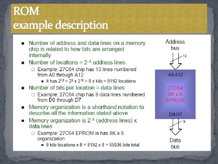
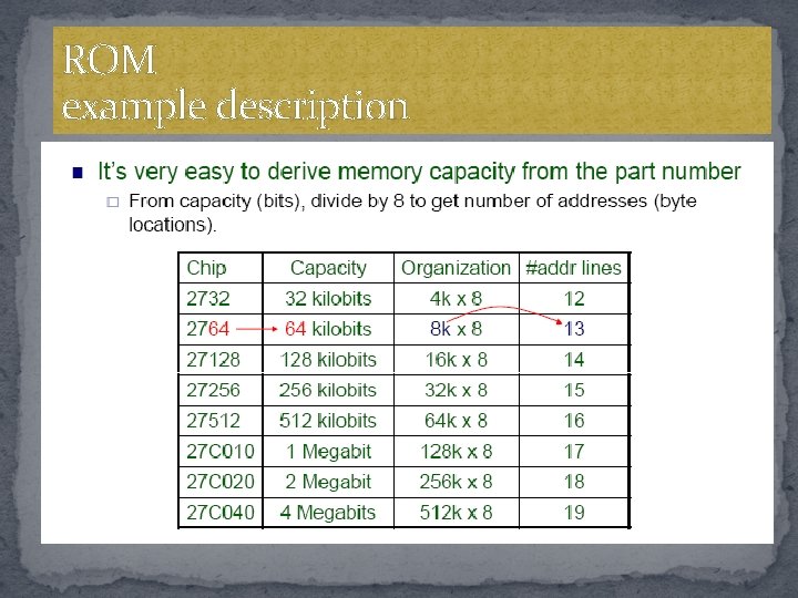
ROM example description

ROM example description

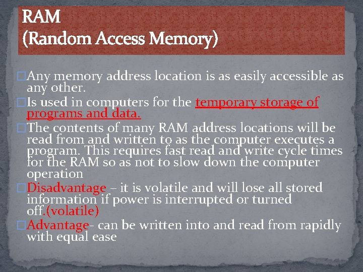
RAM (Random Access Memory) �Any memory address location is as easily accessible as any other. �Is used in computers for the temporary storage of programs and data. �The contents of many RAM address locations will be read from and written to as the computer executes a program. This requires fast read and write cycle times for the RAM so as not to slow down the computer operation �Disadvantage – it is volatile and will lose all stored information if power is interrupted or turned off. (volatile) �Advantage- can be written into and read from rapidly with equal ease

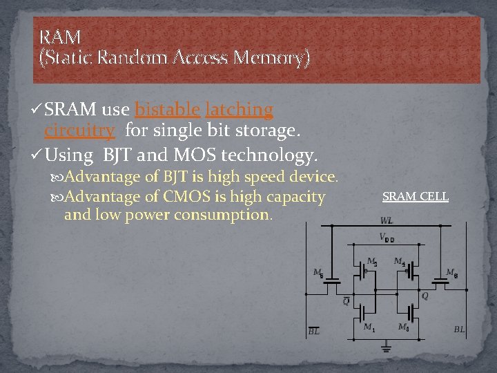
RAM (Static Random Access Memory) ü SRAM use bistable latching circuitry for single bit storage. ü Using BJT and MOS technology. Advantage of BJT is high speed device. Advantage of CMOS is high capacity and low power consumption. SRAM CELL

RAM (Static Random Access Memory) STATIC RAM (SRAM) Can store data as long as power is applied to the chip. SRAM memory cells are essentially flip-flops that will stay in a given state (store a bit) indefinitely provide that power to the circuit is not interrupted. Main applications of SRAM are used in various electronic applications including toys, automobiles, digital devices and computers.

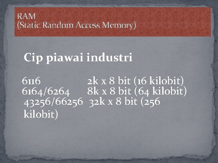
RAM (Static Random Access Memory) Cip piawai industri 6116 2 k x 8 bit (16 kilobit) 6164/6264 8 k x 8 bit (64 kilobit) 43256/66256 32 k x 8 bit (256 kilobit)

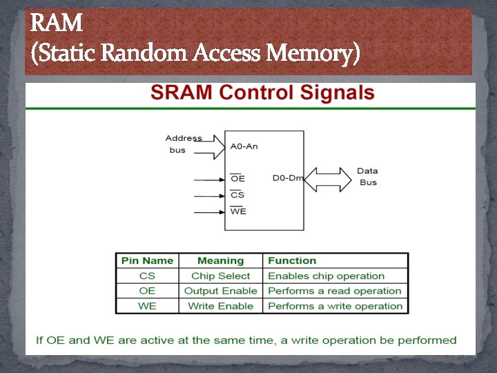
RAM (Static Random Access Memory)

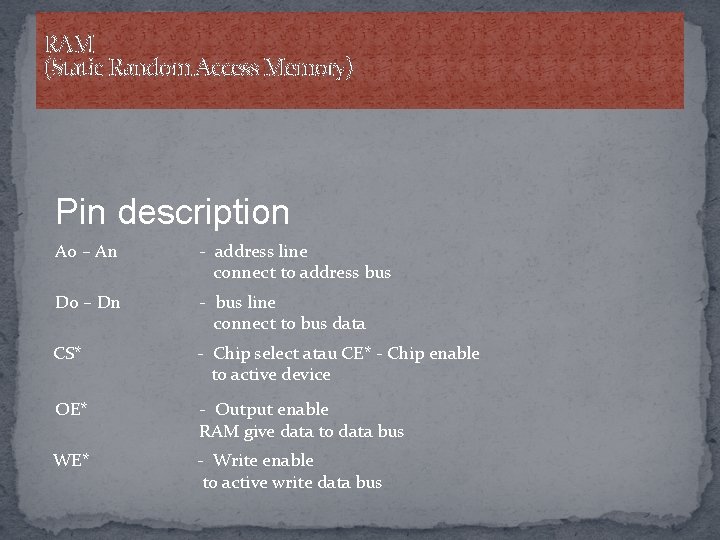
RAM (Static Random Access Memory) Pin description A 0 – An - address line connect to address bus D 0 – Dn - bus line connect to bus data CS* - Chip select atau CE* - Chip enable to active device OE* - Output enable RAM give data to data bus WE* - Write enable to active write data bus

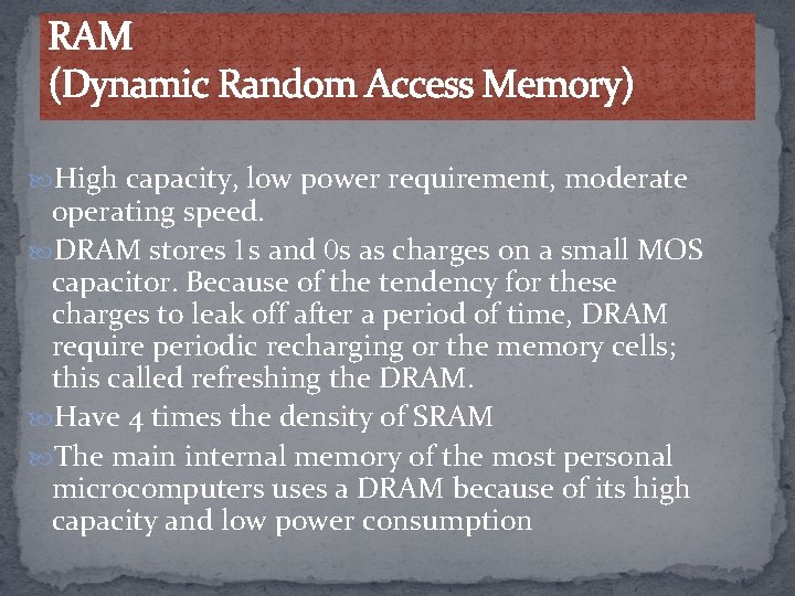
RAM (Dynamic Random Access Memory) High capacity, low power requirement, moderate operating speed. DRAM stores 1 s and 0 s as charges on a small MOS capacitor. Because of the tendency for these charges to leak off after a period of time, DRAM require periodic recharging or the memory cells; this called refreshing the DRAM. Have 4 times the density of SRAM The main internal memory of the most personal microcomputers uses a DRAM because of its high capacity and low power consumption

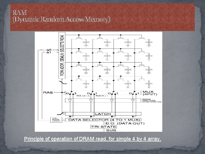
RAM (Dynamic Random Access Memory) DRAM - Operation principle DRAM is usually arranged in a square array of one capacitor and transistor per cell. The illustrations to the right show a simple example with only 4 by 4 cells (modern DRAM can be thousands of cells in length/width). The long lines connecting each row are known as word lines. Each column is actually composed of two bit lines, each one connected to every other storage cell in the column.

RAM (Dynamic Random Access Memory) Principle of operation of DRAM read, for simple 4 by 4 array.

RAM (Dynamic Random Access Memory) Jenis-jenis DRAM 1. FPM DRAM – Fast page mode DRAM membolehkan data dicapai dengan cepat pada ‘page’ yang sama (beberapa alamat dalam julat tertentu) 2. EDO DRAM – Extended Data Output DRAM membaiki ciri FPM dari segi cara membaca dan menulis data. 3. SDRAM – Synchronous DRAM mempunyai ciri membaca data dengan lebih laju.

Different between ROM and RAM � ROM : Read-Only Memory � Non-volatile (data retained even without power) � Exists on all computers � Functions on general-purpose computer: power-on self test, basic input/output system (BIOS), monitor program, etc. � Functions on embedded systems: power-on self test, monitor program, application program. � RAM : Random Access Memory � Volatile (data disappears without power) � Functions on general purpose computer: main memory for running operating system and application program � Functions on embedded systems: scratch-pad memory � May not be required on very simple embedded systems

Introduction to address decoding Full address decoding Partial address decoding Implementing address decoders Examples

Memory Map and Address Decoding Different portions of memory are used for different purposes: RAM, ROM, I/O devices Even if all the memory was of one type, we still have to implement it using different and unique addressing. This means that for a given valid address, one and only one memory-mapped component must be accessed. Address decoding is the process of generating chip select (CS*) signals from the address bus for each device in the system

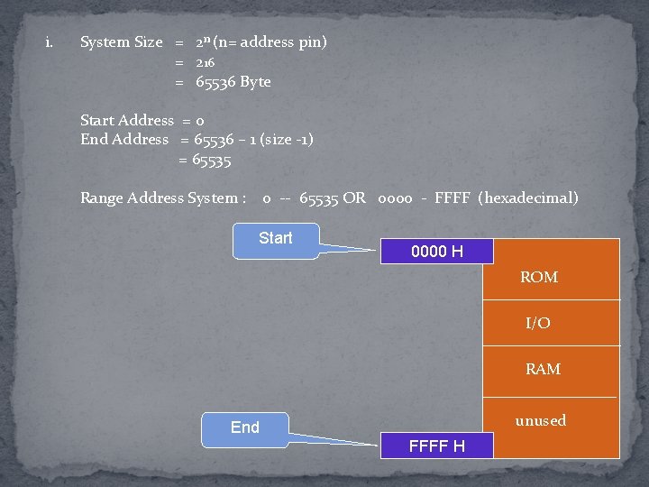
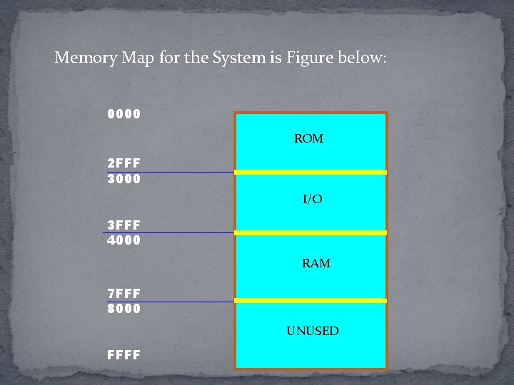
Contoh : Let’s assume a very simple system like that: > CPU 8 bit data bus line > 16 bit address bus line > 12 Kbyte ROM > 4 Kbyte for I/O ports > 16 Kbyte RAM Make a sample memory map for that system.

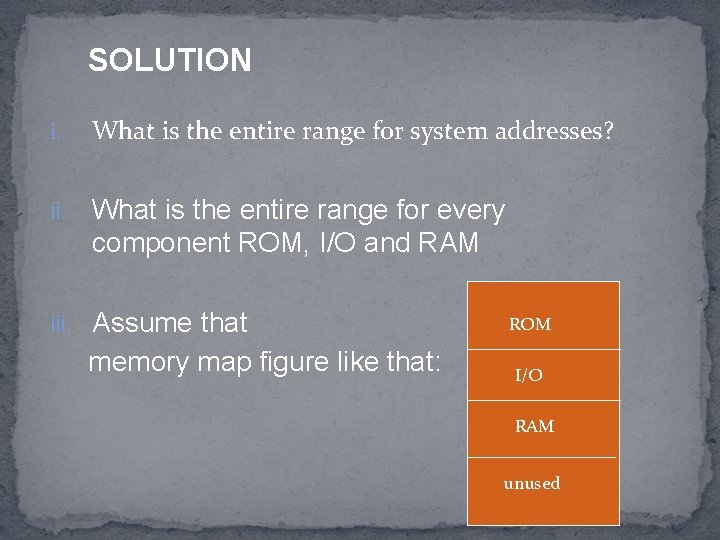
SOLUTION i. What is the entire range for system addresses? ii. What is the entire range for every component ROM, I/O and RAM iii. Assume that memory map figure like that: ROM I/O RAM unused

i. System Size = 2 n (n= address pin) = 216 = 65536 Byte Start Address = 0 End Address = 65536 – 1 (size -1) = 65535 Range Address System : 0 -- 65535 OR 0000 - FFFF (hexadecimal) Start 0000 H ROM I/O RAM unused End FFFF H

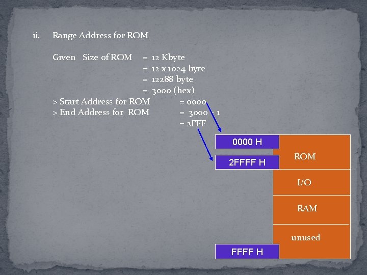
ii. Range Address for ROM Given Size of ROM = 12 Kbyte = 12 x 1024 byte = 12288 byte = 3000 (hex) > Start Address for ROM = 0000 > End Address for ROM = 3000 – 1 = 2 FFF 0000 H 2 FFFF H ROM I/O RAM unused FFFF H

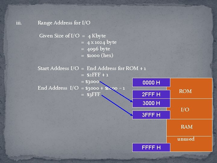
iii. Range Address for I/O Given Size of I/O = = 4 Kbyte 4 x 1024 byte 4096 byte $1000 (hex) Start Address I/O = End Address for ROM + 1 = $2 FFF + 1 = $3000 0000 H End Address I/O = $3000 + $1000 – 1 = $3 FFF 2 FFF H ROM 3000 H 3 FFF H I/O RAM unused FFFF H

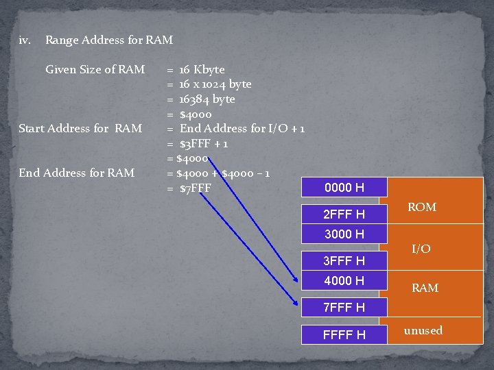
iv. Range Address for RAM Given Size of RAM Start Address for RAM End Address for RAM = 16 Kbyte = 16 x 1024 byte = 16384 byte = $4000 = End Address for I/O + 1 = $3 FFF + 1 = $4000 + $4000 – 1 = $7 FFF 0000 H 2 FFF H ROM 3000 H 3 FFF H 4000 H I/O RAM 7 FFF H FFFF H unused

Memory Map for the System is Figure below: 0000 ROM 2 FFF 3000 I/O 3 FFF 4000 RAM 7 FFF 8000 UNUSED FFFF

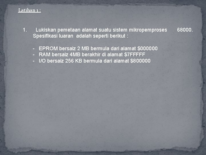
Latihan 1 : 1. Lukiskan pemetaan alamat suatu sistem mikropemproses Spesifikasi luaran adalah seperti berikut : - EPROM bersaiz 2 MB bermula dari alamat $000000 - RAM bersaiz 4 MB berakhir di alamat $7 FFFFF - I/O bersaiz 256 KB bermula dari alamat $800000 68000.

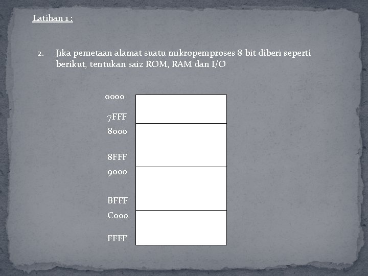
Latihan 1 : 2. Jika pemetaan alamat suatu mikropemproses 8 bit diberi seperti berikut, tentukan saiz ROM, RAM dan I/O 0000 7 FFF RAM 8000 8 FFF I/O 9000 UNUSED BFFF C 000 FFFF ROM

Penyahkod Alamat Dalam suatu sistem komputer, terdapat beberapa peranti yang berada di bawah kawalan pemproses. Pada satu masa, pemproses hanya boleh bertukar data atau berinteraksi hanya dengan satu peranti sahaja. Pemilihan peranti ditentukan oleh kedudukannya dalam peta ingatan. Jadi penyahkod alamat (address decoder) diperlukan bagi memilih peranti yang hendak diaktifkan.

Untuk merekabentuk penyahkod alamat, terdapat beberapa langkah iaitu : i. Tentukan julat alamat untuk peranti (rujuk peta ingatan) ii. Bilangan cip yang diperlukan iii. Bilangan talian alamat pada cip (talian alamat rendah dari pemproses ke cip) iv. Baki talian alamat masuk ke penyahkod alamat v. Lukis litar penyambungan antara komponen berkaitan.

Contoh : Lukiskan sambungan penyahkod alamat bagi suatu sistem komputer yang mempunyai kapasiti ingatan 256 x 4 bit. Diberi satu cip ingatan RAM 64 x 4 bit dan peta ingatan seperti berikut : Peta Ingatan 00 RAM FF terdapat 256 ruang alamat

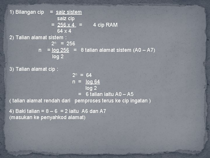
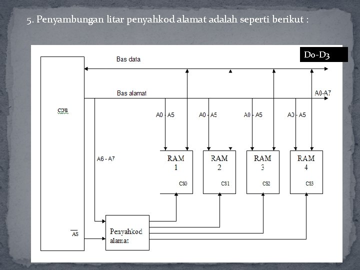
1) Bilangan cip = saiz sistem saiz cip = 256 x 4 = 4 cip RAM 64 x 4 2) Talian alamat sistem : 2 n = 256 n = log 256 = 8 talian alamat sistem (A 0 – A 7) log 2 3) Talian alamat cip : 2 n = 64 n = log 64 log 2 = 6 talian iaitu A 0 – A 5 ( talian alamat rendah dari pemproses terus ke cip ingatan ) 4) Baki talian = 8 – 6 = 2 iaitu A 6 dan A 7 (masukan ke penyahkod alamat)

5. Penyambungan litar penyahkod alamat adalah seperti berikut : D 0 -D 3

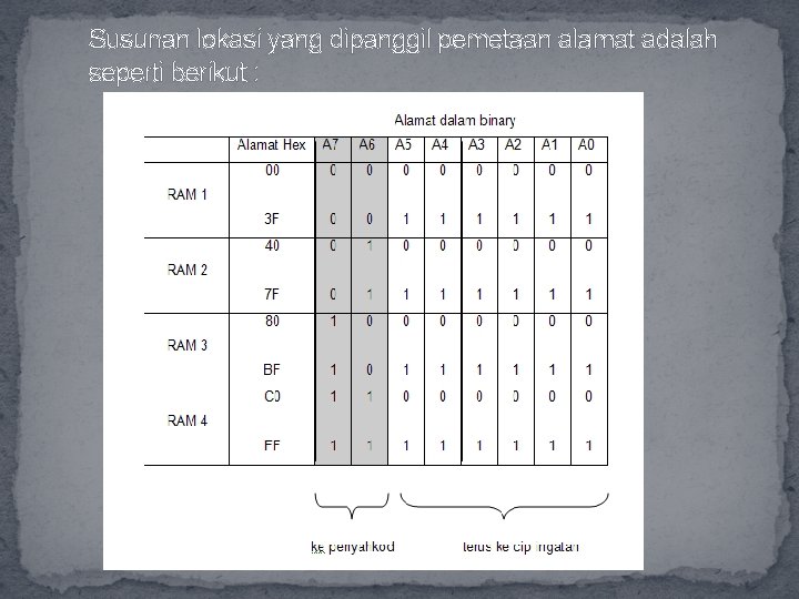
Penerangan Talian teratas A 6 dan A 7 disambungkan ke penyahkod alamat. Litar penyahkod berfungsi memilih satu daripada 4 cip ingatan tersebut. Penyahkod yang digunakan adalah ‘ 2 - line to 4 - line’ Setiap cip mempunyai CS input masing-masing. Jika A 6 dan A 7 berlogik ‘ 0’, maka pin CS 0 akan aktif iaitu logic ‘ 0’. Ini bermakna RAM 1 akan dipilih. Lokasi ingatan yang digunakan antara setiap cip ingatan ditentukan oleh talian A 0 hingga A 5.

Susunan lokasi yang dipanggil pemetaan alamat adalah seperti berikut :

Kaedah untuk menentukan talian yang masuk ke cip dan baki talian yang masuk ke penyahkod Disamping itu terdapat satu lagi kaedah untuk menentukan talian yang masuk ke cip dan baki talian yang masuk ke penyahkod alamat iaitu dengan merujuk kepada peta ingatan. Alamat mula ROM 1 = $ 00 0 0 0 0 Alamat akhir ROM 1 = $ 3 F 0 0 1 1 1 Mula dari kanan : Bit yang bernilai 0 di alamat mula dan 1 di alamat akhir pergi terus ke ingatan. Di sini A 0 hingga A 5 pergi terus ke ingatan. Baki talian iaitu A 6 – A 7 pergi ke penyahkod. Perhatikan nilai-nilai A 6 - A 7 dimana setiap cip mempunyai nilai yang berbeza dan nilai ini yang menentukan cip yang akan diaktifkan.

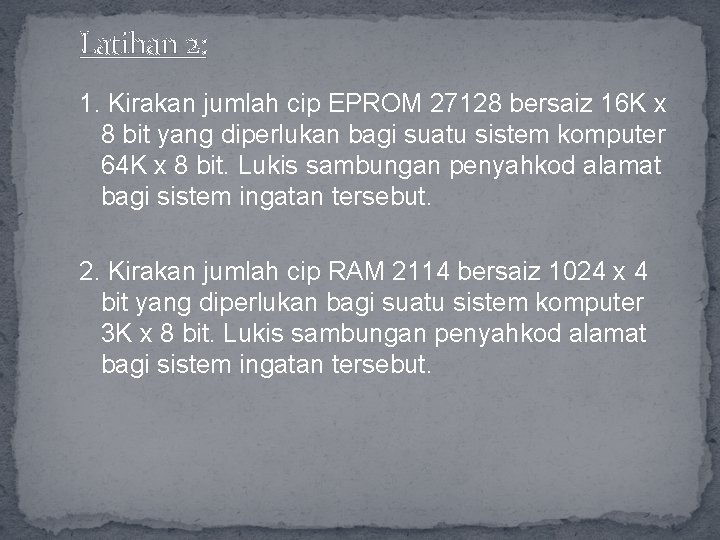
Latihan 2: 1. Kirakan jumlah cip EPROM 27128 bersaiz 16 K x 8 bit yang diperlukan bagi suatu sistem komputer 64 K x 8 bit. Lukis sambungan penyahkod alamat bagi sistem ingatan tersebut. 2. Kirakan jumlah cip RAM 2114 bersaiz 1024 x 4 bit yang diperlukan bagi suatu sistem komputer 3 K x 8 bit. Lukis sambungan penyahkod alamat bagi sistem ingatan tersebut.