Introduction to FPGA Devices ECE 645 Computer Arithmetic



- Slides: 52

Introduction to FPGA Devices ECE 645 – Computer Arithmetic George Mason University

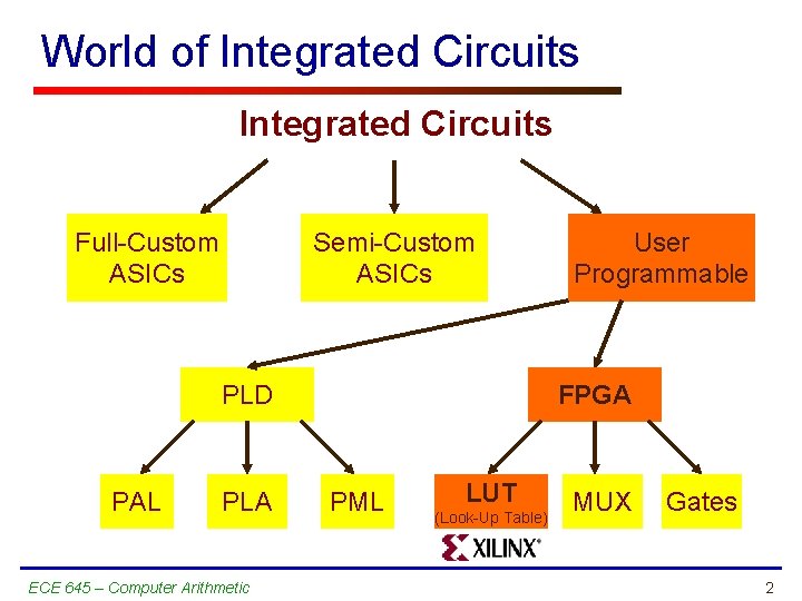
World of Integrated Circuits Full-Custom ASICs Semi-Custom ASICs PLD PAL PLA ECE 645 – Computer Arithmetic User Programmable FPGA PML LUT (Look-Up Table) MUX Gates 2

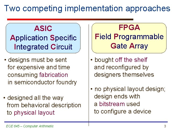
Two competing implementation approaches ASIC Application Specific Integrated Circuit • designs must be sent for expensive and time consuming fabrication in semiconductor foundry • designed all the way from behavioral description to physical layout ECE 645 – Computer Arithmetic FPGA Field Programmable Gate Array • bought off the shelf and reconfigured by designers themselves • no physical layout design; design ends with a bitstream used to configure a device 3

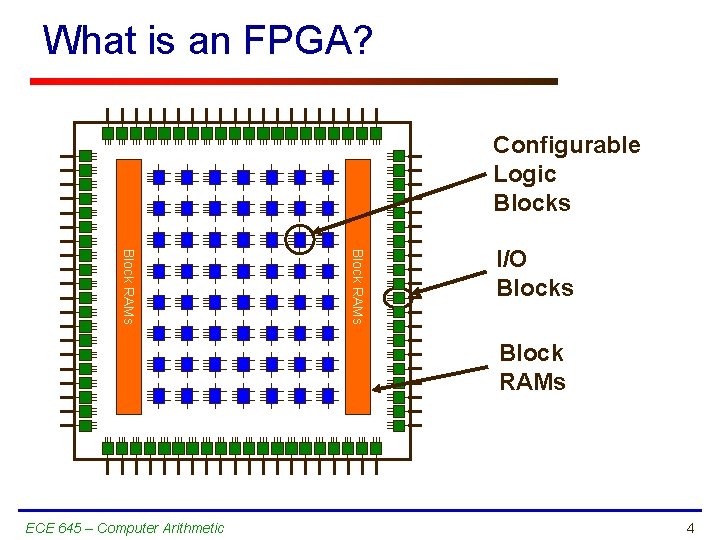
What is an FPGA? Configurable Logic Blocks Block RAMs I/O Blocks Block RAMs ECE 645 – Computer Arithmetic 4

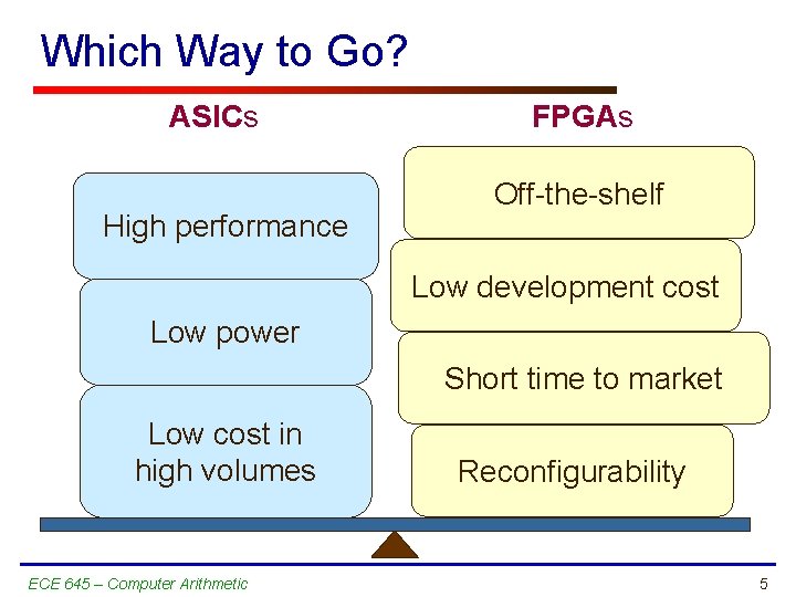
Which Way to Go? ASICs High performance FPGAs Off-the-shelf Low development cost Low power Short time to market Low cost in high volumes ECE 645 – Computer Arithmetic Reconfigurability 5

Other FPGA Advantages • Manufacturing cycle for ASIC is very costly, lengthy and engages lots of manpower • Mistakes not detected at design time have large impact on development time and cost • FPGAs are perfect for rapid prototyping of digital circuits • Easy upgrades like in case of software • Unique applications • reconfigurable computing ECE 645 – Computer Arithmetic 6

Major FPGA Vendors SRAM-based FPGAs • Xilinx, Inc. Share over 60% of the market • Altera Corp. • Atmel • Lattice Semiconductor Flash & antifuse FPGAs • Actel Corp. • Quick Logic Corp. ECE 645 – Computer Arithmetic 7

Xilinx u Primary products: FPGAs and the associated CAD software Programmable Logic Devices u u ISE Alliance and Foundation Series Design Software Main headquarters in San Jose, CA Fabless* Semiconductor and Software Company u u u UMC (Taiwan) {*Xilinx acquired an equity stake in UMC in 1996} Seiko Epson (Japan) TSMC (Taiwan) ECE 645 – Computer Arithmetic 8

Xilinx FPGA Families • Old families • XC 3000, XC 4000, XC 5200 • Old 0. 5µm, 0. 35µm and 0. 25µm technology. Not recommended for modern designs. • High-performance families • • Virtex (0. 22µm) Virtex-E, Virtex-EM (0. 18µm) Virtex-II, Virtex-II PRO (0. 13µm) Virtex-4 (0. 09µm) • Low Cost Family • • Spartan/XL – derived from XC 4000 Spartan-II – derived from Virtex Spartan-IIE – derived from Virtex-E Spartan-3 ECE 645 – Computer Arithmetic 9

ECE 645 – Computer Arithmetic 10

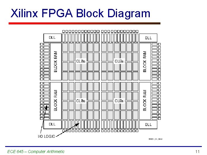
Xilinx FPGA Block Diagram ECE 645 – Computer Arithmetic 11

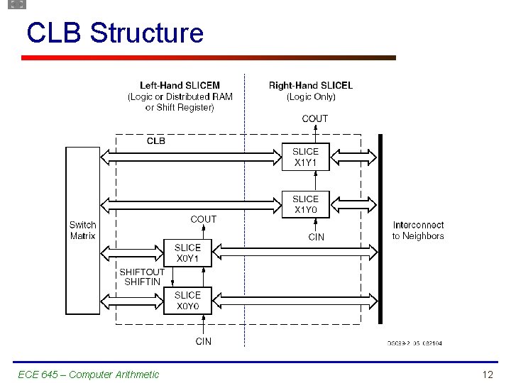
CLB Structure ECE 645 – Computer Arithmetic 12

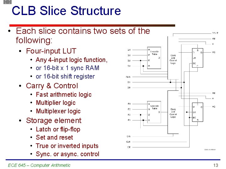
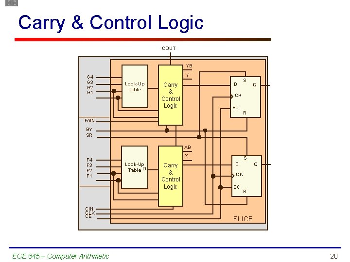
CLB Slice Structure • Each slice contains two sets of the following: • Four-input LUT • Any 4 -input logic function, • or 16 -bit x 1 sync RAM • or 16 -bit shift register • Carry & Control • Fast arithmetic logic • Multiplier logic • Multiplexer logic • Storage element • • Latch or flip-flop Set and reset True or inverted inputs Sync. or async. control ECE 645 – Computer Arithmetic 13

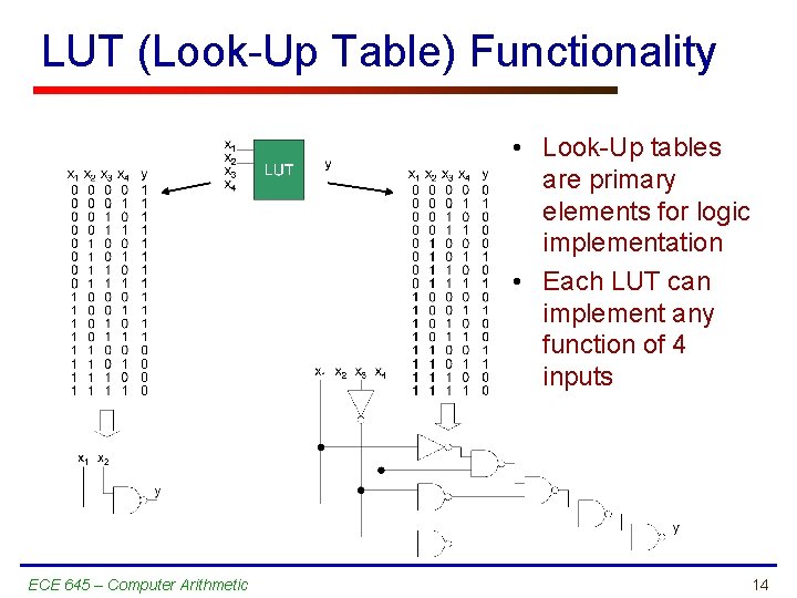
LUT (Look-Up Table) Functionality • Look-Up tables are primary elements for logic implementation • Each LUT can implement any function of 4 inputs ECE 645 – Computer Arithmetic 14

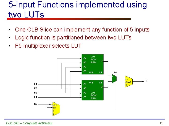
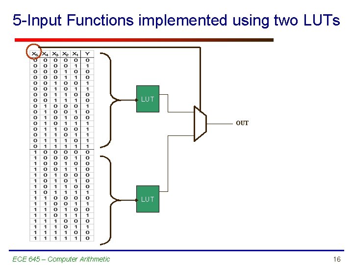
5 -Input Functions implemented using two LUTs • One CLB Slice can implement any function of 5 inputs • Logic function is partitioned between two LUTs • F 5 multiplexer selects LUT ECE 645 – Computer Arithmetic 15

5 -Input Functions implemented using two LUTs LUT OUT LUT ECE 645 – Computer Arithmetic 16

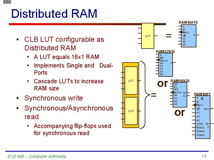
Distributed RAM 16 X 1 S • A LUT equals 16 x 1 RAM • Implements Single and Dual. Ports • Cascade LUTs to increase RAM size • Synchronous write • Synchronous/Asynchronous read • Accompanying flip-flops used for synchronous read ECE 645 – Computer Arithmetic = LUT • CLB LUT configurable as Distributed RAM D W EWCL K A 0 A 1 A 2 A 3 O RAM 32 X 1 S D WE WCLK A 0 A 1 A 2 A 3 A 4 LUT = LUT or O RAM 16 X 2 S D 0 D 1 WE WCLK O 0 A 0 O 1 A 2 A 3 or RAM 16 X 1 D D W EWCL K A 0 SPO A 1 A 2 A 3 DPRA DP 0 DPRA 1 O DPRA 2 DPRA 3 17

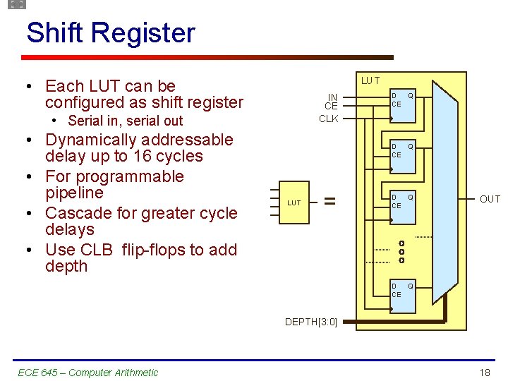
Shift Register LUT • Each LUT can be configured as shift register IN CE CLK • Serial in, serial out • Dynamically addressable delay up to 16 cycles • For programmable pipeline • Cascade for greater cycle delays • Use CLB flip-flops to add depth D Q CE LUT = D Q CE OUT D Q CE DEPTH[3: 0] ECE 645 – Computer Arithmetic 18

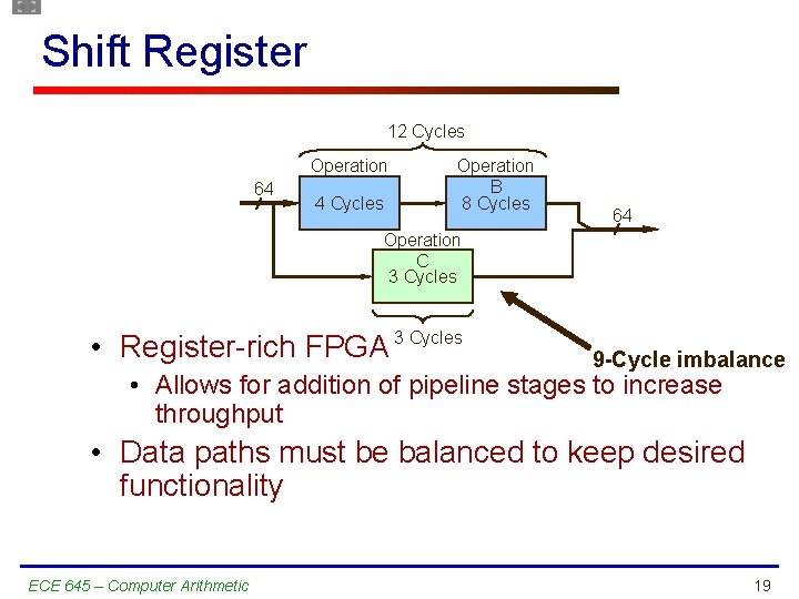
Shift Register 12 Cycles 64 Operation A 4 Cycles Operation B 8 Cycles 64 Operation C 3 Cycles • Register-rich FPGA 3 Cycles 9 -Cycle imbalance • Allows for addition of pipeline stages to increase throughput • Data paths must be balanced to keep desired functionality ECE 645 – Computer Arithmetic 19

Carry & Control Logic COUT YB G 4 G 3 G 2 G 1 Y Look-Up O Table D Carry & Control Logic S Q CK EC R F 5 IN BY SR XB F 4 F 3 F 2 F 1 CIN CLK CE ECE 645 – Computer Arithmetic X Look-Up Table O Carry & Control Logic S D Q CK EC R SLICE 20

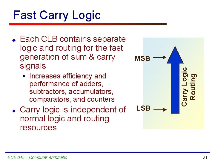
Fast Carry Logic Each CLB contains separate logic and routing for the fast generation of sum & carry signals MSB • Increases efficiency and performance of adders, subtractors, accumulators, comparators, and counters u Carry logic is independent of normal logic and routing resources ECE 645 – Computer Arithmetic LSB Carry Logic Routing u 21

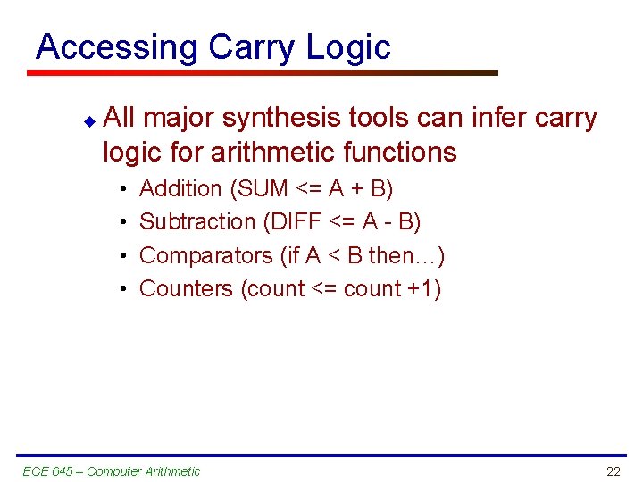
Accessing Carry Logic u All major synthesis tools can infer carry logic for arithmetic functions • • Addition (SUM <= A + B) Subtraction (DIFF <= A - B) Comparators (if A < B then…) Counters (count <= count +1) ECE 645 – Computer Arithmetic 22

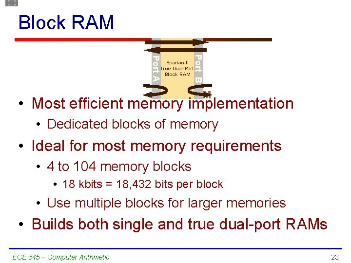
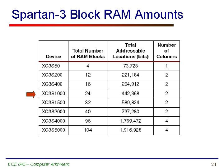
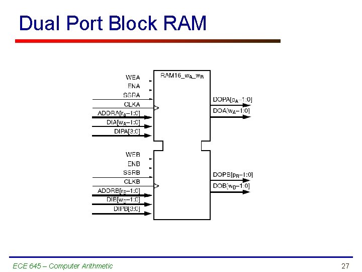
Block RAM Port B Port A Spartan-II True Dual-Port Block RAM • Most efficient memory implementation • Dedicated blocks of memory • Ideal for most memory requirements • 4 to 104 memory blocks • 18 kbits = 18, 432 bits per block • Use multiple blocks for larger memories • Builds both single and true dual-port RAMs ECE 645 – Computer Arithmetic 23

Spartan-3 Block RAM Amounts ECE 645 – Computer Arithmetic 24

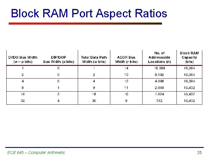
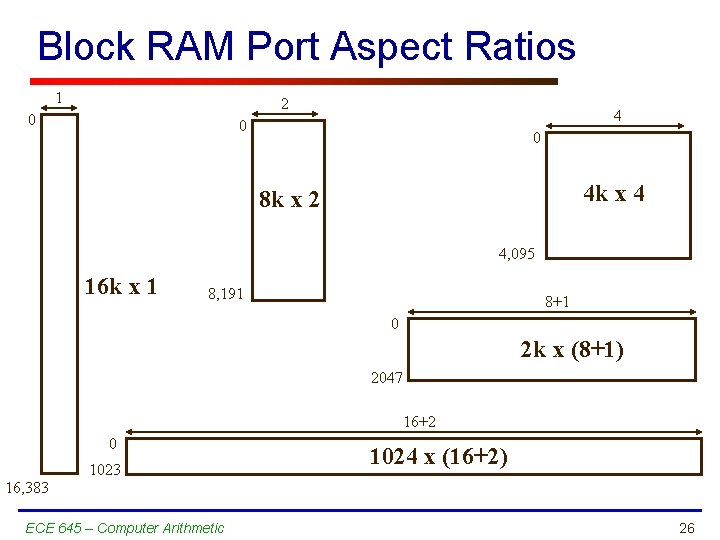
Block RAM Port Aspect Ratios ECE 645 – Computer Arithmetic 25

Block RAM Port Aspect Ratios 1 2 0 4 0 0 4 k x 4 8 k x 2 4, 095 16 k x 1 8, 191 8+1 0 2 k x (8+1) 2047 16+2 0 1023 1024 x (16+2) 16, 383 ECE 645 – Computer Arithmetic 26

Dual Port Block RAM ECE 645 – Computer Arithmetic 27

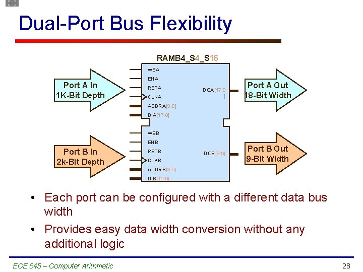
Dual-Port Bus Flexibility RAMB 4_S 16 WEA Port A In 1 K-Bit Depth ENA RSTA CLKA DOA[17: 0 ] Port A Out 18 -Bit Width DOB[8: 0] Port B Out 9 -Bit Width ADDRA[9: 0] DIA[17: 0] WEB ENB Port B In 2 k-Bit Depth RSTB CLKB ADDRB[8: 0] DIB[15: 0] • Each port can be configured with a different data bus width • Provides easy data width conversion without any additional logic ECE 645 – Computer Arithmetic 28

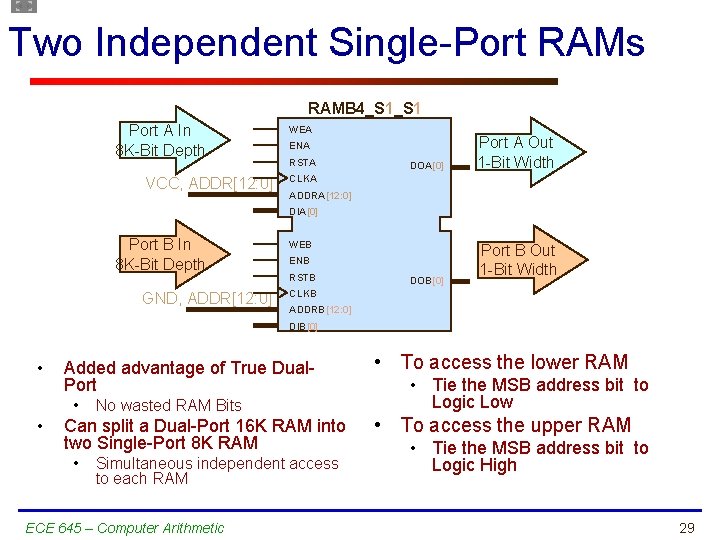
Two Independent Single-Port RAMs RAMB 4_S 1 Port A In 8 K-Bit Depth VCC, ADDR[12: 0] WEA ENA RSTA DOA[0] Port A Out 1 -Bit Width CLKA ADDRA[12: 0] DIA[0] Port B In 8 K-Bit Depth GND, ADDR[12: 0] WEB ENB RSTB DOB[0] Port B Out 1 -Bit Width CLKB ADDRB[12: 0] DIB[0] • Added advantage of True Dual. Port • • No wasted RAM Bits Can split a Dual-Port 16 K RAM into two Single-Port 8 K RAM • Simultaneous independent access to each RAM ECE 645 – Computer Arithmetic • To access the lower RAM • Tie the MSB address bit to Logic Low • To access the upper RAM • Tie the MSB address bit to Logic High 29

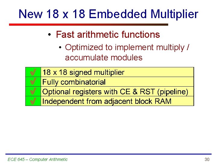
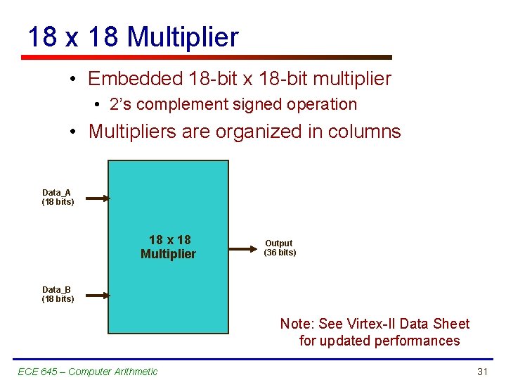
New 18 x 18 Embedded Multiplier • Fast arithmetic functions • Optimized to implement multiply / accumulate modules ECE 645 – Computer Arithmetic 30

18 x 18 Multiplier • Embedded 18 -bit x 18 -bit multiplier • 2’s complement signed operation • Multipliers are organized in columns Data_A (18 bits) 18 x 18 Multiplier Output (36 bits) Data_B (18 bits) Note: See Virtex-II Data Sheet for updated performances ECE 645 – Computer Arithmetic 31

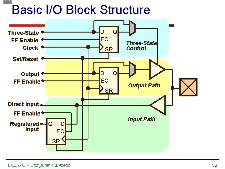
Basic I/O Block Structure D Q EC Three-State FF Enable Clock SR Three-State Control Set/Reset D Q EC Output FF Enable SR Output Path Direct Input FF Enable Registered Input Q D EC Input Path SR ECE 645 – Computer Arithmetic 32

IOB Functionality • IOB provides interface between the package pins and CLBs • Each IOB can work as uni- or bi-directional I/O • Outputs can be forced into High Impedance • Inputs and outputs can be registered • advised for high-performance I/O • Inputs can be delayed ECE 645 – Computer Arithmetic 33

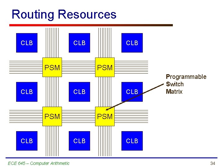
Routing Resources CLB CLB PSM CLB ECE 645 – Computer Arithmetic CLB Programmable Switch Matrix PSM CLB 34

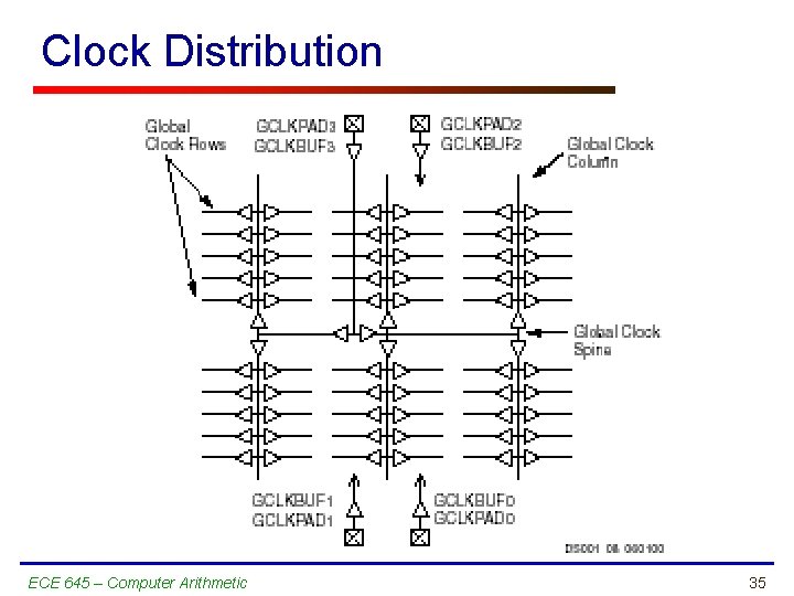
Clock Distribution ECE 645 – Computer Arithmetic 35

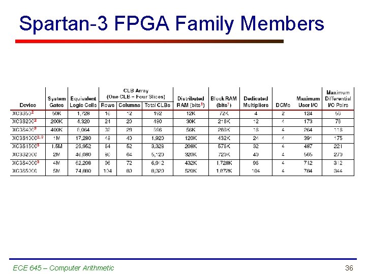
Spartan-3 FPGA Family Members ECE 645 – Computer Arithmetic 36

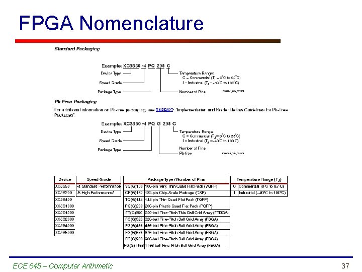
FPGA Nomenclature ECE 645 – Computer Arithmetic 37

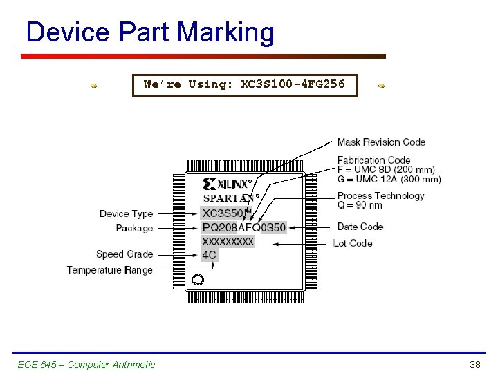
Device Part Marking We’re Using: XC 3 S 100 -4 FG 256 ECE 645 – Computer Arithmetic 38

ECE 645 – Computer Arithmetic 39

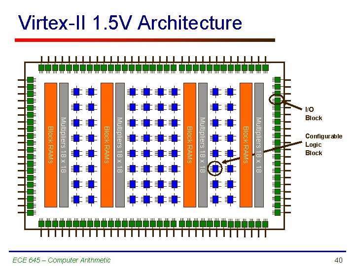
Virtex-II 1. 5 V Architecture Multipliers 18 x 18 Block RAMs Multipliers 18 x 18 Configurable Logic Block RAMs 40 ECE 645 – Computer Arithmetic I/ O Block

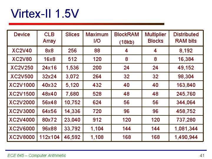
Virtex-II 1. 5 V Device CLB Array Slices Maximum I/O Block. RAM (18 kb) Multiplier Blocks Distributed RAM bits XC 2 V 40 8 x 8 256 88 4 4 8, 192 XC 2 V 80 16 x 8 512 120 8 8 16, 384 XC 2 V 250 24 x 16 1, 536 200 24 24 49, 152 XC 2 V 500 32 x 24 3, 072 264 32 32 98, 304 XC 2 V 1000 40 x 32 5, 120 432 40 40 163, 840 XC 2 V 1500 48 x 40 7, 680 528 48 48 245, 760 XC 2 V 2000 56 x 48 10, 752 624 56 56 344, 064 XC 2 V 3000 64 x 56 14, 336 720 96 96 458, 752 XC 2 V 4000 80 x 72 23, 040 912 120 737, 280 XC 2 V 6000 96 x 88 33, 792 1, 104 144 1, 081, 344 XC 2 V 8000 112 x 104 46, 592 1, 108 168 1, 490, 944 ECE 645 – Computer Arithmetic 41

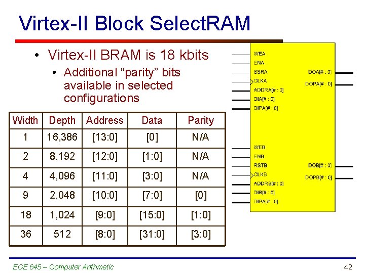
Virtex-II Block Select. RAM • Virtex-II BRAM is 18 kbits • Additional “parity” bits available in selected configurations Width Depth Address Data Parity 1 16, 386 [13: 0] [0] N/A 2 8, 192 [12: 0] [1: 0] N/A 4 4, 096 [11: 0] [3: 0] N/A 9 2, 048 [10: 0] [7: 0] [0] 18 1, 024 [9: 0] [15: 0] [1: 0] 36 512 [8: 0] [31: 0] [3: 0] ECE 645 – Computer Arithmetic 42

Using Library Components in VHDL Code ECE 645 – Computer Arithmetic George Mason University

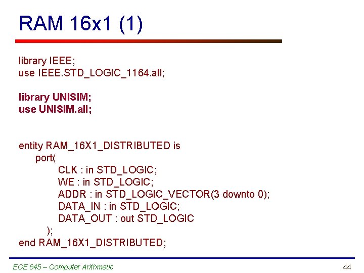
RAM 16 x 1 (1) library IEEE; use IEEE. STD_LOGIC_1164. all; library UNISIM; use UNISIM. all; entity RAM_16 X 1_DISTRIBUTED is port( CLK : in STD_LOGIC; WE : in STD_LOGIC; ADDR : in STD_LOGIC_VECTOR(3 downto 0); DATA_IN : in STD_LOGIC; DATA_OUT : out STD_LOGIC ); end RAM_16 X 1_DISTRIBUTED; ECE 645 – Computer Arithmetic 44

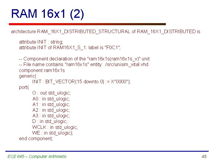
RAM 16 x 1 (2) architecture RAM_16 X 1_DISTRIBUTED_STRUCTURAL of RAM_16 X 1_DISTRIBUTED is attribute INIT : string; attribute INIT of RAM 16 X 1_S_1: label is "F 0 C 1"; -- Component declaration of the "ram 16 x 1 s(ram 16 x 1 s_v)" unit -- File name contains "ram 16 x 1 s" entity: . /src/unisim_vital. vhd component ram 16 x 1 s generic( INIT : BIT_VECTOR(15 downto 0) : = X"0000"); port( O : out std_ulogic; A 0 : in std_ulogic; A 1 : in std_ulogic; A 2 : in std_ulogic; A 3 : in std_ulogic; D : in std_ulogic; WCLK : in std_ulogic; WE : in std_ulogic); end component; ECE 645 – Computer Arithmetic 45

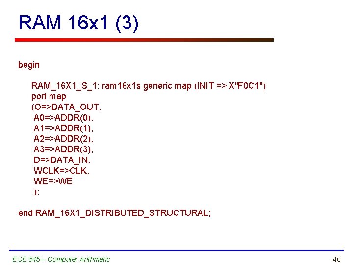
RAM 16 x 1 (3) begin RAM_16 X 1_S_1: ram 16 x 1 s generic map (INIT => X"F 0 C 1") port map (O=>DATA_OUT, A 0=>ADDR(0), A 1=>ADDR(1), A 2=>ADDR(2), A 3=>ADDR(3), D=>DATA_IN, WCLK=>CLK, WE=>WE ); end RAM_16 X 1_DISTRIBUTED_STRUCTURAL; ECE 645 – Computer Arithmetic 46

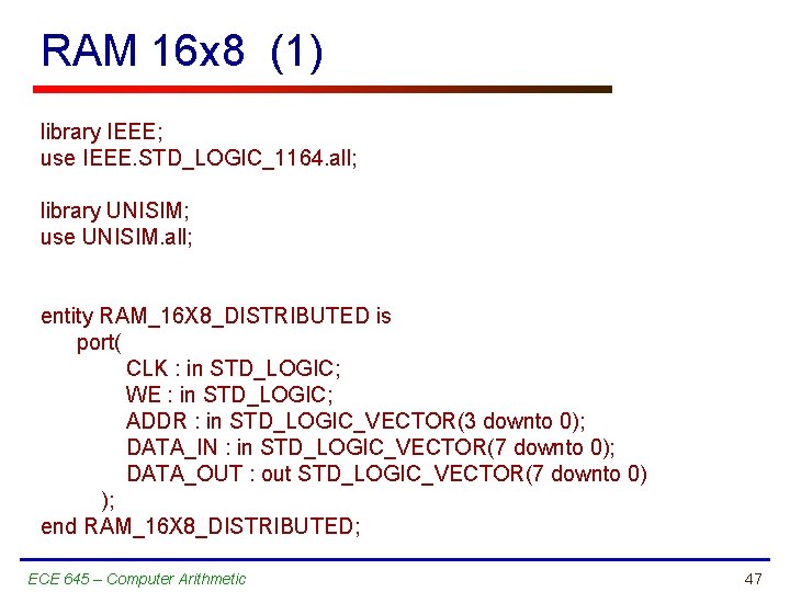
RAM 16 x 8 (1) library IEEE; use IEEE. STD_LOGIC_1164. all; library UNISIM; use UNISIM. all; entity RAM_16 X 8_DISTRIBUTED is port( CLK : in STD_LOGIC; WE : in STD_LOGIC; ADDR : in STD_LOGIC_VECTOR(3 downto 0); DATA_IN : in STD_LOGIC_VECTOR(7 downto 0); DATA_OUT : out STD_LOGIC_VECTOR(7 downto 0) ); end RAM_16 X 8_DISTRIBUTED; ECE 645 – Computer Arithmetic 47

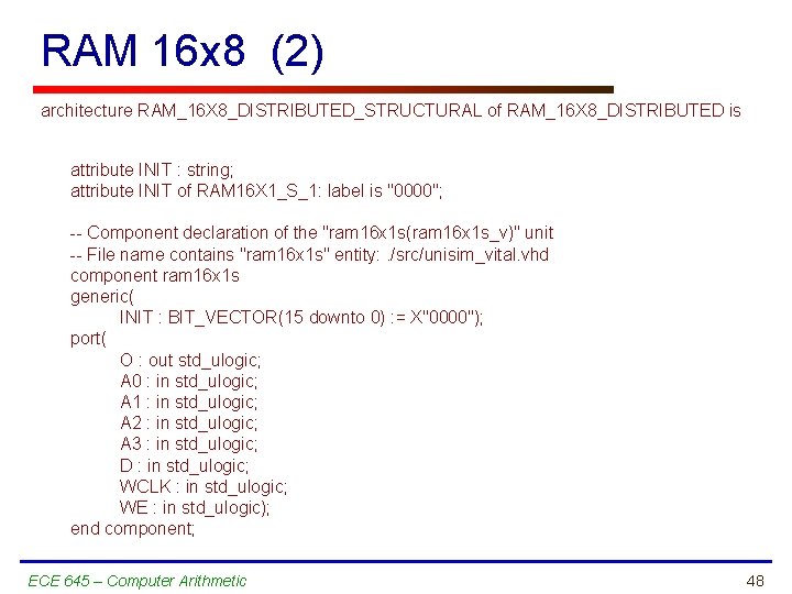
RAM 16 x 8 (2) architecture RAM_16 X 8_DISTRIBUTED_STRUCTURAL of RAM_16 X 8_DISTRIBUTED is attribute INIT : string; attribute INIT of RAM 16 X 1_S_1: label is "0000"; -- Component declaration of the "ram 16 x 1 s(ram 16 x 1 s_v)" unit -- File name contains "ram 16 x 1 s" entity: . /src/unisim_vital. vhd component ram 16 x 1 s generic( INIT : BIT_VECTOR(15 downto 0) : = X"0000"); port( O : out std_ulogic; A 0 : in std_ulogic; A 1 : in std_ulogic; A 2 : in std_ulogic; A 3 : in std_ulogic; D : in std_ulogic; WCLK : in std_ulogic; WE : in std_ulogic); end component; ECE 645 – Computer Arithmetic 48

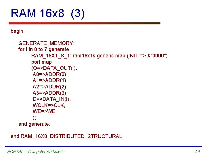
RAM 16 x 8 (3) begin GENERATE_MEMORY: for I in 0 to 7 generate RAM_16 X 1_S_1: ram 16 x 1 s generic map (INIT => X"0000") port map (O=>DATA_OUT(I), A 0=>ADDR(0), A 1=>ADDR(1), A 2=>ADDR(2), A 3=>ADDR(3), D=>DATA_IN(I), WCLK=>CLK, WE=>WE ); end generate; end RAM_16 X 8_DISTRIBUTED_STRUCTURAL; ECE 645 – Computer Arithmetic 49

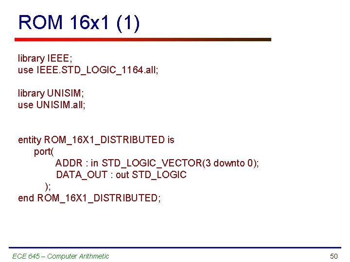
ROM 16 x 1 (1) library IEEE; use IEEE. STD_LOGIC_1164. all; library UNISIM; use UNISIM. all; entity ROM_16 X 1_DISTRIBUTED is port( ADDR : in STD_LOGIC_VECTOR(3 downto 0); DATA_OUT : out STD_LOGIC ); end ROM_16 X 1_DISTRIBUTED; ECE 645 – Computer Arithmetic 50

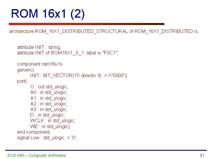
ROM 16 x 1 (2) architecture ROM_16 X 1_DISTRIBUTED_STRUCTURAL of ROM_16 X 1_DISTRIBUTED is attribute INIT : string; attribute INIT of ROM 16 X 1_S_1: label is "F 0 C 1"; component ram 16 x 1 s generic( INIT : BIT_VECTOR(15 downto 0) : = X"0000"); port( O : out std_ulogic; A 0 : in std_ulogic; A 1 : in std_ulogic; A 2 : in std_ulogic; A 3 : in std_ulogic; D : in std_ulogic; WCLK : in std_ulogic; WE : in std_ulogic); end component; signal Low : std_ulogic : = ‘ 0’; ECE 645 – Computer Arithmetic 51

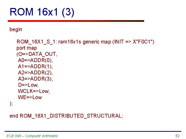
ROM 16 x 1 (3) begin ROM_16 X 1_S_1: ram 16 x 1 s generic map (INIT => X"F 0 C 1") port map (O=>DATA_OUT, A 0=>ADDR(0), A 1=>ADDR(1), A 2=>ADDR(2), A 3=>ADDR(3), D=>Low, WCLK=>Low, WE=>Low ); end ROM_16 X 1_DISTRIBUTED_STRUCTURAL; ECE 645 – Computer Arithmetic 52