ECE 448 Lecture 5 FPGA Devices ECE 448


- Slides: 45

ECE 448 Lecture 5 FPGA Devices ECE 448 – FPGA and ASIC Design with VHDL George Mason University

Required reading • Spartan-6 FPGA Configurable Logic Block: User Guide § § CLB Overview Slice Description 2

Recommended reading Highly recommended for the Wednesday lab section using Nexys 4 boards • 7 Series FPGAs Configurable Logic Block: User Guide § § Overview Functional Details 3

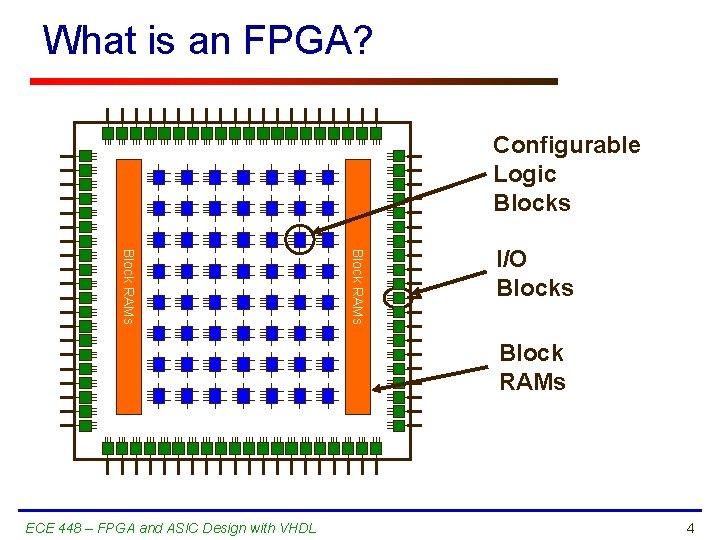
What is an FPGA? Configurable Logic Blocks Block RAMs I/O Blocks Block RAMs ECE 448 – FPGA and ASIC Design with VHDL 4

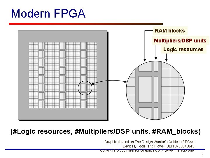
Modern FPGA RAM blocks Multipliers/DSP units Logic resources (#Logic resources, #Multipliers/DSP units, #RAM_blocks) Graphics based on The Design Warrior’s Guide to FPGAs Devices, Tools, and Flows. ISBN 0750676043 Copyright © 2004 Mentor Graphics Corp. (www. mentor. com) 5

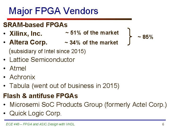
Major FPGA Vendors SRAM-based FPGAs ~ 51% of the market • Xilinx, Inc. ~ 34% of the market • Altera Corp. (subsidiary of Intel since 2015) • Lattice Semiconductor • Atmel • Achronix • Tabula (went out of business in 2015) ~ 85% Flash & antifuse FPGAs • Microsemi So. C Products Group (formerly Actel Corp. ) • Quick Logic Corp. ECE 448 – FPGA and ASIC Design with VHDL 6

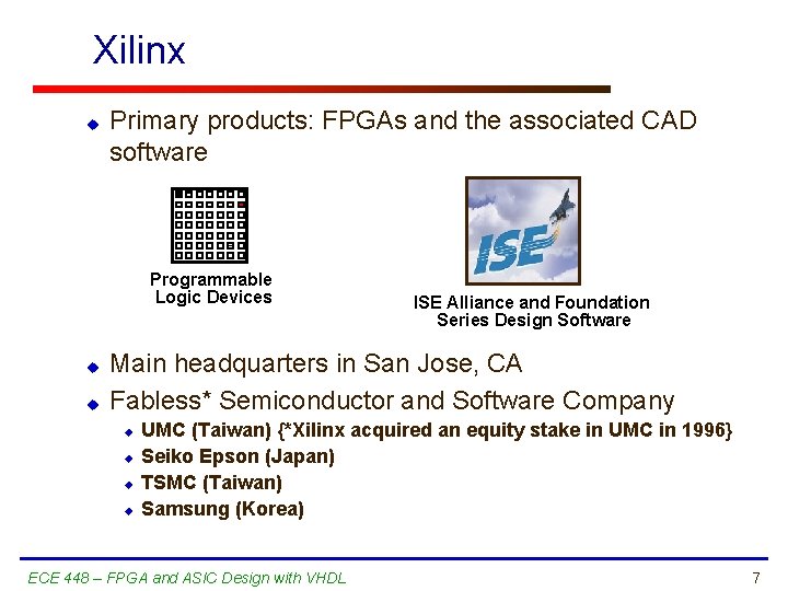
Xilinx u Primary products: FPGAs and the associated CAD software Programmable Logic Devices u u ISE Alliance and Foundation Series Design Software Main headquarters in San Jose, CA Fabless* Semiconductor and Software Company u u UMC (Taiwan) {*Xilinx acquired an equity stake in UMC in 1996} Seiko Epson (Japan) TSMC (Taiwan) Samsung (Korea) ECE 448 – FPGA and ASIC Design with VHDL 7

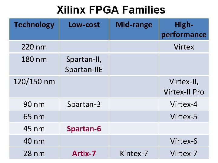
Xilinx FPGA Families Technology 220 nm 180 nm Low-cost Mid-range Spartan-II, Spartan-IIE 120/150 nm 90 nm 65 nm 40 nm 28 nm Highperformance Virtex-II, Virtex-II Pro Virtex-4 Virtex-5 Spartan-3 Spartan-6 Artix-7 Kintex-7 Virtex-6 Virtex-7

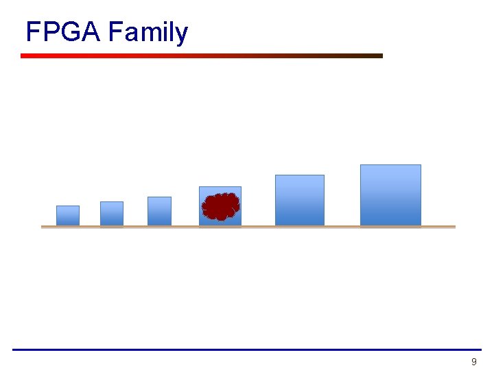
FPGA Family 9

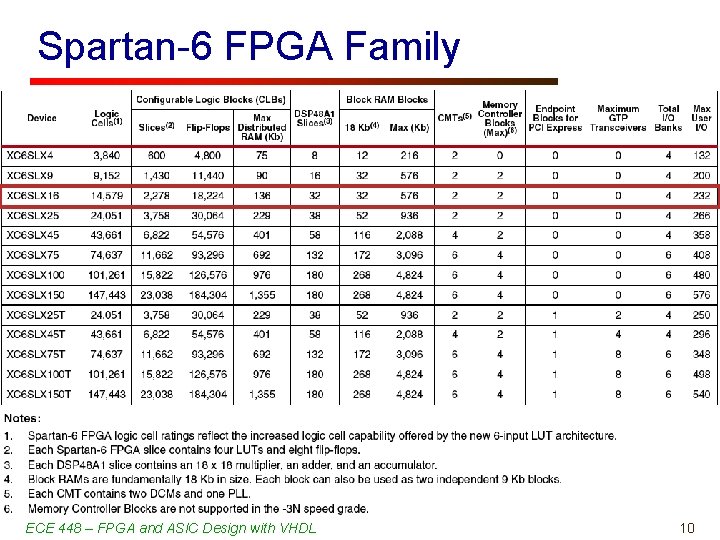
Spartan-6 FPGA Family ECE 448 – FPGA and ASIC Design with VHDL 10

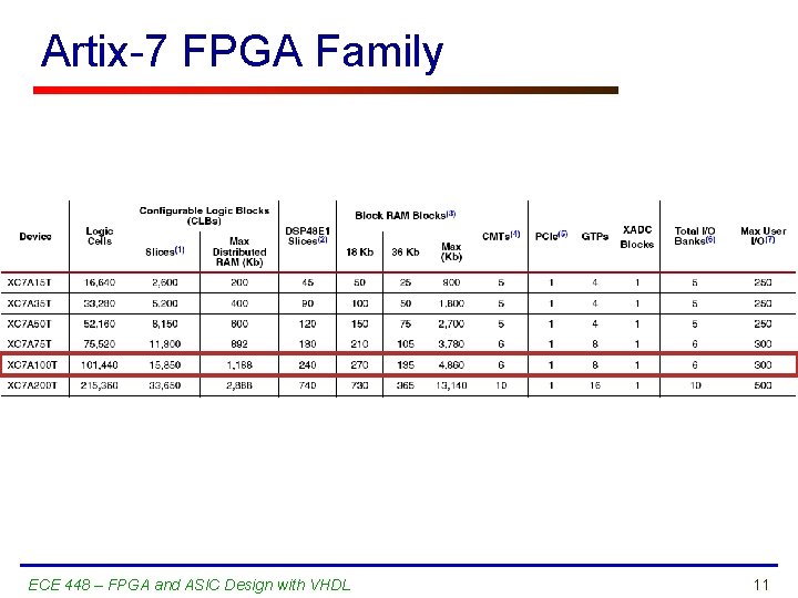
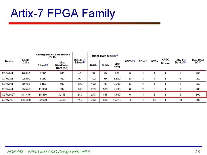
Artix-7 FPGA Family ECE 448 – FPGA and ASIC Design with VHDL 11

CLB Structure ECE 448 – FPGA and ASIC Design with VHDL George Mason University

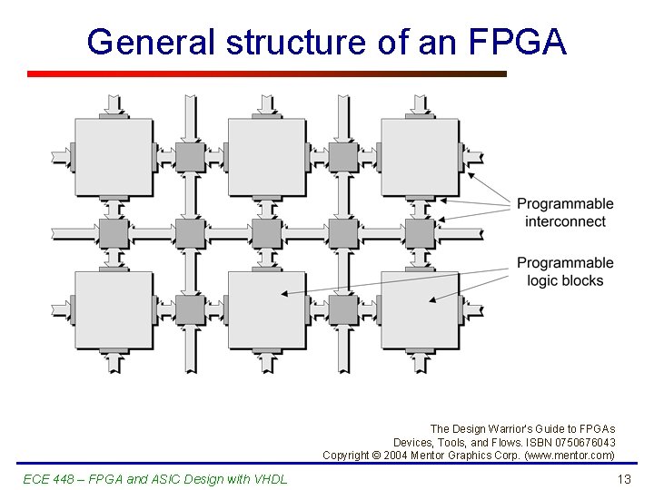
General structure of an FPGA The Design Warrior’s Guide to FPGAs Devices, Tools, and Flows. ISBN 0750676043 Copyright © 2004 Mentor Graphics Corp. (www. mentor. com) ECE 448 – FPGA and ASIC Design with VHDL 13

Xilinx Spartan-6 & Artix-7 CLB ECE 448 – FPGA and ASIC Design with VHDL 14

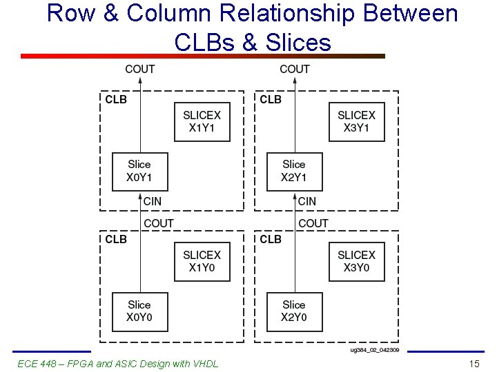
Row & Column Relationship Between CLBs & Slices ECE 448 – FPGA and ASIC Design with VHDL 15

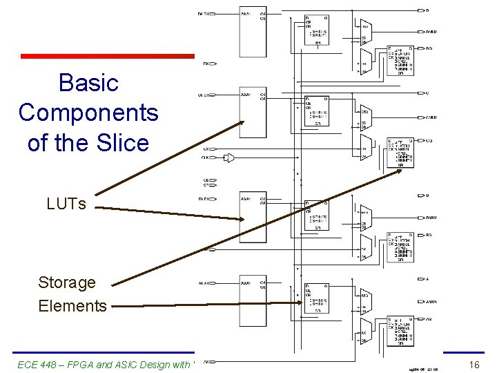
Basic Components of the Slice LUTs Storage Elements ECE 448 – FPGA and ASIC Design with VHDL 16

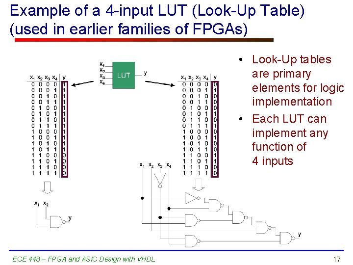
Example of a 4 -input LUT (Look-Up Table) (used in earlier families of FPGAs) • Look-Up tables are primary elements for logic implementation • Each LUT can implement any function of 4 inputs ECE 448 – FPGA and ASIC Design with VHDL 17

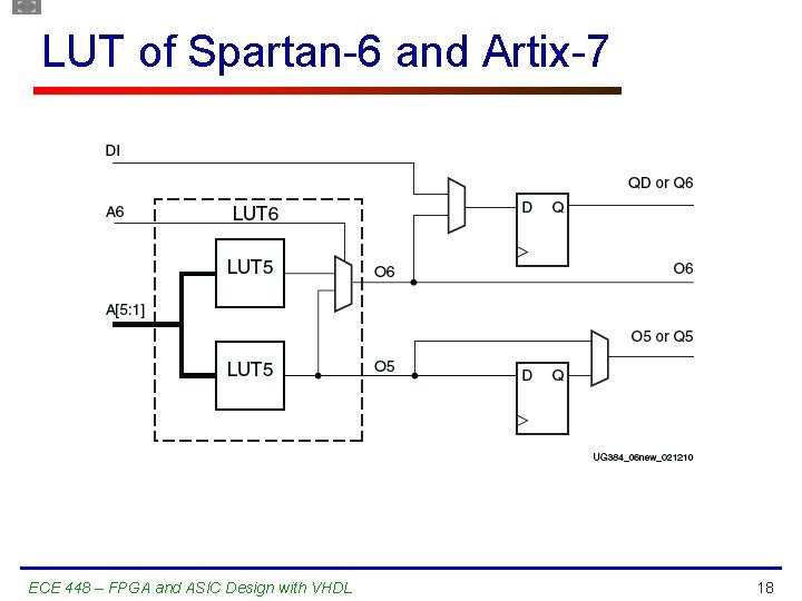
LUT of Spartan-6 and Artix-7 ECE 448 – FPGA and ASIC Design with VHDL 18

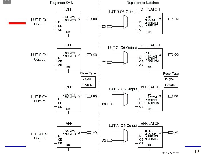
19

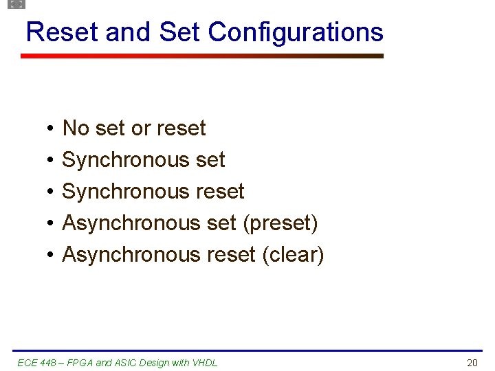
Reset and Set Configurations • • • No set or reset Synchronous reset Asynchronous set (preset) Asynchronous reset (clear) ECE 448 – FPGA and ASIC Design with VHDL 20

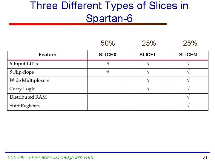
Three Different Types of Slices in Spartan-6 50% ECE 448 – FPGA and ASIC Design with VHDL 25% 21

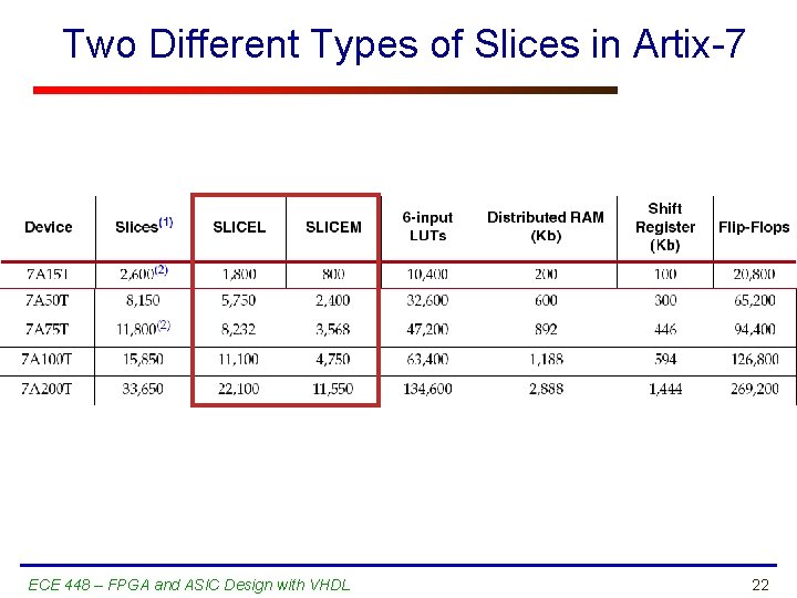
Two Different Types of Slices in Artix-7 ECE 448 – FPGA and ASIC Design with VHDL 22

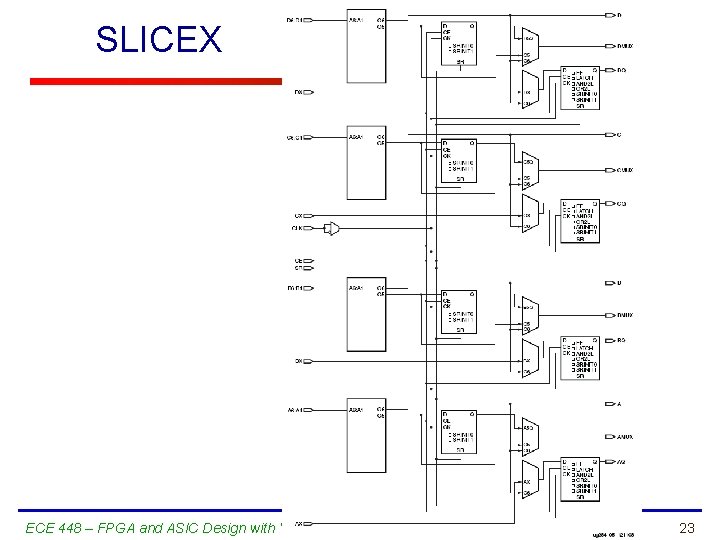
SLICEX ECE 448 – FPGA and ASIC Design with VHDL 23

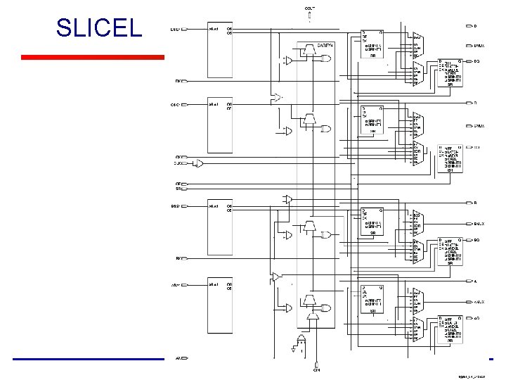
SLICEL 24

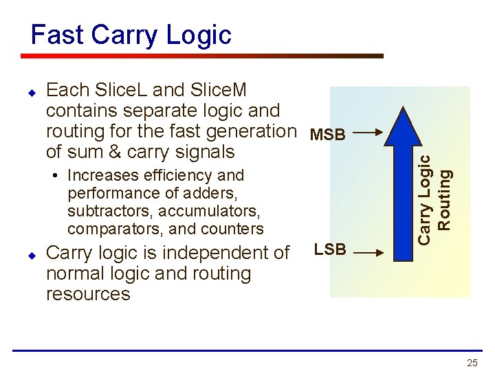
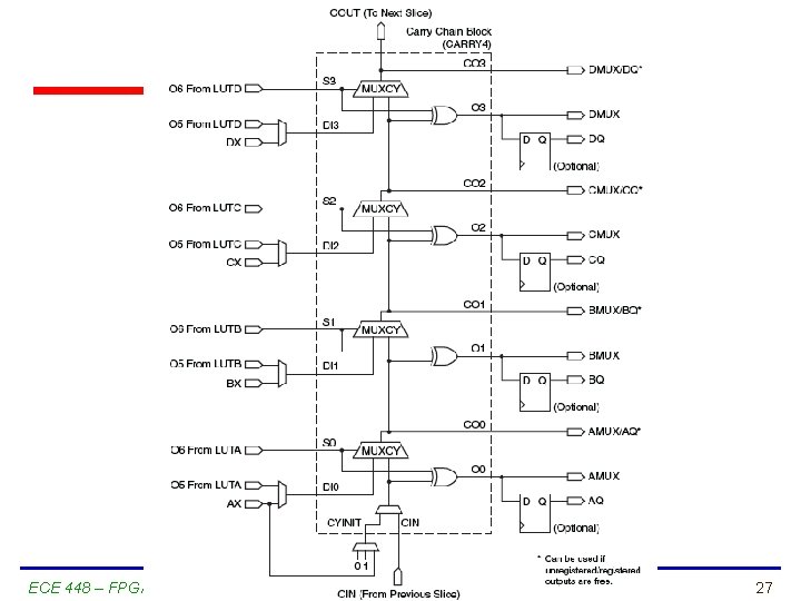
u Each Slice. L and Slice. M contains separate logic and routing for the fast generation MSB of sum & carry signals • Increases efficiency and performance of adders, subtractors, accumulators, comparators, and counters u Carry logic is independent of normal logic and routing resources LSB Carry Logic Routing Fast Carry Logic 25

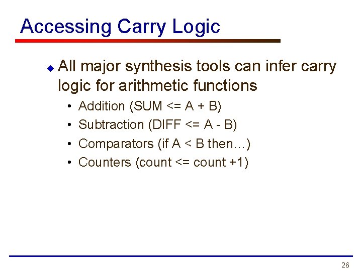
Accessing Carry Logic u All major synthesis tools can infer carry logic for arithmetic functions • • Addition (SUM <= A + B) Subtraction (DIFF <= A - B) Comparators (if A < B then…) Counters (count <= count +1) 26

ECE 448 – FPGA and ASIC Design with VHDL 27

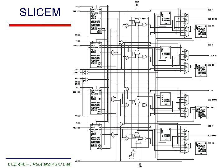
SLICEM ECE 448 – FPGA and ASIC Design with VHDL 28

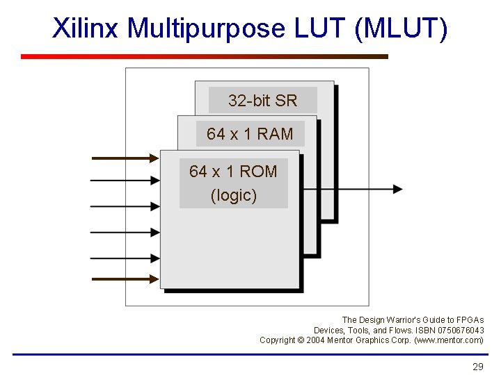
Xilinx Multipurpose LUT (MLUT) 32 -bit SR 64 x 1 RAM 64 x 1 ROM (logic) The Design Warrior’s Guide to FPGAs Devices, Tools, and Flows. ISBN 0750676043 Copyright © 2004 Mentor Graphics Corp. (www. mentor. com) 29

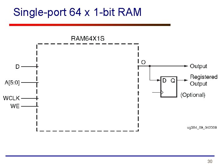
Single-port 64 x 1 -bit RAM 30

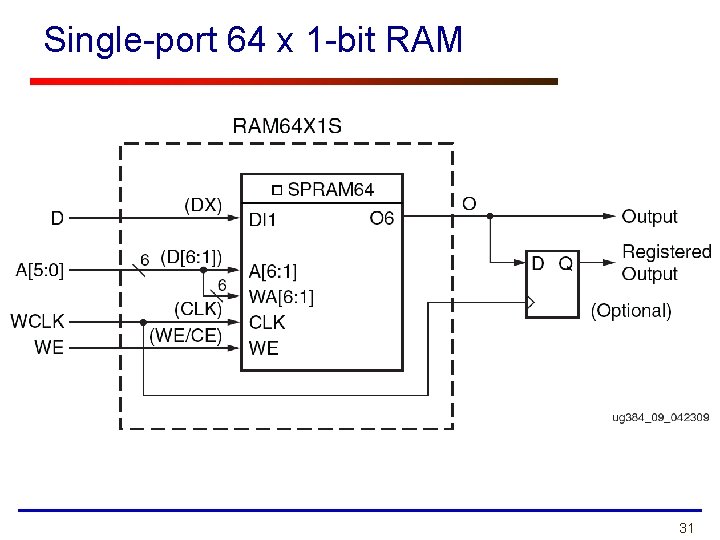
Single-port 64 x 1 -bit RAM 31

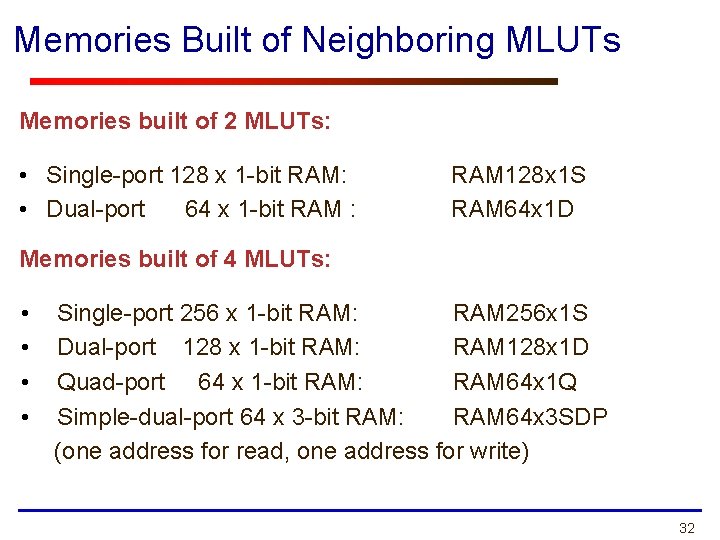
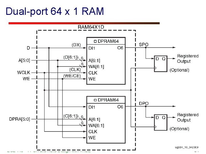
Memories Built of Neighboring MLUTs Memories built of 2 MLUTs: • Single-port 128 x 1 -bit RAM: • Dual-port 64 x 1 -bit RAM : RAM 128 x 1 S RAM 64 x 1 D Memories built of 4 MLUTs: • • Single-port 256 x 1 -bit RAM: RAM 256 x 1 S Dual-port 128 x 1 -bit RAM: RAM 128 x 1 D Quad-port 64 x 1 -bit RAM: RAM 64 x 1 Q Simple-dual-port 64 x 3 -bit RAM: RAM 64 x 3 SDP (one address for read, one address for write) 32

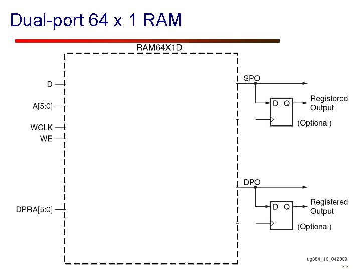
Dual-port 64 x 1 RAM • • Dual-port 64 x 1 -bit RAM : Single-port 128 x 1 -bit RAM: 64 x 1 D 128 x 1 S 33

Dual-port 64 x 1 RAM • • Dual-port 64 x 1 -bit RAM : Single-port 128 x 1 -bit RAM: ECE 448 – FPGA and ASIC Design with VHDL 64 x 1 D 128 x 1 S 34

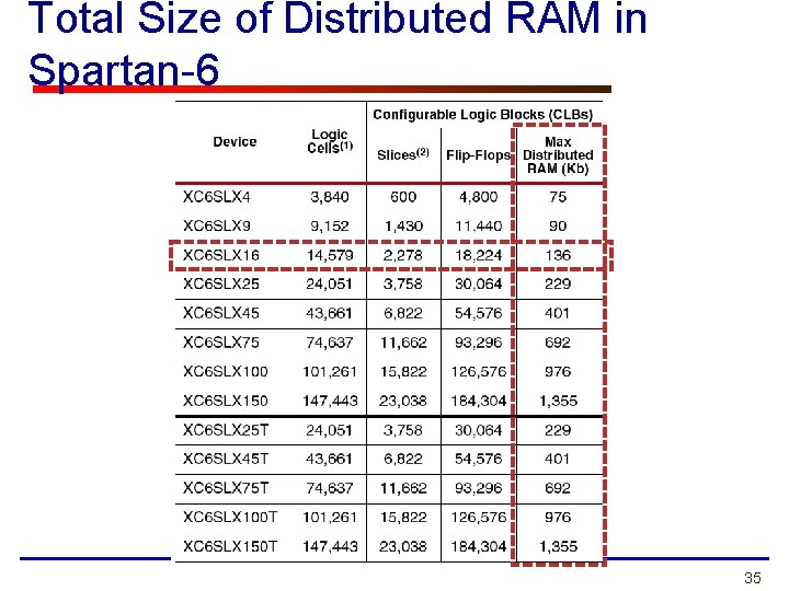
Total Size of Distributed RAM in Spartan-6 35

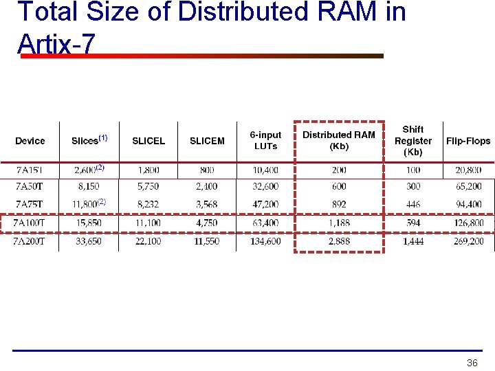
Total Size of Distributed RAM in Artix-7 36

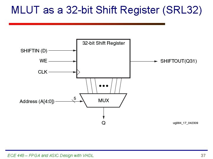
MLUT as a 32 -bit Shift Register (SRL 32) ECE 448 – FPGA and ASIC Design with VHDL 37

Input/Output Blocks (IOBs) ECE 448 – FPGA and ASIC Design with VHDL George Mason University

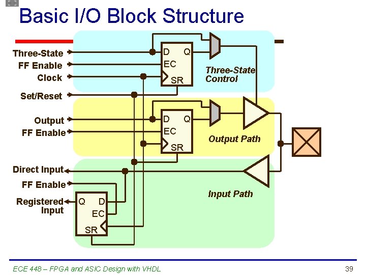
Basic I/O Block Structure D Q EC Three-State FF Enable Clock SR Three-State Control Set/Reset D Q EC Output FF Enable SR Output Path Direct Input FF Enable Registered Input Q D EC Input Path SR ECE 448 – FPGA and ASIC Design with VHDL 39

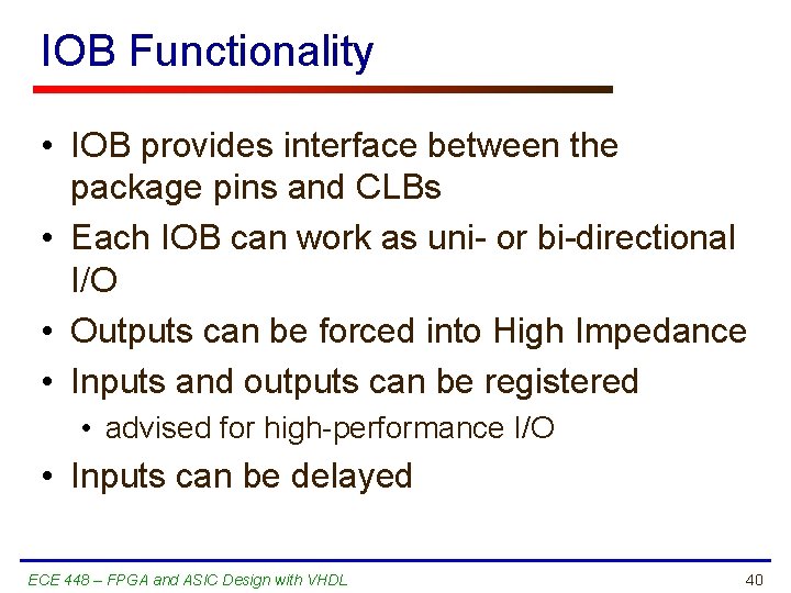
IOB Functionality • IOB provides interface between the package pins and CLBs • Each IOB can work as uni- or bi-directional I/O • Outputs can be forced into High Impedance • Inputs and outputs can be registered • advised for high-performance I/O • Inputs can be delayed ECE 448 – FPGA and ASIC Design with VHDL 40

Family Attributes ECE 448 – FPGA and ASIC Design with VHDL George Mason University

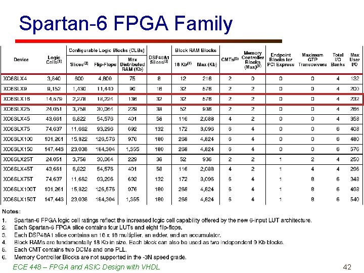
Spartan-6 FPGA Family ECE 448 – FPGA and ASIC Design with VHDL 42

Artix-7 FPGA Family ECE 448 – FPGA and ASIC Design with VHDL 43

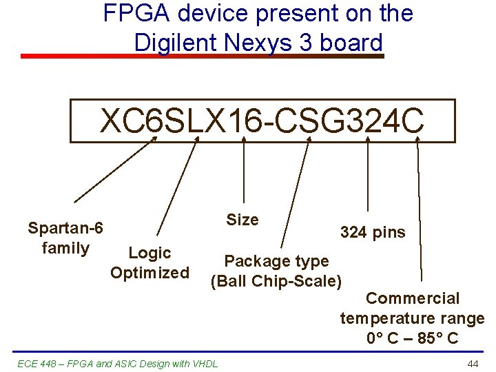
FPGA device present on the Digilent Nexys 3 board XC 6 SLX 16 -CSG 324 C Spartan-6 family Size Logic Optimized 324 pins Package type (Ball Chip-Scale) Commercial temperature range 0° C – 85° C ECE 448 – FPGA and ASIC Design with VHDL 44

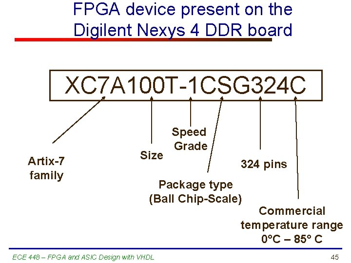
FPGA device present on the Digilent Nexys 4 DDR board XC 7 A 100 T-1 CSG 324 C Artix-7 family Size Speed Grade 324 pins Package type (Ball Chip-Scale) Commercial temperature range 0°C – 85° C ECE 448 – FPGA and ASIC Design with VHDL 45