Timing Issues Mohammad Sharifkhani Reading Textbook II Chapter

Timing Issues Mohammad Sharifkhani

Reading • Textbook II, Chapter 10 • Textbook I, Chapters 12 and 13

Motivation • Time is the essence! – We do things in order, do does the processors • Procedural dependency • Resource Reusability • Synchronous architectures are preferred – Ease of implementation – Predictability – Compatibility with well known arithmetic algorithms • A reference clock plays a key role – We usually neglect the non-idealities in the clock in the design cycle

Timinng

Clock frequency

Two signals Signals that can only transition at predetermined times with respect to a signal clock are called “{syn, meso, plesio}chronous” An asynchronous signal can transition at any arbitrary time.

Definitions data passed between two different clock domains

Mesochronous Timing

Mesochronous Timing unknown interconnect delay

Pelsichronous • two interacting modules have independent clocks generated from separate crystal oscillators

Asynchronous Interconnect • No clock is needed • Speed is determined by job completion

Hand Shaking • The four-phase handshake is level-sensitive while the twophase handshake is edgetriggered (lower transitions at the expense of edge triggered circuitry). • System A places data on the bus. It then raises Req to indicate that the data is valid. • System B samples the data when it sees a high value on Req and raises Ack to indicate that the data has been captured. System A lowers Req, then system B lowers Ack. Req is not synch to clk. B synchronizer is needed
")
Hand Shaking (Cont’)

Synchronous Timing

A quick look

Timing Definitions and Basics

Latch Parameters Transparent Opaque T Clk PWm D Q tsu thold tc-q td-q Delays can be different for rising and falling data transitions

Register Parameters T Clk thold D tsu Q tc-q Delays can be different for rising and falling data transitions

Clock Uncertainties Sources of clock uncertainty

Clock Nonidealities • Clock skew – Spatial variation in temporally equivalent clock edges; deterministic + random, t. SK • Clock jitter – Temporal variations in consecutive edges of the clock signal; modulation + random noise – Cycle-to-cycle (short-term) t. JS – Long term t. JL • Variation of the pulse width – Important for level sensitive clocking

Clock Skew and Jitter Clk t. SK Clk t. JS • Both skew and jitter affect the effective cycle time • Only skew affects the race margin

Clock Skew and Jitter Clk t. SK Clk t. JS • Do not touch the clock signal if not necessary! – Sometimes the simplest architecture is the safest – But not necessarily the lowest power!

Clock skew and Jitter • Data and state independent clock distribution is desired • Enabled FF is a popular choice in the design • Consider clock load on power!

Clock Skew # of registers Earliest occurrence of Clk edge Nominal – /2 Latest occurrence of Clk edge Nominal + /2 Insertion delay Max Clk skew Clk delay

Positive and Negative Skew

Positive Skew Launching edge arrives before the receiving edge

Negative Skew Receiving edge arrives before the launching edge
 Minimum cycle time: T + > tc-q + tsu +")
Timing Constraints (positive skew) Minimum cycle time: T + > tc-q + tsu + tlogic More time to process the data Worst case is when receiving edge arrives early (positive )
 1 Hold time constraint: t(c-q, cd) + t(logic, cd) >")
Timing Constraints (positive skew) 1 Hold time constraint: t(c-q, cd) + t(logic, cd) > thold + Otherwise it can not latch In 1 before it changes after CLK 1 edge Worst case is when receiving edge arrives late Race between data and clock (positive skew) < t(c-q, cd) + t(logic, cd) > thold independent of the T

Considerations • δ > 0—This corresponds to a clock routed in the same direction as the flow of the data through the pipeline. The skew has to be strictly controlled. If this constraint is not met, the circuit does malfunction independent of the clock period.

Question • Would there be any race if the skew is negative? • What would you do to avoid race?

Negative Skew • δ < 0—When the clock is routed in the opposite direction of the data , the skew is negative and condition to avoid race is unconditionally met. The circuit operates correctly independent of the skew. The skew reduces the time available for actual computation so that the clock period, T, has to be increased by |δ|. If race (hold time) is a problem, route the clock in the opposite direction

Impact of Jitter Both skew and jitter should be accounted for in feedback structures

Longest Logic Path in Edge-Triggered Systems TSU Clk TClk-Q Latest point of launching considering jitter TLM T Earliest arrival of next cycle TJI +

Clock Constraints in Edge-Triggered Systems If launching edge is late and receiving edge is early, the data will not be too late if: Tc-q + TLM + TSU < T – TJI, 1 – TJI, 2 - Minimum cycle time is determined by the maximum delays through the logic Tc-q + TLM + TSU + + 2 TJI < T Skew can be either positive or negative

Shortest Path Earliest point of launching Clk TClk-Q TLm TH Nominal clock edge Data must not arrive before this time

Clock Constraints in Edge-Triggered Systems If launching edge is early and receiving edge is late: Tc-q + TLM – TJI, 1 > TH + TJI, 2 + Minimum logic delay Tc-q + TLM > TH + 2 TJI+
 never exercised. If A = 1, the critical")
False path Path 1 (5 tgate) never exercised. If A = 1, the critical path goes through OR 1 and OR 2. If A = 0 and B = 0, the critical path is through I 1, OR 1 and OR 2 (corresponding to a delay of 3 tgate). For the case when A= 0 and B =1, the critical path is through I 1, OR 1, AND 3 and OR 2. Does not depend on C, D.

How to counter Clock Skew?

Sources of uncertainity

Device variation • Variation • Matching – Poly orientation – Dopant profiles • Can be modeled and compensated for
")
Interconnect variation (ILD)

Pattern and ILD correlation Use of fillers is necessary
 – Effect of clock gating")
Temp. and Power • Temp. – Time varying (milisecond) – Effect of clock gating – Has a gradient systematic compensated for • Power – Instantaneous IR Drop (switching activity) – Jitter (short pulses, data dependent) – Can not be compensated for (only decoupling caps)

Data dependent loading Capacitive coupling and X-talk works the same way. It is modeled as a form of jitter due to its random nature

Clock Distribution H-tree Clock is distributed in a tree-like fashion

Example • Clock H-Tree – Clock skew: time difference between the arrival time of the clock signal between two leaves – Identical branches and leaves

Example • Considering three parameters: – Both FETs and wires; 64 samples + main buffer – All deterministic factors are nulled out only within chip variation is considered – Random ΔL of FET with distribution stat: N(0, 0. 035 um) – Random ΔW of wires with N(0, 0. 25 um) – Spatial ΔL; ΔL = w 0+wx. x+wy. y

Example

Example • Results – In case of Random ΔL 139 ps vs. 171 ps without considering spatial constraints – In case of Random ΔW 41 ps vs. 49 ps – Without considering spatial constraints; worst case is too pessimistic

More realistic H-tree 10 Balanced segments Each segments contain 580 drivers All-RC matched If we leave Clock Tree for last minute we may end-up with multiple timing constraints violations! [Restle 98]

The Grid System Absolute delay is minimized Allows late design changes • No rc-matching • Large power
 200 MHz • Clock load 3. 25")
Examples • Alpha 21064 (0. 75 um) 200 MHz • Clock load 3. 25 n. F (40%) • Skew < 200 p. Sec (10%)

Example: DEC Alpha 21164

21164 Clocking tcycle= 3. 3 ns trise = 0. 35 ns • 2 phase single wire clock, distributed globally tskew = 150 ps • 2 distributed driver channels Clock waveform final drivers pre-driver Location of clock driver on die – – Reduced RC delay/skew Improved thermal distribution 3. 75 n. F clock load 58 cm final driver width • Local inverters for latching • Conditional clocks in caches to reduce power • More complex race checking • Device variation • Skew: 90 p. Sec (65 p. Sec effective)

21164 Clocking • Clock buffers carefully sized to minimize the skew • The direction of the clock is considered • One gate between the latches • Dummy fillers (increase cap) – Dummies are shielded

Reducing Skew • • • 1. balance clock paths from a central distribution source to individual clocking elements using H-tree structures 2. The use of local clock grids (instead of routed trees) can reduce skew at the cost of increased capacitive load and power dissipation. 3. If data dependent clock load variations causes significant jitter, differential registers that have a data independent clock load should be used. – The use of gated clocks to save also results in data dependent clock load and increased jitter. In clock networks where the fixed load is large (e. g. , using clock grids), the data dependent variation might not be significant. • 4. If data flows in one direction, route data and clock in opposite directions. This eliminates races at the cost of performance. • 5. shielding clock wires from adjacent signal wires • 6. ILD: Dummy fills • 7. Temperature: delay locked loops as discussed later in this chapter can easily compensate for temperature variations. • 8. Power supply variation : on-chip decoupling capacitors. Unfortunately, decoupling capacitors require a significant amount of area and efficient packaging solutions must be leveraged to reduce chip area.

Clock Skew in Alpha Processor
 Clocking 600 MHz – 0. 35 micron CMOS tcycle= 1.")
EV 6 (Alpha 21264) Clocking 600 MHz – 0. 35 micron CMOS tcycle= 1. 67 ns trise = 0. 35 ns Global clock waveform tskew = 50 ps • 2 Phase, with multiple conditional buffered clocks – 2. 8 n. F clock load – 40 cm final driver width • Local clocks can be gated “off” to save power • Reduced load/skew • Reduced thermal issues • Multiple clocks complicate race checking

21264 Clocking Hierarchical clocking Trade-off between power and skew Flexibility in types of clocks at each reagion Not shielded

EV 6 Clock Results ps 5 10 15 20 25 30 35 40 45 50 ps 300 305 310 315 320 325 330 335 340 345 GCLK Skew GCLK Rise Times (at Vdd/2 Crossings) (20% to 80% Extrapolated to 0% to 100%)

EV 7 Clock Hierarchy Active Skew Management and Multiple Clock Domains + widely dispersed drivers + DLLs compensate static and lowfrequency variation + divides design and verification effort - DLL design and verification is added work + tailored clocks

Latch based timing • We can have comb. Circuits between the two latches of a FF – More flexibility in terms of timing

Flip-Flop – Based Timing Skew f Logic delay TSU Flip -flop f=0 Logic Representation after M. Horowitz, VLSI Circuits 1996. Flip-flop delay TClk-Q f=1

Latch timing When data arrives to transparent latch t. D-Q D Q Latch is a ‘soft’ barrier Clk t. Clk-Q When data arrives to closed latch Data has to be ‘re-launched’

Single-Phase Clock with Latches f Latch Logic Tskl Clk Tskl Tskt latch transparent PW P

Preventing late arrivals Case 1: - The LM can start ahead of time - c 2 q limits Case 2: d 2 q limits Lgk can still operate

Preventing late arrivals

Preventing Premature Arrivals Data should not pass through the latch more than once during its transparent mode Otherwise the data loops within the transparent window of time

Single latch timing

Latch-Based Design L 1 latch is transparent when f = 0 L 1 Latch L 2 latch is transparent when f = 1 f Logic L 2 Latch

Latch-Based Timing Skew Static logic f L 1 Latch Logic Path 1 L 2 trans. L 1 latch Logic Can tolerate skew! L 2 latch f=1 L 2 Latch L 1 trans. f=0 Long Path 1 Hits L 2 transparent goes through L 2 Short Path 1 Hits L 2 latch has to wait till L 2 becomes transparent

Latch based timing Trans. when high Trans. when low
 kicks to")
Slack-borrowing Trans. when high tpd. A tpd. B CLB_B starts before (3) kicks to latch its input. ie, since CLB_A finished earlier than (3), the extra time is passed to CLB_B again e is valid before (4) to latch the input of the next CLB

Example T=125 L 4 Becomes transp. at edge no problem when exactly f arrives

Design consideration Hold time violation Data available for CLL If the falling edge of clk 2 comes with too much skew, THL might not be able to latch the previous data because of hold time violation (ie, D 2 is overwritten too quickly after the edge)

Domino logic with delays

Clock skew

No time slack borrowing

Skew tolerant domino Can we borrow time?

Multiphase

Time borrowing is possible
 Acts as completion")
Self-timed and Asynchronous Design Functions of clock in synchronous design 1) Acts as completion signal 2) Ensures the correct ordering of events Truly asynchronous design 1) Completion is ensured by careful timing analysis 2) Ordering of events is implicit in logic Self-timed design 1) Completion ensured by completion signal 2) Ordering imposed by handshaking protocol

Synchronous Pipelined Datapath What clock does is that: 1 - physical timing constraints are met 2 - Clock events serve as a logical ordering mechanism for the global system events If we guarantee these two items, we can remove the clock: -power, area, complexity of clock tree…

Synch. design • It assumes that all clock events or timing references happen simultaneously over the complete circuit. This is not the case in reality, because of effects such as clock skew and jitter. • significant current flows over a very short period of time • linking of physical and logical constraints has some obvious effects (e. g. throughput)

Self-Timed Pipelined Datapath Hand shaking blocks The logical ordering of the operations is What each signal does? ensured by the acknowledge-request scheme, often called a handshaking protocol.

Asynch. properties • Timing signals are generated locally… no high precision clock distribution over the chip (skew, etc) • Separating the physical and logical ordering Performance (data dependency and no worst case design) • The automatic shut-down of blocks that are not in use can result in power savings. (power) • Robust to variations in manufacturing and operating conditions such as temperature.

Completion Signal Generation

Completion Signal Generation

Completion Signal in DCVSL VDD B 0 Start B 1 B 0 B 1 In 2 PDN Start PDN Done

Self-Timed Adder

Completion Signal Using Current Sensing Data independent reference! Minimum delay

Hand-Shaking Protocol Two Phase Handshake The four events, data change, request, data acceptance, acknowledge proceed in a cyclic order. Every transition means that the action is valid!

Event Logic – The Muller-C Element Seq. element

2 -Phase Handshake Protocol Start from Data. Ready, Ack=0, 0. when go to 1, 0 , Req=1. The C-element is blocked (and locked), and no new data is sent to the data bus (Req stays high) as long as the transmitted data is not processed by the receiver, no matter what Data. Ready is. Advantage : FAST - minimal # of signaling events (important for global interconnect) Disadvantage : requires the detection of transitions that may occur in either direction initialization is important

Problem: Self-timed FIFO All 1 s or 0 s -> pipeline empty Alternating 1 s and 0 s -> pipeline full

2 -Phase Protocol

Example Assume there is a register at the input which loads the data at the beginning of Eval phase From [Horowitz]

Example Data. Ready 1 is asserted. Req to the second block is asserted, First C-element is locked. The second block loads data and starts the evaluation process.

Example Data. Ready 2 is asserted. Req to the third block is asserted, Second C-element is locked. The third block loads data and starts the evaluation process. The first C-element is released. Can accept a Data. Ready from the previous stage. (If Req has already come, the first Req is unleashed and goes to eval phase. )

Example

4 -Phase Handshake Protocol Also known as RTZ Slower, but unambiguous

Problem: 4 -Phase Handshake Protocol Implementation using Muller-C elements
")
Example Latches: positive edge-triggered or a levelsensitive implementation (latch when level=1)

Self-Resetting Logic Post-charge logic Self- reseting

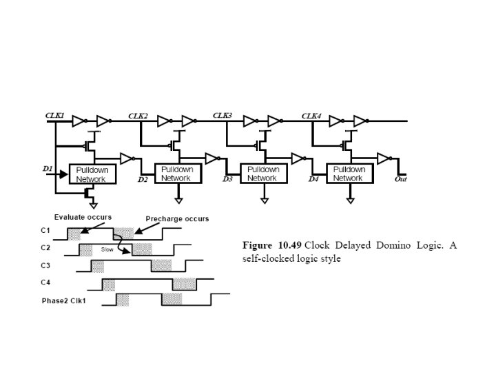
Clock-Delayed Domino This is a style of dynamic logic, where there is no global clock signal. Instead, the clock for one stage is derived from the previous stage.

Asynchronous-Synchronous Interface

Synchronizers and Arbiters • Arbiter: Circuit to decide which of 2 events occurred first • Synchronizer: Arbiter with clock f as one of the inputs • Problem: Circuit HAS to make a decision in limited time - which decision is not important • Caveat: It is impossible to ensure correct operation • But, we can decrease the error probability at the expense of delay

A Simple Synchronizer • Data sampled on rising edge of the clock • Latch will eventually resolve the signal value, but. . . this might take infinite time!

Synchronizer: Output Trajectories Single-pole model for a flip-flop

Mean Time to Failure

Example

Influence of Noise Low amplitude noise does not influence synchronization behavior

Typical Synchronizers 2 phase clocking circuit Using delay line

Cascaded Synchronizers Reduce MTF

Arbiters

PLL-Based Synchronization

PLL Block Diagram

Phase Detector Output before filtering Transfer characteristic

Phase-Frequency Detector

PFD Response to Frequency

PFD Phase Transfer Characteristic

Charge Pump

PLL Simulation
 f. REF Phase Det U")
Clock Generation using DLLs Delay-Locked Loop (Delay Line Based) f. REF Phase Det U D Charge Pump DL Filter f. O Phase-Locked Loop (VCO-Based) f. REF U ÷N PD D CP VCO Filter f. O

Delay Locked Loop

DLL-Based Clock Distribution
- Slides: 129