Interconnects Mohammad Sharifkhani With special thanks to Jan

![Structured Predictable Interconnect Example: Dense Wire Fabric ([Sunil Kathri]) Trade-off: • Cross-coupling capacitance 40 Structured Predictable Interconnect Example: Dense Wire Fabric ([Sunil Kathri]) Trade-off: • Cross-coupling capacitance 40](https://slidetodoc.com/presentation_image/3259c18c1ec3c24ce673748e595cd527/image-13.jpg)
- Slides: 80

Interconnects Mohammad Sharifkhani With special thanks to Jan Rabaei

Reading • Textbook II, Chapter 9 – You may have to take a look at previous chapters too

Impact of Interconnect Parasitics • Reduce Robustness • Affect Performance • Increase delay • Increase power dissipation Classes of Parasitics • Capacitive • Resistive • Inductive

INTERCONNECT

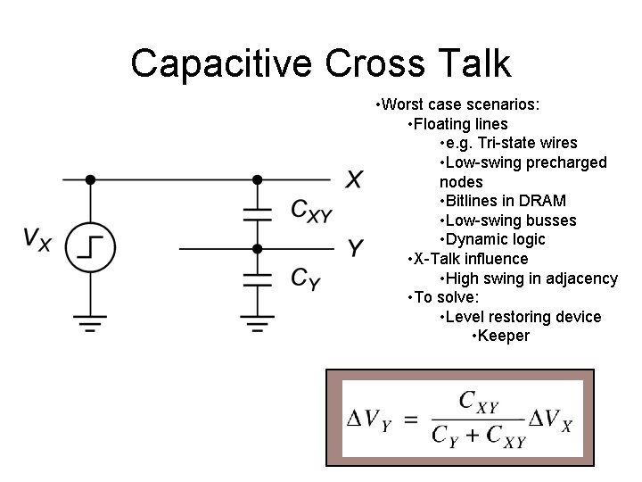
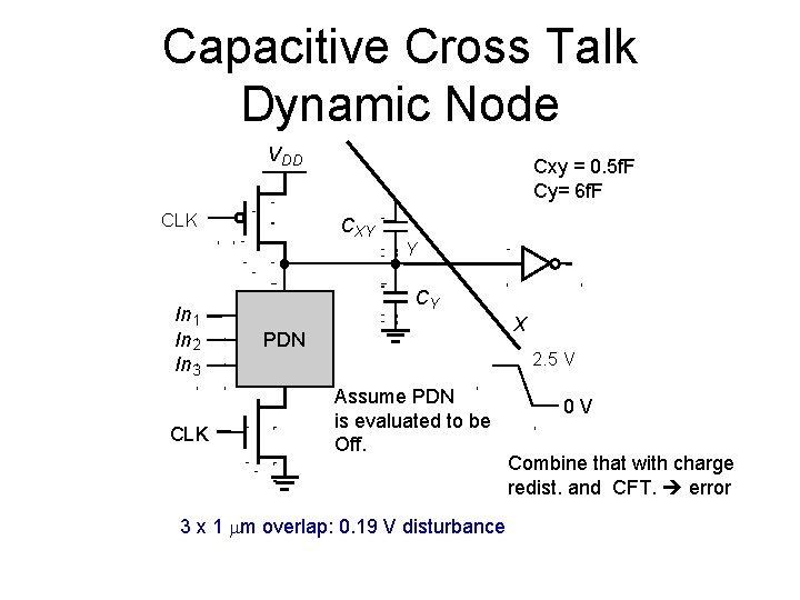
Capacitive Cross Talk • Worst case scenarios: • Floating lines • e. g. Tri-state wires • Low-swing precharged nodes • Bitlines in DRAM • Low-swing busses • Dynamic logic • X-Talk influence • High swing in adjacency • To solve: • Level restoring device • Keeper

Capacitive Cross Talk Dynamic Node V DD CLK In 1 In 2 In 3 CLK Cxy = 0. 5 f. F Cy= 6 f. F CXY Y CY X PDN 2. 5 V Assume PDN is evaluated to be Off. 3 x 1 mm overlap: 0. 19 V disturbance 0 V Combine that with charge redist. and CFT. error

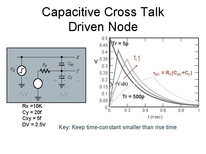
Capacitive Cross Talk Driven Node 0. 5 Tr = 5 p 0. 45 0. 4 X VX RY CXY Y CY V t r↑ 0. 35 0. 3 t. XY = RY(CXY+CY) 0. 25 0. 2 0. 15 V (Volt) 0. 1 Tr = 500 p 0. 05 Rx =10 K Cy = 20 f Cxy = 5 f DV = 2. 5 V 0 0 0. 2 0. 4 0. 6 t (nsec) Key: Keep time-constant smaller than rise time 0. 8 1

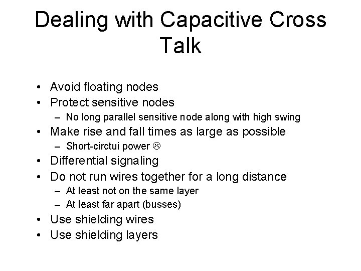
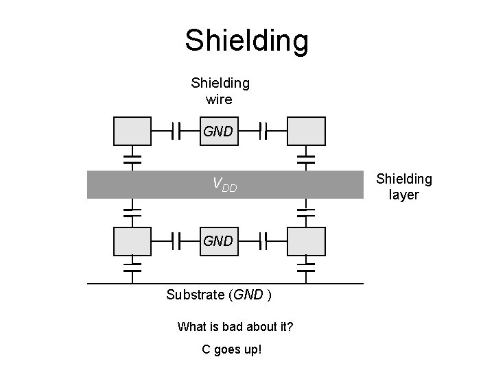
Dealing with Capacitive Cross Talk • Avoid floating nodes • Protect sensitive nodes – No long parallel sensitive node along with high swing • Make rise and fall times as large as possible – Short-circtui power • Differential signaling • Do not run wires together for a long distance – At least not on the same layer – At least far apart (busses) • Use shielding wires • Use shielding layers

Shielding wire GND V DD GND Substrate (GND ) What is bad about it? C goes up! Shielding layer

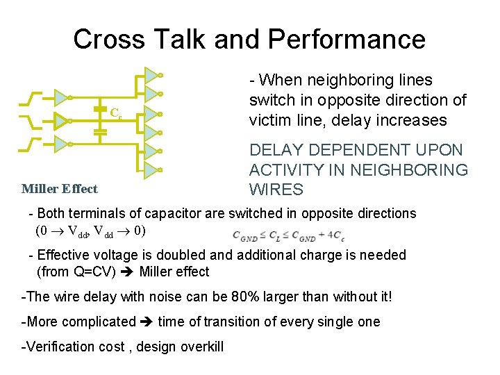
Cross Talk and Performance Cc Miller Effect - When neighboring lines switch in opposite direction of victim line, delay increases DELAY DEPENDENT UPON ACTIVITY IN NEIGHBORING WIRES - Both terminals of capacitor are switched in opposite directions (0 Vdd, Vdd 0) - Effective voltage is doubled and additional charge is needed (from Q=CV) Miller effect -The wire delay with noise can be 80% larger than without it! -More complicated time of transition of every single one -Verification cost , design overkill

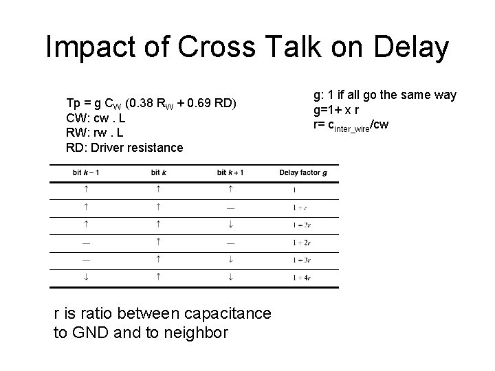
Impact of Cross Talk on Delay Tp = g CW (0. 38 RW + 0. 69 RD) CW: cw. L RW: rw. L RD: Driver resistance r is ratio between capacitance to GND and to neighbor g: 1 if all go the same way g=1+ x r r= cinter_wire/cw

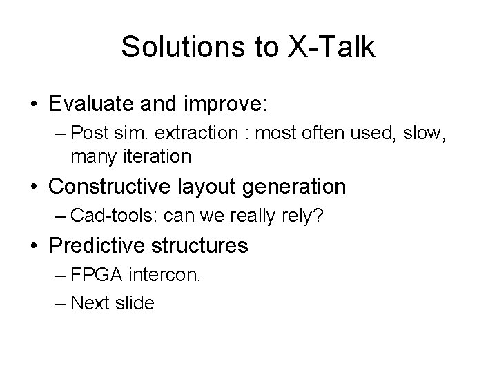
Solutions to X-Talk • Evaluate and improve: – Post sim. extraction : most often used, slow, many iteration • Constructive layout generation – Cad-tools: can we really rely? • Predictive structures – FPGA intercon. – Next slide
![Structured Predictable Interconnect Example Dense Wire Fabric Sunil Kathri Tradeoff Crosscoupling capacitance 40 Structured Predictable Interconnect Example: Dense Wire Fabric ([Sunil Kathri]) Trade-off: • Cross-coupling capacitance 40](https://slidetodoc.com/presentation_image/3259c18c1ec3c24ce673748e595cd527/image-13.jpg)
Structured Predictable Interconnect Example: Dense Wire Fabric ([Sunil Kathri]) Trade-off: • Cross-coupling capacitance 40 x lower, 2% delay variation • Increase in area and overall capacitance Also: FPGAs, VPGAs

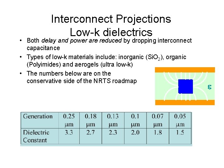
Interconnect Projections Low-k dielectrics • Both delay and power are reduced by dropping interconnect capacitance • Types of low-k materials include: inorganic (Si. O 2), organic (Polyimides) and aerogels (ultra low-k) • The numbers below are on the conservative side of the NRTS roadmap e

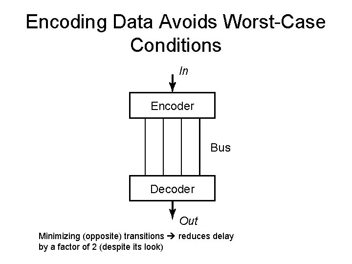
Encoding Data Avoids Worst-Case Conditions In Encoder Bus Decoder Out Minimizing (opposite) transitions reduces delay by a factor of 2 (despite its look)

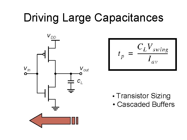
Driving Large Capacitances V DD V in V out CL • Transistor Sizing • Cascaded Buffers

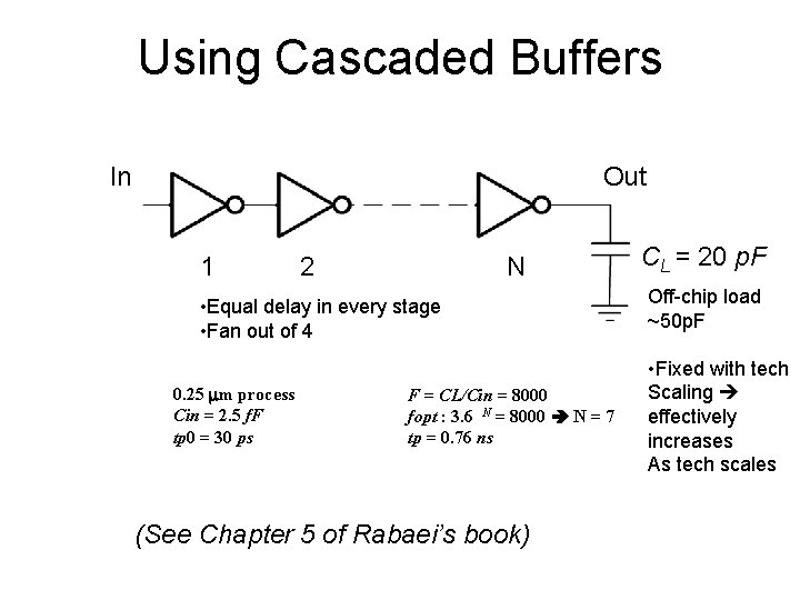
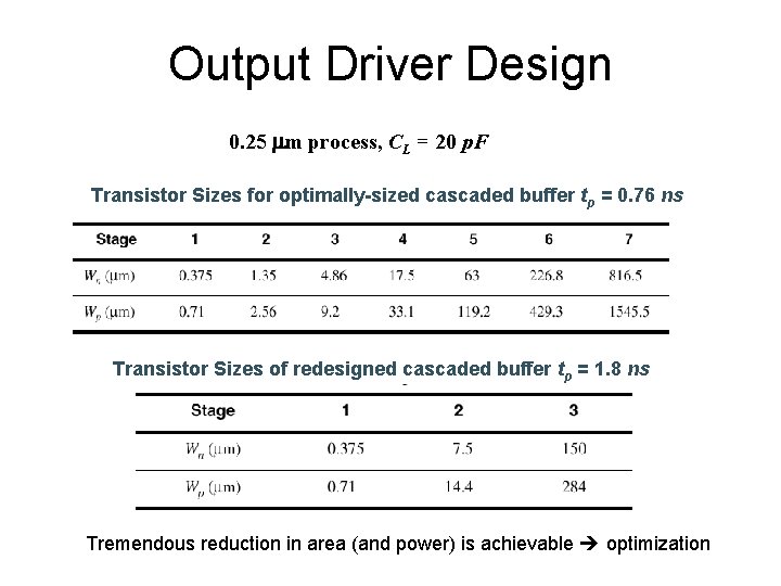
Using Cascaded Buffers In Out 1 2 N • Equal delay in every stage • Fan out of 4 0. 25 mm process Cin = 2. 5 f. F tp 0 = 30 ps F = CL/Cin = 8000 fopt : 3. 6 N = 8000 N = 7 tp = 0. 76 ns (See Chapter 5 of Rabaei’s book) CL = 20 p. F Off-chip load ~50 p. F • Fixed with tech Scaling effectively increases As tech scales

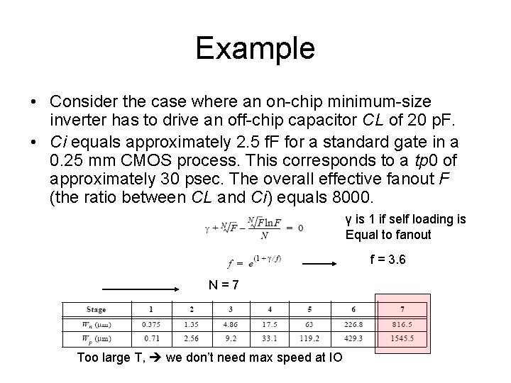
Example • Consider the case where an on-chip minimum-size inverter has to drive an off-chip capacitor CL of 20 p. F. • Ci equals approximately 2. 5 f. F for a standard gate in a 0. 25 mm CMOS process. This corresponds to a tp 0 of approximately 30 psec. The overall effective fanout F (the ratio between CL and Ci) equals 8000. γ is 1 if self loading is Equal to fanout f = 3. 6 N=7 Too large T, we don’t need max speed at IO

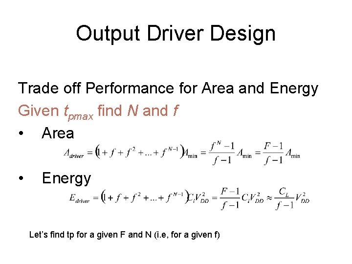
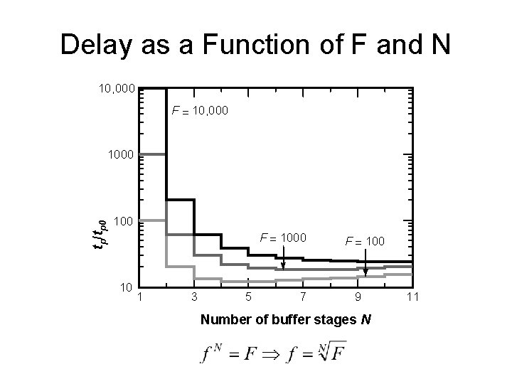
Output Driver Design Trade off Performance for Area and Energy Given tpmax find N and f • Area • Energy Let’s find tp for a given F and N (i. e, for a given f)

Delay as a Function of F and N 10, 000 F = 10, 000 tp/tp 0 100 F = 1000 10 1 3 5 7 F = 100 9 Number of buffer stages N 11

Output Driver Design 0. 25 mm process, CL = 20 p. F Transistor Sizes for optimally-sized cascaded buffer tp = 0. 76 ns Transistor Sizes of redesigned cascaded buffer tp = 1. 8 ns Tremendous reduction in area (and power) is achievable optimization

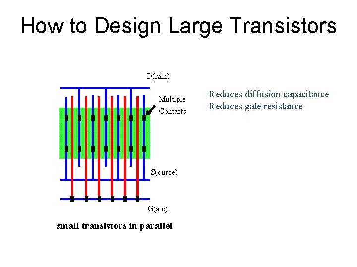
How to Design Large Transistors D(rain) Multiple Contacts S(ource) G(ate) small transistors in parallel Reduces diffusion capacitance Reduces gate resistance

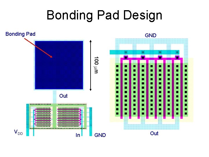
Bonding Pad Design Bonding Pad GND 100 mm Out VDD In GND Out

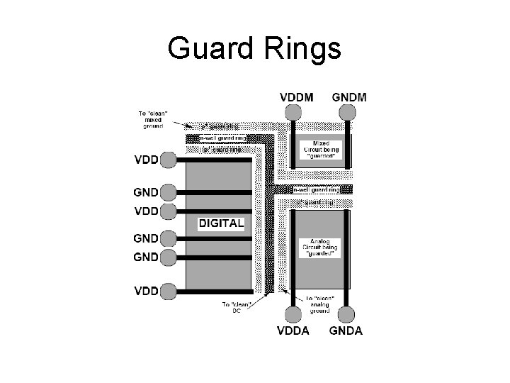
Guard Rings

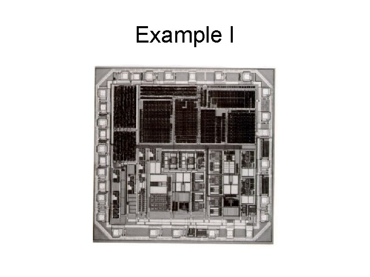
Example I

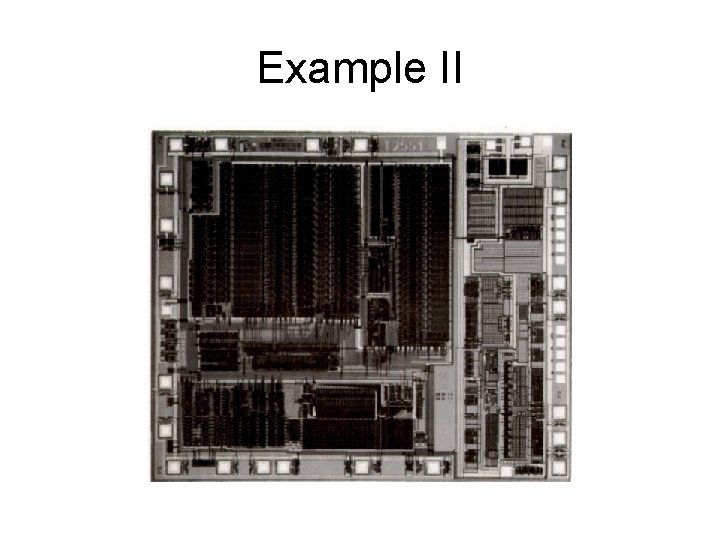
Example II

INTERCONNECT

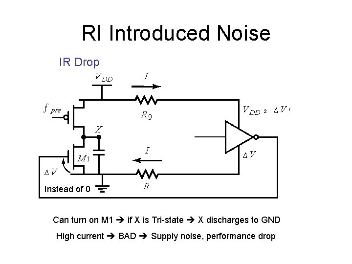
Impact of Resistance • We have already learned how to drive RC interconnect • Impact of resistance is commonly seen in power supply distribution: – IR drop – Voltage variations • Power supply is distributed to minimize the IR drop and the change in current due to switching of gates

RI Introduced Noise IR Drop V DD f pre I R 9 V DD 2 Δ V ‘ X M 1 I ΔV ΔV Instead of 0 R Can turn on M 1 if X is Tri-state X discharges to GND High current BAD Supply noise, performance drop


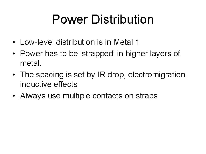
Power Distribution • Low-level distribution is in Metal 1 • Power has to be ‘strapped’ in higher layers of metal. • The spacing is set by IR drop, electromigration, inductive effects • Always use multiple contacts on straps

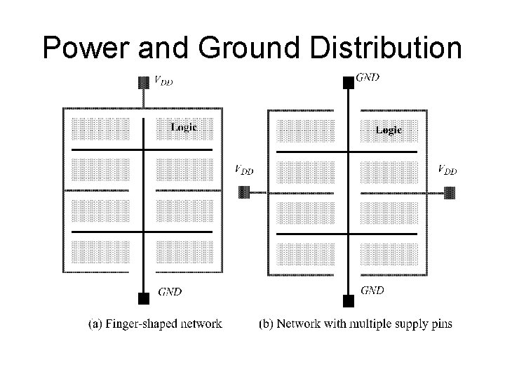
Power and Ground Distribution

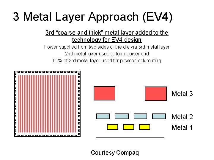
3 Metal Layer Approach (EV 4) 3 rd “coarse and thick” metal layer added to the technology for EV 4 design Power supplied from two sides of the die via 3 rd metal layer 2 nd metal layer used to form power grid 90% of 3 rd metal layer used for power/clock routing Metal 3 Metal 2 Metal 1 Courtesy Compaq

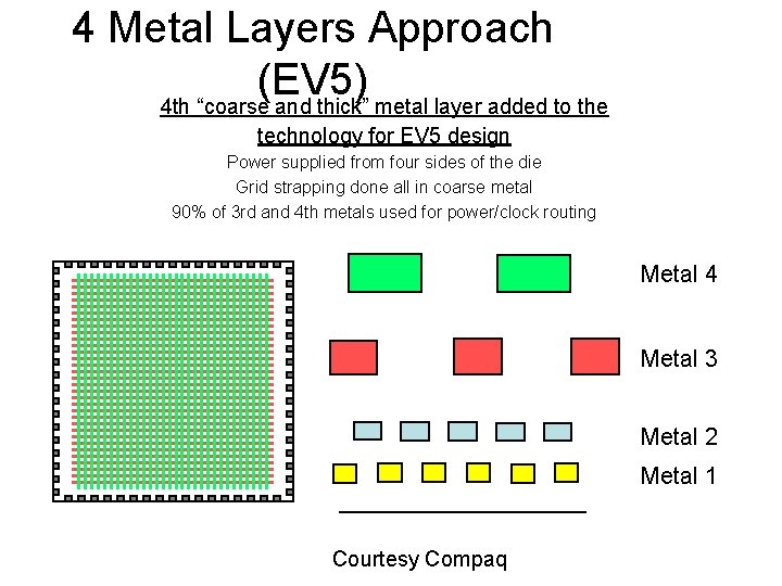
4 Metal Layers Approach (EV 5) 4 th “coarse and thick” metal layer added to the technology for EV 5 design Power supplied from four sides of the die Grid strapping done all in coarse metal 90% of 3 rd and 4 th metals used for power/clock routing Metal 4 Metal 3 Metal 2 Metal 1 Courtesy Compaq

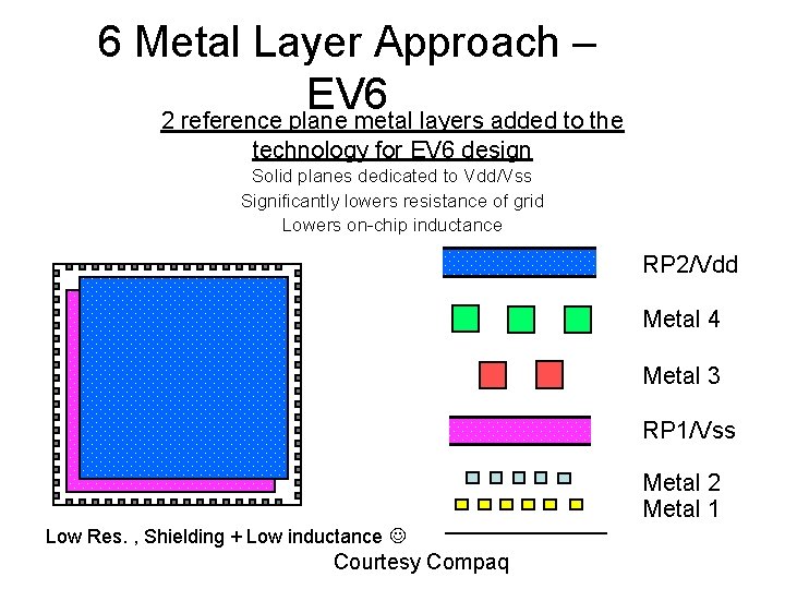
6 Metal Layer Approach – EV 6 2 reference plane metal layers added to the technology for EV 6 design Solid planes dedicated to Vdd/Vss Significantly lowers resistance of grid Lowers on-chip inductance RP 2/Vdd Metal 4 Metal 3 RP 1/Vss Metal 2 Metal 1 Low Res. , Shielding + Low inductance Courtesy Compaq

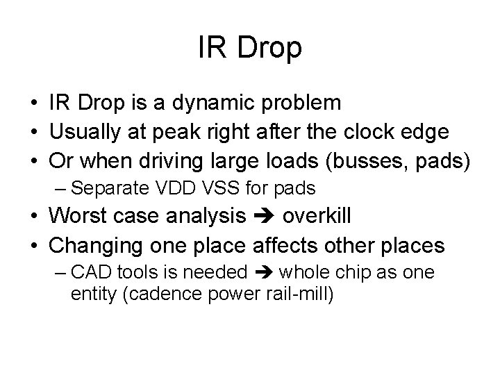
IR Drop • IR Drop is a dynamic problem • Usually at peak right after the clock edge • Or when driving large loads (busses, pads) – Separate VDD VSS for pads • Worst case analysis overkill • Changing one place affects other places – CAD tools is needed whole chip as one entity (cadence power rail-mill)

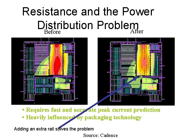
Resistance and the Power Distribution Problem After Before • Requires fast and accurate peak current prediction • Heavily influenced by packaging technology Adding an extra rail solves the problem Source: Cadence

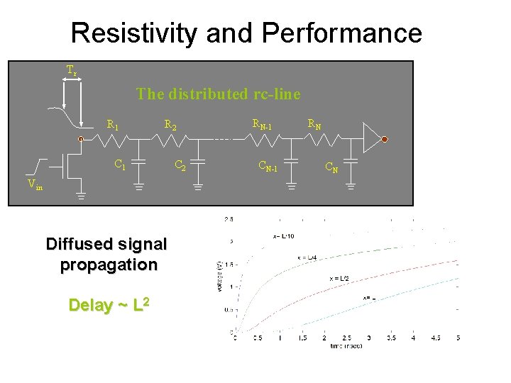
Resistivity and Performance Tr The distributed rc-line R 1 R 2 C 1 Vin Diffused signal propagation Delay ~ L 2 C 2 RN-1 CN-1 RN CN

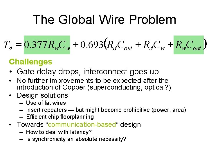
The Global Wire Problem Td = 0. 377 Rw. Cw + 0. 693(Rd Cout + Rd Cw + Rw. Cout ) Challenges • Gate delay drops, interconnect goes up • No further improvements to be expected after the introduction of Copper (superconducting, optical? ) • Design solutions – Use of fat wires – Insert repeaters — but might become prohibitive (power, area) – Efficient chip floorplanning • Towards “communication-based” design – How to deal with latency? – Is synchronicity an absolute necessity?

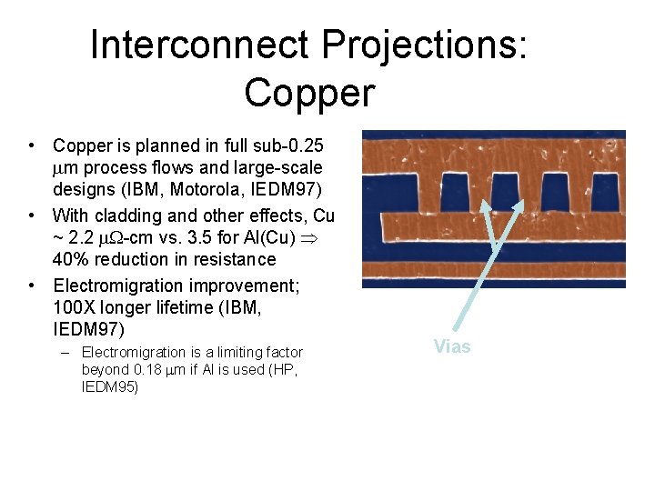
Interconnect Projections: Copper • Copper is planned in full sub-0. 25 mm process flows and large-scale designs (IBM, Motorola, IEDM 97) • With cladding and other effects, Cu ~ 2. 2 m. W-cm vs. 3. 5 for Al(Cu) 40% reduction in resistance • Electromigration improvement; 100 X longer lifetime (IBM, IEDM 97) – Electromigration is a limiting factor beyond 0. 18 mm if Al is used (HP, IEDM 95) Vias

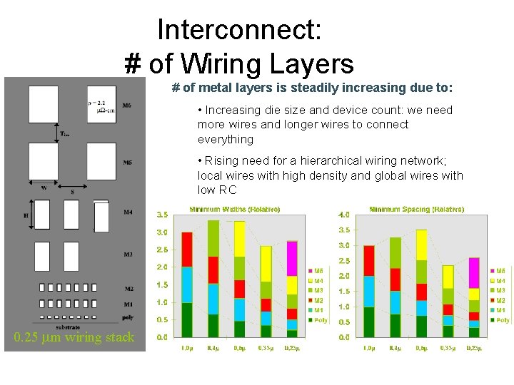
Interconnect: # of Wiring Layers # of metal layers is steadily increasing due to: • Increasing die size and device count: we need more wires and longer wires to connect everything • Rising need for a hierarchical wiring network; local wires with high density and global wires with low RC 0. 25 mm wiring stack

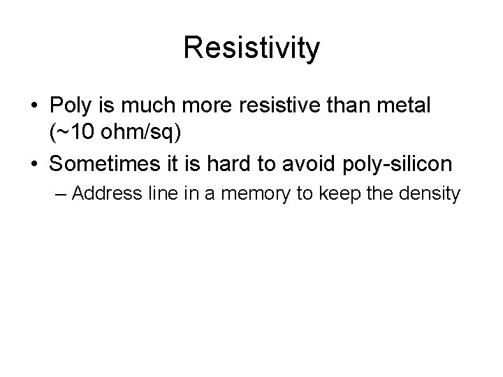
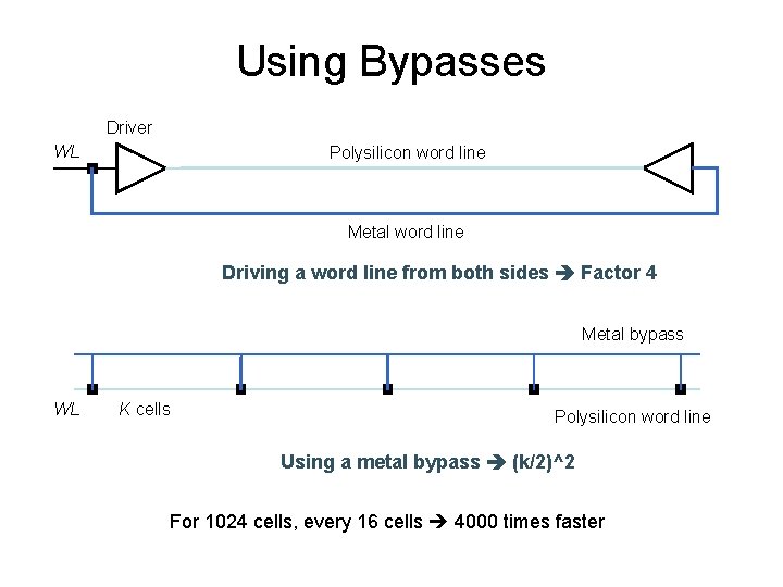
Resistivity • Poly is much more resistive than metal (~10 ohm/sq) • Sometimes it is hard to avoid poly-silicon – Address line in a memory to keep the density

Using Bypasses Driver WL Polysilicon word line Metal word line Driving a word line from both sides Factor 4 Metal bypass WL K cells Polysilicon word line Using a metal bypass (k/2)^2 For 1024 cells, every 16 cells 4000 times faster

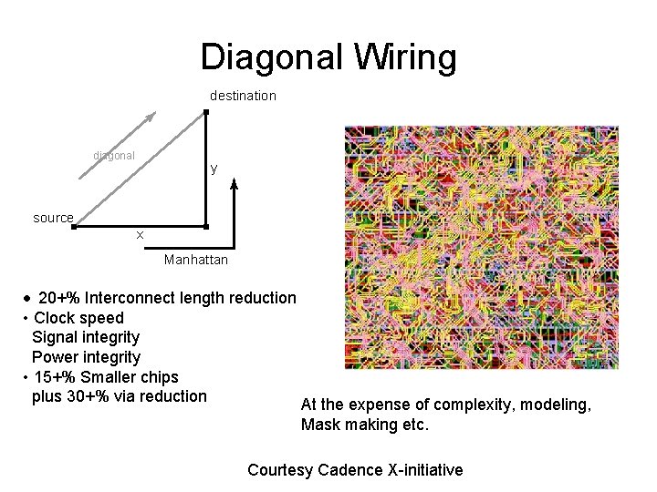
Diagonal Wiring destination diagonal y source x Manhattan • 20+% Interconnect length reduction • Clock speed Signal integrity Power integrity • 15+% Smaller chips plus 30+% via reduction At the expense of complexity, modeling, Mask making etc. Courtesy Cadence X-initiative

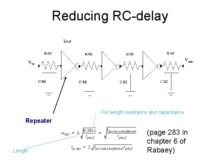
Reducing RC-delay Per length resistance and capacitance Repeater Length (page 283 in chapter 6 of Rabaey)

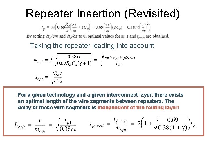
Repeater Insertion (Revisited) Taking the repeater loading into account For a given technology and a given interconnect layer, there exists an optimal length of the wire segments between repeaters. The delay of these wire segments is independent of the routing layer!

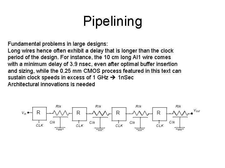
Pipelining Fundamental problems in large designs: Long wires hence often exhibit a delay that is longer than the clock period of the design. For instance, the 10 cm long Al 1 wire comes with a minimum delay of 3. 9 nsec, even after optimal buffer insertion and sizing, while the 0. 25 mm CMOS process featured in this text can sustain clock speeds in excess of 1 GHz 1 n. Sec Architectural innovations is needed

INTERCONNECT

Inductance • Important source of parasitics: – Bond wires, chip packages • High current and long inductive wires • Change on the on-chip supply – Especially output pads • Reduced logic levels noise margin

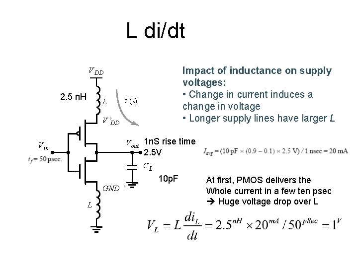
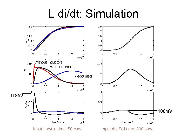
L di/dt Impact of inductance on supply voltages: • Change in current induces a change in voltage • Longer supply lines have larger L V DD 2. 5 n. H L i (t) V ’DD V out 1 n. S rise time V in 2. 5 V CL 10 p. F GND ’ L At first, PMOS delivers the Whole current in a few ten psec Huge voltage drop over L

2. 5 2 2 1. 5 out (V) L di/dt: Simulation 1 0. 5 V 1 0 0. 5 1 1. 5 2 x 10 Without inductors With inductors 0. 02 0 decoupled 0 0. 5 1 1. 5 2 x 10 -9 0. 02 0 0 0. 5 1 1. 5 -9 1 0. 5 2 0. 5 L V (V) 0. 95 V 2 x 10 1 0. 5 0. 04 L i (A) 0. 04 0 -9 0 100 m. V 0 0 0. 5 1 time (nsec) 1. 5 2 x 10 -9 Input rise/fall time: 50 psec 0 0. 5 1 time (nsec) 1. 5 2 x 10 -9 Input rise/fall time: 800 psec

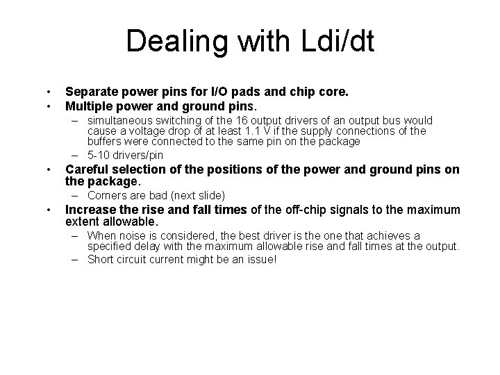
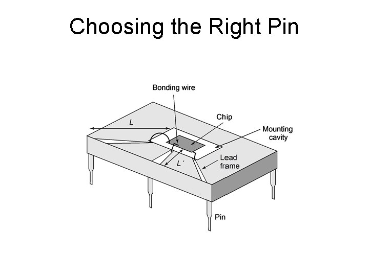
Dealing with Ldi/dt • • Separate power pins for I/O pads and chip core. Multiple power and ground pins. – simultaneous switching of the 16 output drivers of an output bus would cause a voltage drop of at least 1. 1 V if the supply connections of the buffers were connected to the same pin on the package – 5 -10 drivers/pin • Careful selection of the positions of the power and ground pins on the package. – Corners are bad (next slide) • Increase the rise and fall times of the off-chip signals to the maximum extent allowable. – When noise is considered, the best driver is the one that achieves a specified delay with the maximum allowable rise and fall times at the output. – Short circuit current might be an issue!

Choosing the Right Pin

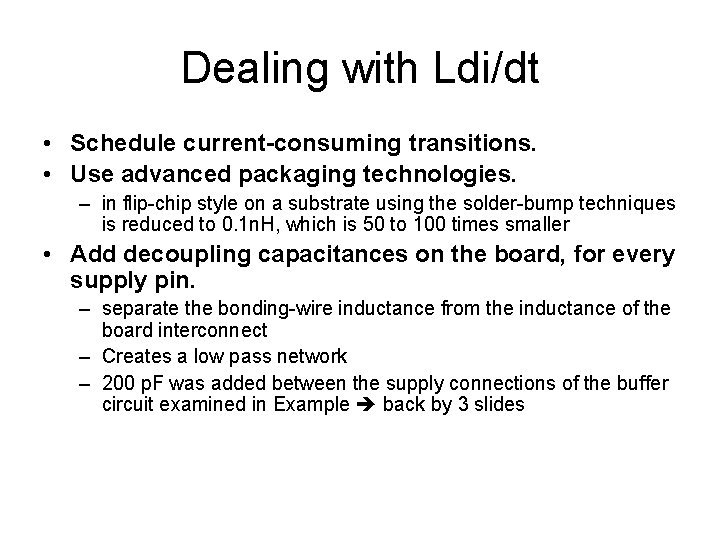
Dealing with Ldi/dt • Schedule current-consuming transitions. • Use advanced packaging technologies. – in flip-chip style on a substrate using the solder-bump techniques is reduced to 0. 1 n. H, which is 50 to 100 times smaller • Add decoupling capacitances on the board, for every supply pin. – separate the bonding-wire inductance from the inductance of the board interconnect – Creates a low pass network – 200 p. F was added between the supply connections of the buffer circuit examined in Example back by 3 slides

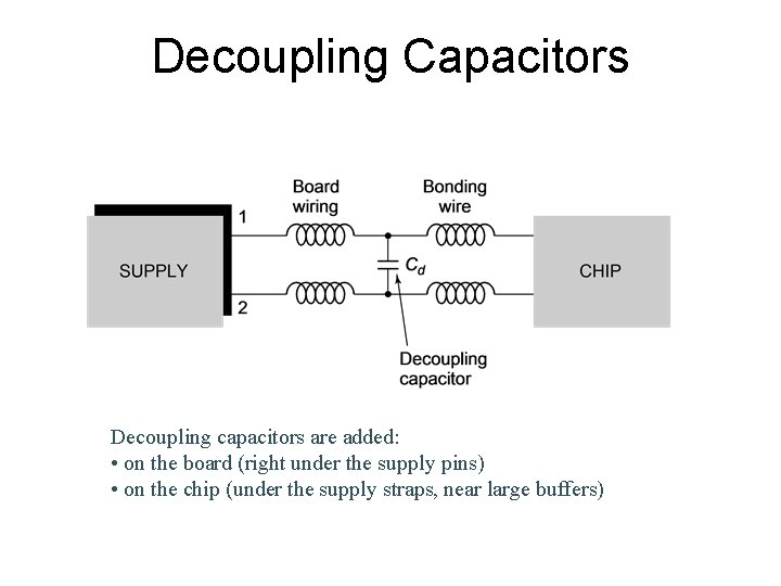
Decoupling Capacitors Decoupling capacitors are added: • on the board (right under the supply pins) • on the chip (under the supply straps, near large buffers)

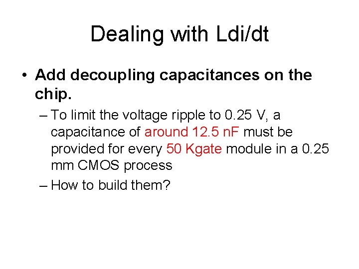
Dealing with Ldi/dt • Add decoupling capacitances on the chip. – To limit the voltage ripple to 0. 25 V, a capacitance of around 12. 5 n. F must be provided for every 50 Kgate module in a 0. 25 mm CMOS process – How to build them?

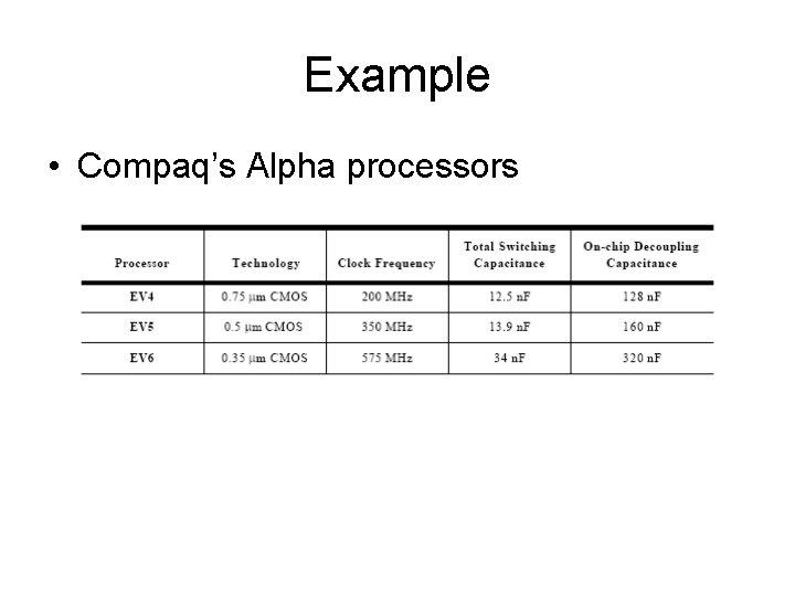
Example • Compaq’s Alpha processors

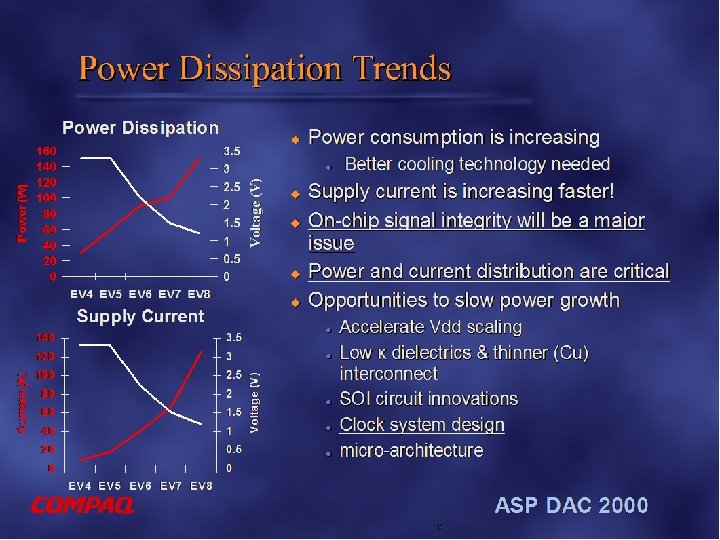
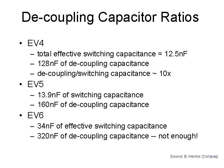
De-coupling Capacitor Ratios • EV 4 – total effective switching capacitance = 12. 5 n. F – 128 n. F of de-coupling capacitance – de-coupling/switching capacitance ~ 10 x • EV 5 – 13. 9 n. F of switching capacitance – 160 n. F of de-coupling capacitance • EV 6 – 34 n. F of effective switching capacitance – 320 n. F of de-coupling capacitance -- not enough! Source: B. Herrick (Compaq)

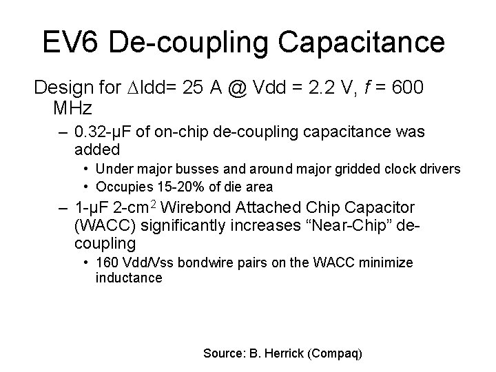
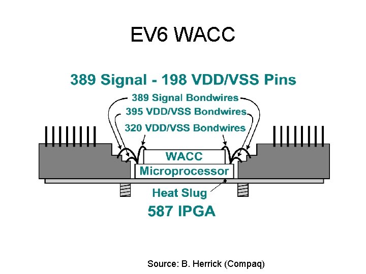
EV 6 De-coupling Capacitance Design for Idd= 25 A @ Vdd = 2. 2 V, f = 600 MHz – 0. 32 -µF of on-chip de-coupling capacitance was added • Under major busses and around major gridded clock drivers • Occupies 15 -20% of die area – 1 -µF 2 -cm 2 Wirebond Attached Chip Capacitor (WACC) significantly increases “Near-Chip” decoupling • 160 Vdd/Vss bondwire pairs on the WACC minimize inductance Source: B. Herrick (Compaq)

EV 6 WACC Source: B. Herrick (Compaq)

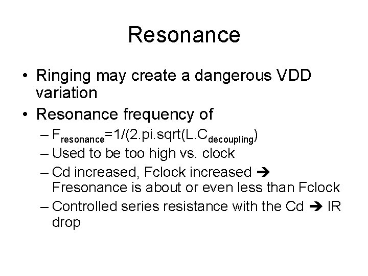
Resonance • Ringing may create a dangerous VDD variation • Resonance frequency of – Fresonance=1/(2. pi. sqrt(L. Cdecoupling) – Used to be too high vs. clock – Cd increased, Fclock increased Fresonance is about or even less than Fclock – Controlled series resistance with the Cd IR drop

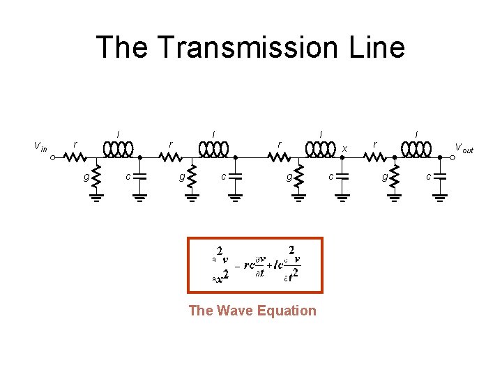
Question • What if the rise/fall time is close to the time that it takes for the signal to travel from one side of a wire to the other side? – Eg. Long enough wires – Fast switches

The Transmission Line V in l r g l r c x g The Wave Equation c l r V out g c

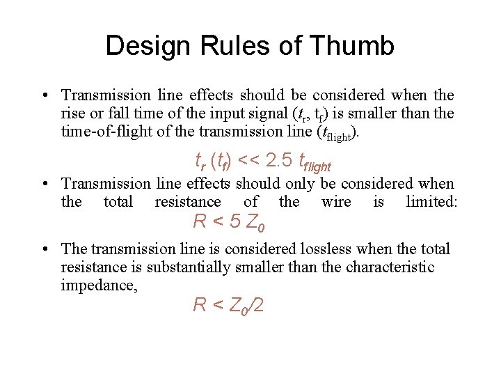
Design Rules of Thumb • Transmission line effects should be considered when the rise or fall time of the input signal (tr, tf) is smaller than the time-of-flight of the transmission line (tflight). tr (tf) << 2. 5 tflight • Transmission line effects should only be considered when the total resistance of the wire is limited: R < 5 Z 0 • The transmission line is considered lossless when the total resistance is substantially smaller than the characteristic impedance, R < Z 0/2

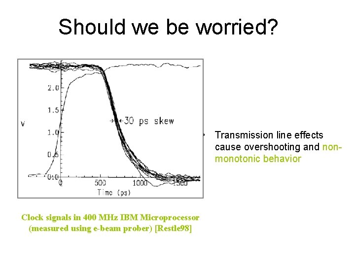
Should we be worried? • Transmission line effects cause overshooting and nonmonotonic behavior Clock signals in 400 MHz IBM Microprocessor (measured using e-beam prober) [Restle 98]

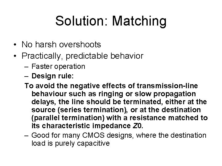
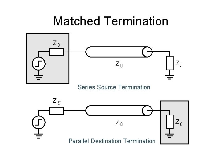
Solution: Matching • No harsh overshoots • Practically, predictable behavior – Faster operation – Design rule: To avoid the negative effects of transmission-line behaviour such as ringing or slow propagation delays, the line should be terminated, either at the source (series termination), or at the destination (parallel termination) with a resistance matched to its characteristic impedance Z 0. – Good for many CMOS designs, where the destination load is purely capacitive

Matched Termination Z 0 ZL Series Source Termination ZS Z 0 Parallel Destination Termination Z 0

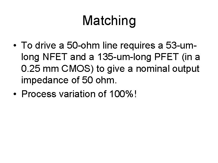
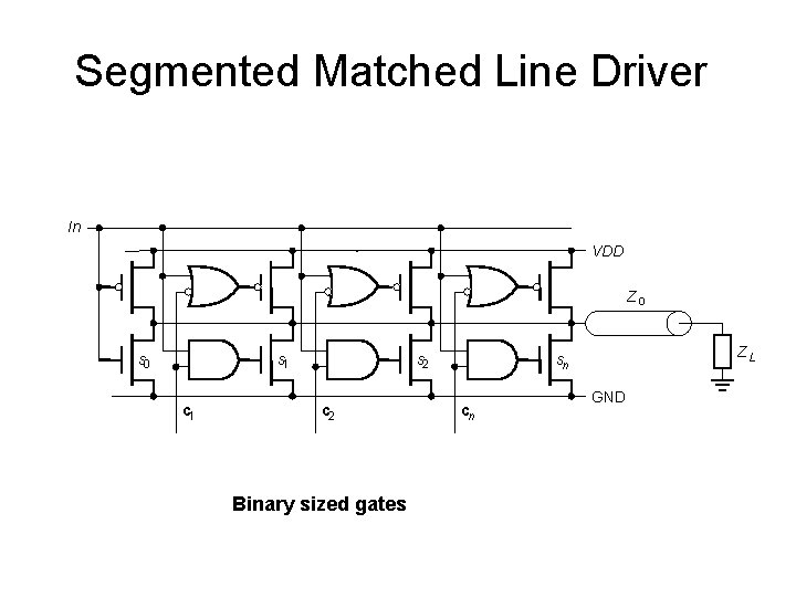
Matching • To drive a 50 -ohm line requires a 53 -umlong NFET and a 135 -um-long PFET (in a 0. 25 mm CMOS) to give a nominal output impedance of 50 ohm. • Process variation of 100%!

Segmented Matched Line Driver In VDD Z 0 s 1 c 1 s 2 c 2 Binary sized gates ZL sn cn GND

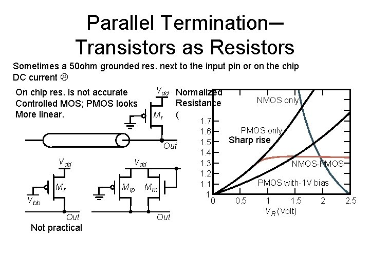
Parallel Termination─ Transistors as Resistors Sometimes a 50 ohm grounded res. next to the input pin or on the chip DC current V dd Normalized On chip res. is not accurate Controlled MOS; PMOS looks More linear. Mr Out Vdd Mr Vdd M rp M rn V bb Out Not practical NMOS only Resistance ( Out 1. 7 1. 6 1. 5 1. 4 1. 3 1. 2 1. 1 1 0 PMOS only Sharp rise NMOS-PMOS with-1 V bias 0. 5 1 1. 5 VR (Volt) 2 2. 5

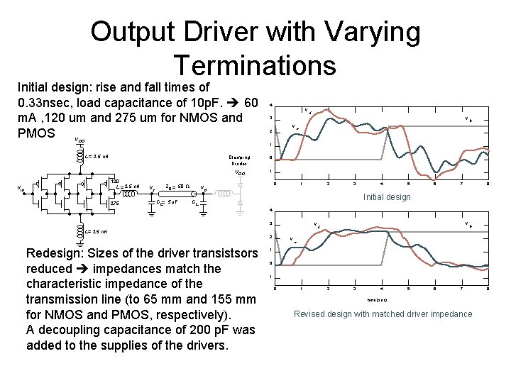
Output Driver with Varying Terminations Initial design: rise and fall times of 0. 33 nsec, load capacitance of 10 p. F. 60 m. A , 120 um and 275 um for NMOS and PMOS V DD 4 V d 3 V V 2 in s 1 L = 2. 5 n. H 120 L = 2. 5 n. H V in 275 Vs Z 0 = 50 W C L= 5 p. F Clamping Diodes 0 V DD 1 0 Vd 1 2 3 4 5 6 7 8 Initial design CL 4 3 V L= 2. 5 n. H 2 Redesign: Sizes of the driver transistsors reduced impedances match the characteristic impedance of the transmission line (to 65 mm and 155 mm for NMOS and PMOS, respectively). A decoupling capacitance of 200 p. F was added to the supplies of the drivers. V V d in s 1 0 1 2 3 4 5 6 7 time (sec) Revised design with matched driver impedance 8

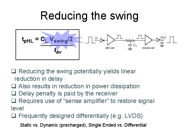
Reducing the swing q Reducing the swing potentially yields linear reduction in delay q Also results in reduction in power dissipation q Delay penalty is paid by the receiver q Requires use of “sense amplifier” to restore signal level q Frequently designed differentially (e. g. LVDS) Static vs. Dynamic (precharged), Single Ended vs. Differential

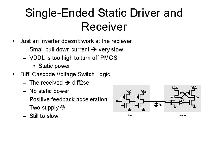
Single-Ended Static Driver and Receiver • Just an inverter doesn’t work at the reciever – Small pull down current very slow – VDDL is too high to turn off PMOS • Static power • Diff. Cascode Voltage Switch Logic – The received diff 2 se – No static power – Positive feedback acceleration – Two supply – Still to slow VDD Out In driver VDD L CL receiver Out

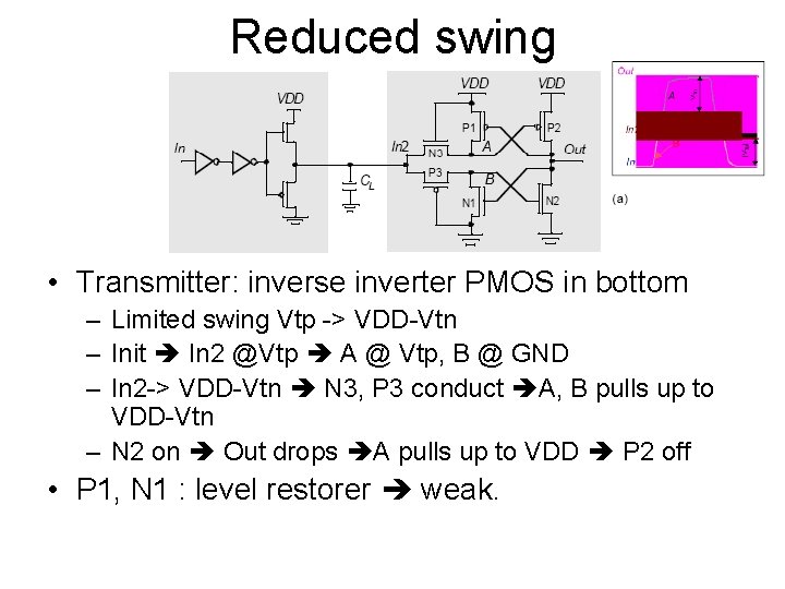
Reduced swing • Transmitter: inverse inverter PMOS in bottom – Limited swing Vtp -> VDD-Vtn – Init In 2 @Vtp A @ Vtp, B @ GND – In 2 -> VDD-Vtn N 3, P 3 conduct A, B pulls up to VDD-Vtn – N 2 on Out drops A pulls up to VDD P 2 off • P 1, N 1 : level restorer weak.

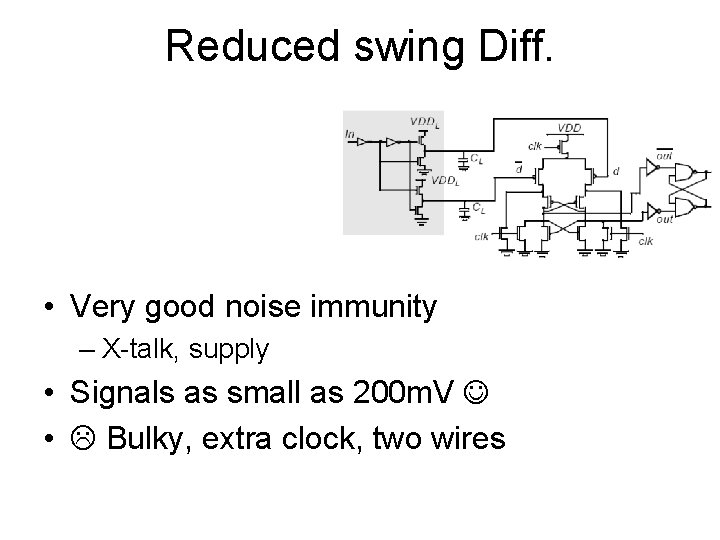
Reduced swing Diff. • Very good noise immunity – X-talk, supply • Signals as small as 200 m. V • Bulky, extra clock, two wires

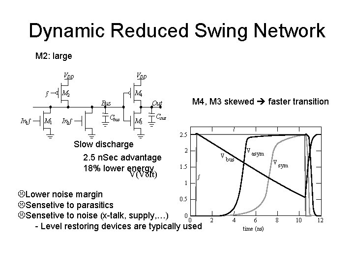
Dynamic Reduced Swing Network M 2: large f VDD M 2 M 4 Bus In 1. f M 1 In 2. f Cbus M 4, M 3 skewed faster transition Out M 3 Cout 2. 5 Slow discharge 2. 5 n. Sec advantage 18% lower energy V(Volt) 2 V V bus asym V 1. 5 1 sym f Lower noise margin 0. 5 Sensetive to parasitics 0 Sensetive to noise (x-talk, supply, …) 0 - Level restoring devices are typically used 2 4 6 time (ns) 8 10 12

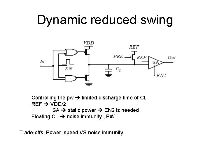
Dynamic reduced swing Controlling the pw limited discharge time of CL REF VDD/2 SA static power EN 2 is needed Floating CL noise immunity , PW Trade-offs: Power, speed VS noise immunity

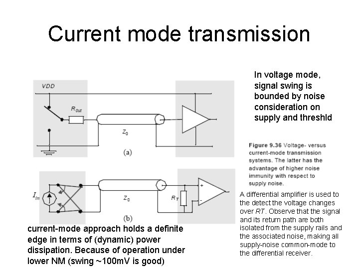
Current mode transmission In voltage mode, signal swing is bounded by noise consideration on supply and threshld current-mode approach holds a definite edge in terms of (dynamic) power dissipation. Because of operation under lower NM (swing ~100 m. V is good) A differential amplifier is used to the detect the voltage changes over RT. Observe that the signal and its return path are both isolated from the supply rails and the associated noise, making all supply-noise common-mode to the differential receiver.

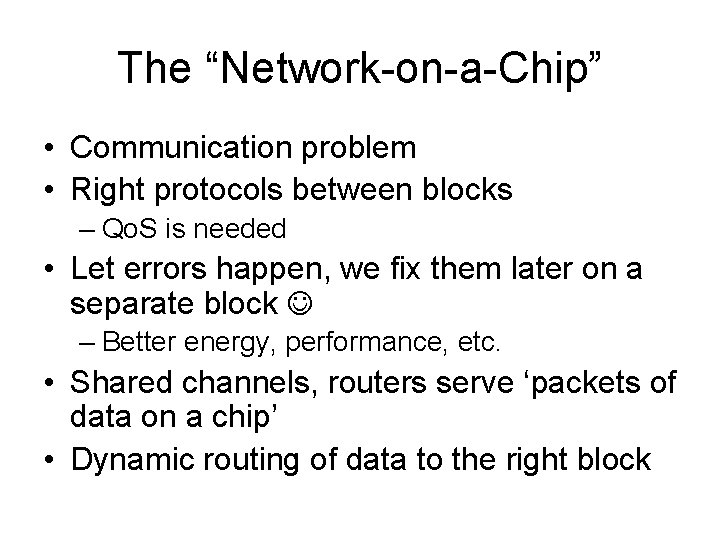
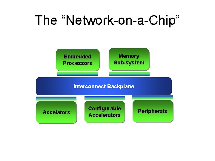
The “Network-on-a-Chip” • Communication problem • Right protocols between blocks – Qo. S is needed • Let errors happen, we fix them later on a separate block – Better energy, performance, etc. • Shared channels, routers serve ‘packets of data on a chip’ • Dynamic routing of data to the right block

The “Network-on-a-Chip” Embedded Processors Memory Sub-system Interconnect Backplane Accelators Configurable Accelerators Peripherals