Adiabatic Circuits Mohammad Sharifkhani Introduction Applying slow input

Adiabatic Circuits Mohammad Sharifkhani

Introduction • Applying slow input slopes reduces E below CV 2 • Useful for driving large capacitors (Buffers) • Power reduction > 4 for pad drivers (1 MHz) Dissipated E over R
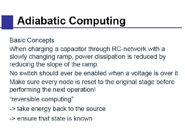

Basic concepts If we slow down the powerclock’s risetime by a factor of N: • The time required increases by a factor of N. • The current decreases by a factor of N. • The power decreases by a factor of N 2. • The dissipated energy per operation decreases by a factor of N. • The transferred charge and energy stored on Cap are unchanged. Denker 94 Regular Adia.
.")
Basic concepts • The output has a predetermined “resting” level (ground in this case). Whenever the output makes a transition away from the resting level, it must be returned (“recharged”) to the resting level before the start of the next calculation. This recharge step carries a terrible price. • Three ways to do the recharge: – Retractile cascade schemes – Memory Scheme – Reverse function

Retractile scheme • The input to stage 1 must be valid for 2 M + 1 phases. • What’s worse is that the throughput is reduced by a factor of M or so, since no pipelining is possible.

Memory scheme

Memory Scheme Next stage

Reversible Functions • If we know the prior state of the node. If the gate at stage m implements a logically reversible function the stage-m outputs to control the recharge of the stage-m inputs (F-1) • Not all functions are reversible extra computation might be neededs

Reversible Functions • Up to 8 phase clock is needed

An adder the three-bit reversible adder requires 20 times the number of devices and 32 times the area of a conventional adder using the same technology and laid out by the same designer. Athas 94 TVLSI
 ready (b) ready F 2 -1 internal ready (same as (a))")
Reversible Functions (a) ready (b) ready F 2 -1 internal ready (same as (a)) (a) recharged to VDD/2 1 - When one gate driving the other in Tri-state 2 - During the hand-off, the output of both gates are guaranteed to be the same VDD/2 F 1 out tied F 2 out tied Hand-off(F 2 -1 drives a, F 1 untie)

Rail driver ckt • Initial voltage of the rail : Vinint • Vfin is the target voltage • Cut the MOSFET when the peak voltage is reached (current is zero) • Off-chip inductor

Single phase/Memory based

Single phase/Memory based • Arbitrary logic functions are implementable • Auxiliary clock is needed

Single Pck + Reference Voltages Either MP 1 or MP 2 turns off Only the inputs set the IC at out, out_

SOURCE-COUPLED ADIABATIC LOGIC N or P current sources conducting

VDD+Vtn+Δ Adiabatic μP VDD+Vtn VDD Dynamically jumps up to more than VDD M 2 blocks the pull back energy-recovery latch (E-R latch)

Adiabatic μP : Two phase oscillator • Similar to what have been observed in LC tanks of RF circuits • For a constant capacitive load, the frequency will be stable and can be locked to a specific frequency with a varactor based phase-locked loop. • If synch with other blocks are needed: – We can use a FIFO and treat the adiabatic circuit as an asynch circuit

Adiabatic μP Large capacitive nodes

Adiabatic μP Domino style: When phi 2 is high, the middle gate is precharged already and can compute Same phase can not use PMOS precharge MOS fet higher than VDD is needed Precharged gates driven by E-R latches do not need protection n. FET’s in their pull-down stacks since the input signals are low during precharging. Combinatorial middle blocks Some energy in the tree can be recovered
- Slides: 21