Semiconductor Memories Mohammad Sharifkhani Outline Introduction Nonvolatile memories



![Yield curves at different stages of process maturity (from [Veendrick 92]) Yield curves at different stages of process maturity (from [Veendrick 92])](https://slidetodoc.com/presentation_image/4b7c7f56edaa8a68612e181513660bb5/image-78.jpg)
![Data Retention in DRAM From [Itoh 00] Data Retention in DRAM From [Itoh 00]](https://slidetodoc.com/presentation_image/4b7c7f56edaa8a68612e181513660bb5/image-85.jpg)
![1 Gbit Flash Memory From [Nakamura 02] 1 Gbit Flash Memory From [Nakamura 02]](https://slidetodoc.com/presentation_image/4b7c7f56edaa8a68612e181513660bb5/image-90.jpg)
![Semiconductor Memory Trends (updated) From [Itoh 01] Semiconductor Memory Trends (updated) From [Itoh 01]](https://slidetodoc.com/presentation_image/4b7c7f56edaa8a68612e181513660bb5/image-95.jpg)
![Trends in Memory Cell Area From [Itoh 01] Trends in Memory Cell Area From [Itoh 01]](https://slidetodoc.com/presentation_image/4b7c7f56edaa8a68612e181513660bb5/image-96.jpg)
- Slides: 97

Semiconductor Memories Mohammad Sharifkhani

Outline • Introduction • Non-volatile memories

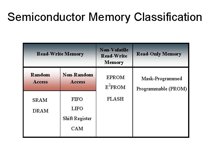
Semiconductor Memory Classification Read-Write Memory Random Access Non-Random Access SRAM FIFO DRAM LIFO Shift Register CAM Non-Volatile Read-Write Memory Read-Only Memory EPROM Mask-Programmed E 2 PROM Programmable (PROM) FLASH

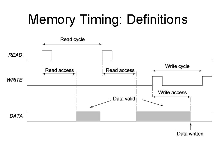
Memory Timing: Definitions

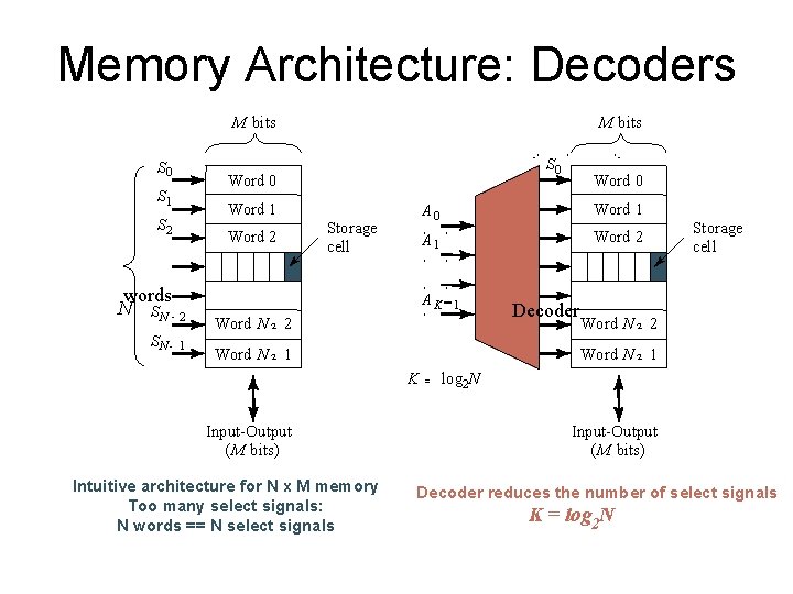
Memory Architecture: Decoders M bits S 0 Word 0 S 1 Word 1 S 2 Word 2 words N SN - 2 SN - M bits 1 Storage cell A 0 Word 1 A 1 Word 2 AK Word N 2 2 Word 0 -1 Word N 2 1 Decoder Storage cell Word N 2 2 Word N 2 1 K = log 2 N Input-Output (M bits) Intuitive architecture for N x M memory Too many select signals: N words == N select signals Input-Output (M bits) Decoder reduces the number of select signals K = log 2 N

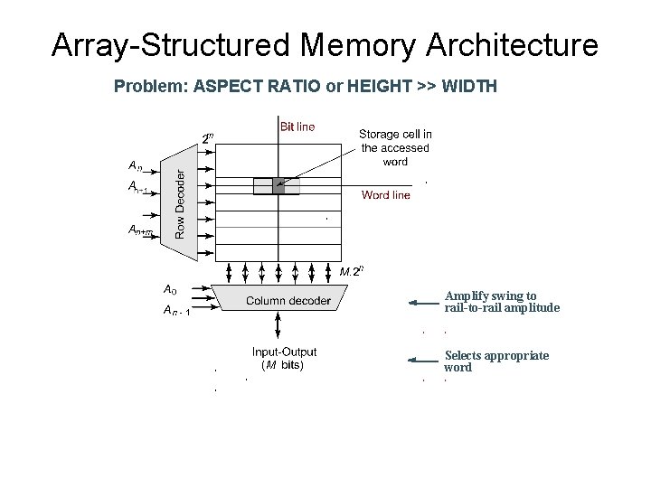
Array-Structured Memory Architecture Problem: ASPECT RATIO or HEIGHT >> WIDTH Amplify swing to rail-to-rail amplitude Selects appropriate word

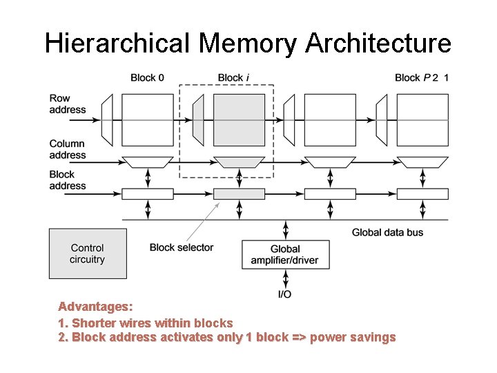
Hierarchical Memory Architecture Advantages: 1. Shorter wires within blocks 2. Block address activates only 1 block => power savings

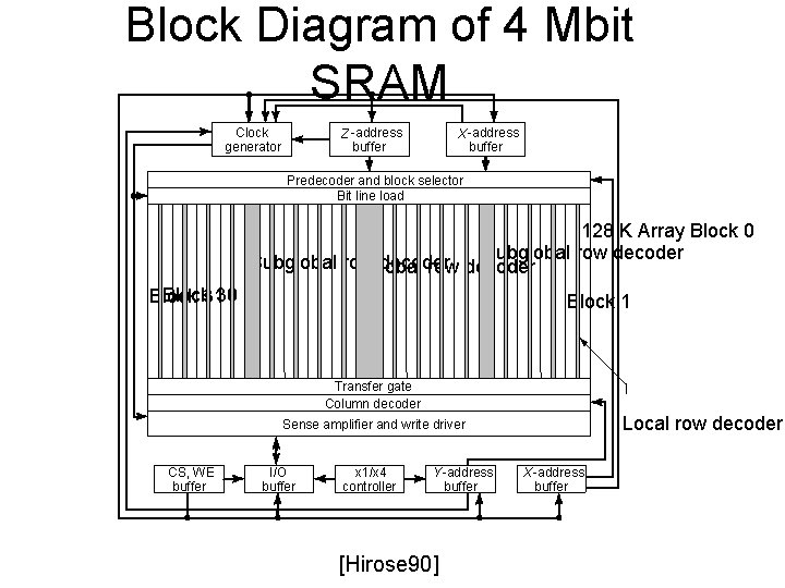
Block Diagram of 4 Mbit SRAM Clock generator Z-address buffer X-address buffer Predecoder and block selector Bit line load 128 K Array Block 0 Subglobal row decoder Subglobal row. Global decoder row decoder Block 3130 Block 1 Transfer gate Column decoder Local row decoder Sense amplifier and write driver CS, WE buffer I/O buffer x 1/x 4 controller Y-address buffer [Hirose 90] X-address buffer

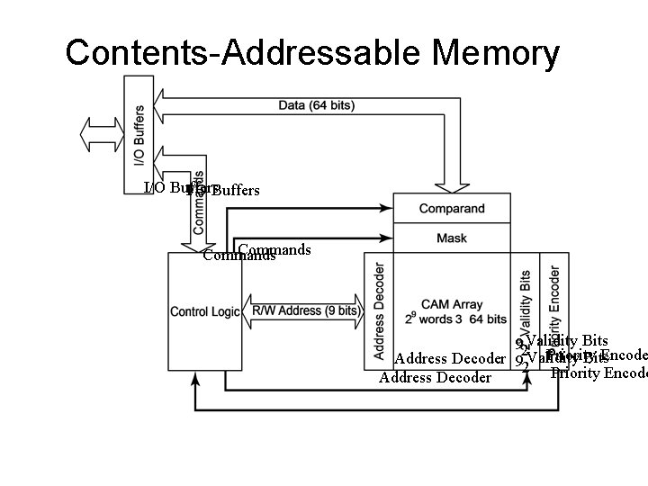
Contents-Addressable Memory I/O Buffers Commands 92 Validity Bits Priority Encode Bits Address Decoder 9 Validity 2 Priority Encode Address Decoder

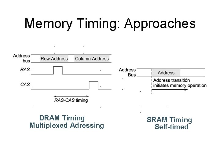
Memory Timing: Approaches DRAM Timing Multiplexed Adressing SRAM Timing Self-timed

• Introduction • Non volatile memories

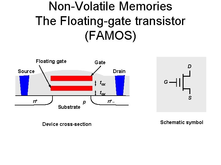
Non-Volatile Memories The Floating-gate transistor (FAMOS) Floating gate Gate Source D Drain G tox n+ Substrate p Device cross-section n+_ S Schematic symbol

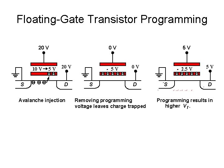
Floating-Gate Transistor Programming 20 V 10 V S 5 V 0 V 20 V D Avalanche injection - 5 V S 5 V 0 V D Removing programming voltage leaves charge trapped - 2. 5 V S 5 V D Programming results in higher V T.

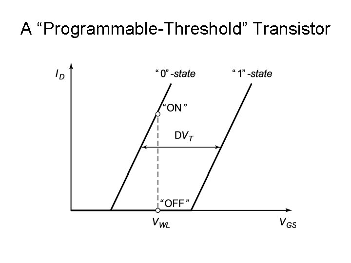
A “Programmable-Threshold” Transistor

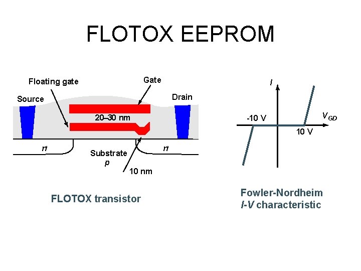
FLOTOX EEPROM Gate Floating gate I Drain Source 20– 30 nm V GD -10 V n 1 Substrate p 10 nm FLOTOX transistor Fowler-Nordheim I-V characteristic

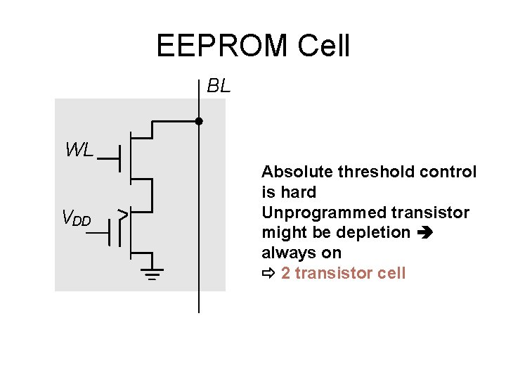
EEPROM Cell BL WL VDD Absolute threshold control is hard Unprogrammed transistor might be depletion always on 2 transistor cell

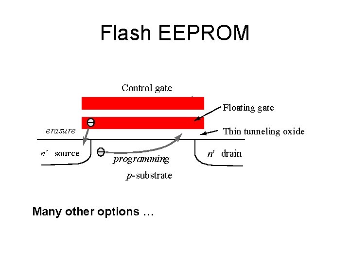
Flash EEPROM Control gate Floating gate erasure n 1 source Thin tunneling oxide programming p-substrate Many other options … n 1 drain

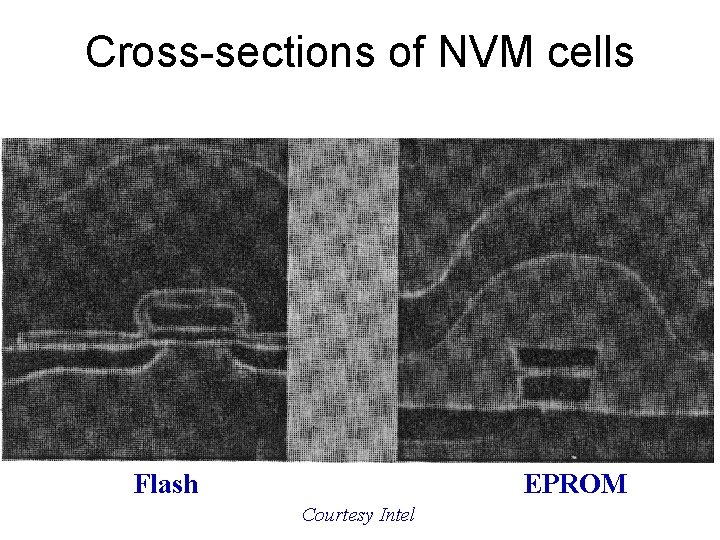
Cross-sections of NVM cells Flash EPROM Courtesy Intel

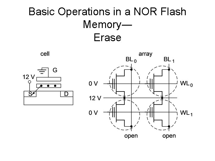
Basic Operations in a NOR Flash Memory― Erase

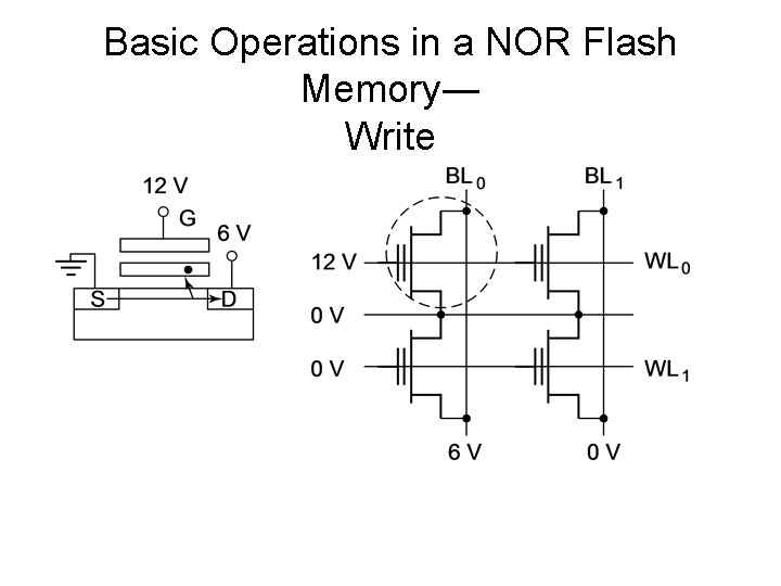
Basic Operations in a NOR Flash Memory― Write

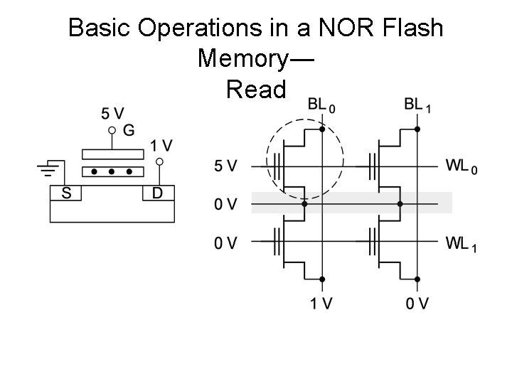
Basic Operations in a NOR Flash Memory― Read

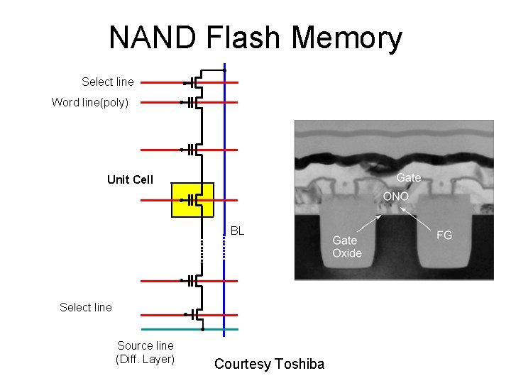
NAND Flash Memory Select line Word line(poly) Unit Cell BL Select line Source line (Diff. Layer) Courtesy Toshiba

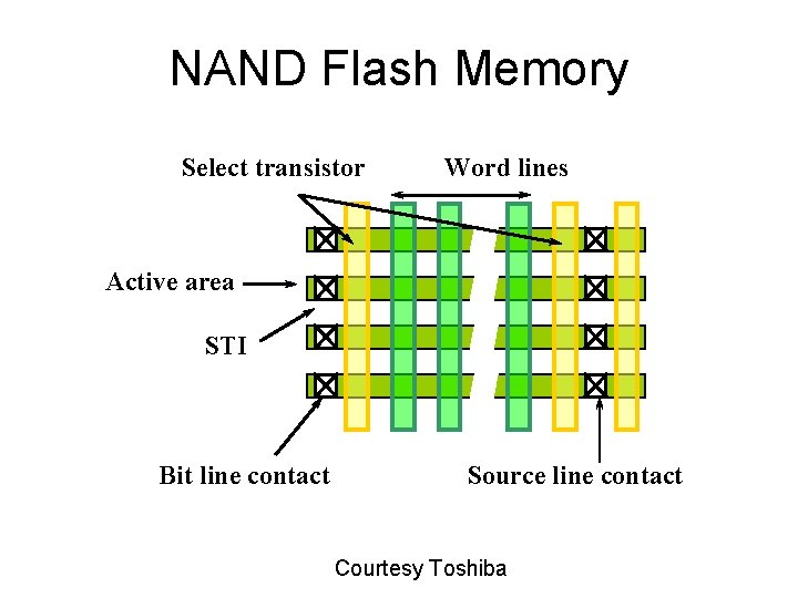
NAND Flash Memory Select transistor Word lines Active area STI Bit line contact Source line contact Courtesy Toshiba

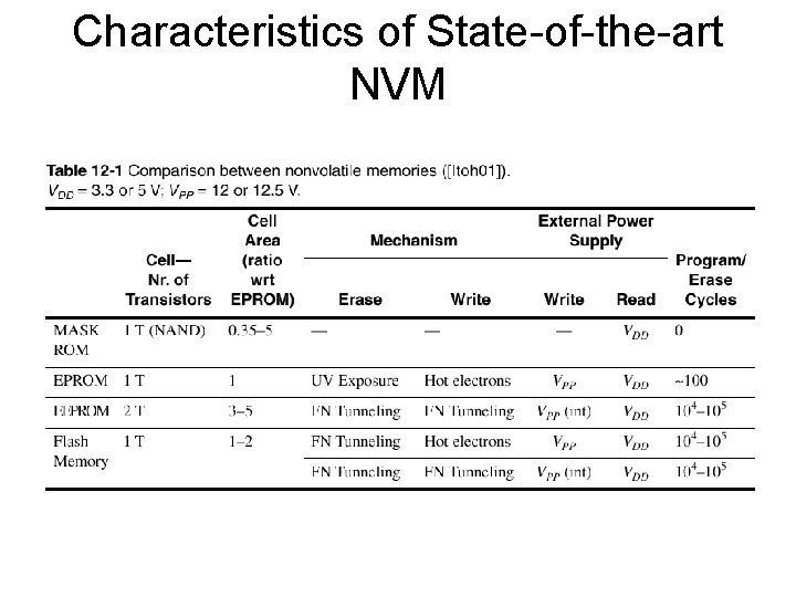
Characteristics of State-of-the-art NVM

Outline • Introduction • Non-volatile memories • RAM

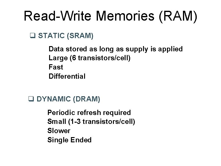
Read-Write Memories (RAM) q STATIC (SRAM) Data stored as long as supply is applied Large (6 transistors/cell) Fast Differential q DYNAMIC (DRAM) Periodic refresh required Small (1 -3 transistors/cell) Slower Single Ended

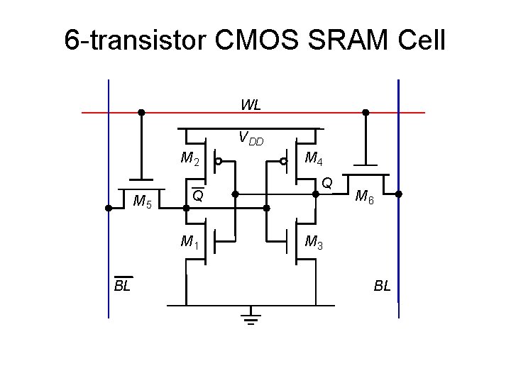
6 -transistor CMOS SRAM Cell WL V DD M 2 M 5 Q M 1 BL M 4 Q M 6 M 3 BL

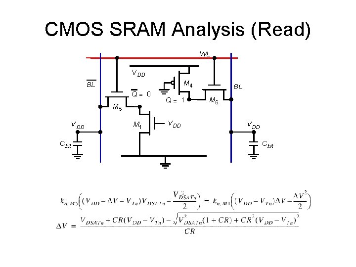
CMOS SRAM Analysis (Read) WL V DD M 4 BL Q= 0 M 5 V DD Cbit M 1 Q= 1 V DD BL M 6 V DD Cbit

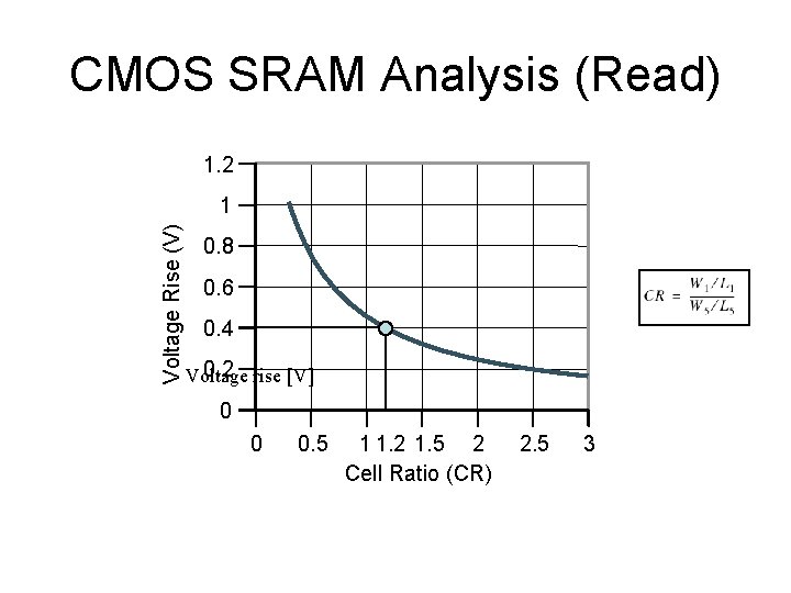
CMOS SRAM Analysis (Read) 1. 2 Voltage Rise (V) 1 0. 8 0. 6 0. 4 0. 2 rise [V] Voltage 0 0 0. 5 1 1. 2 1. 5 2 Cell Ratio (CR) 2. 5 3

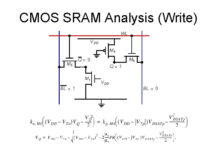
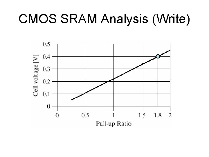
CMOS SRAM Analysis (Write) WL V DD M 4 M 5 Q= 1 M 1 BL = 1 M 6 Q= 0 V DD BL = 0

CMOS SRAM Analysis (Write)

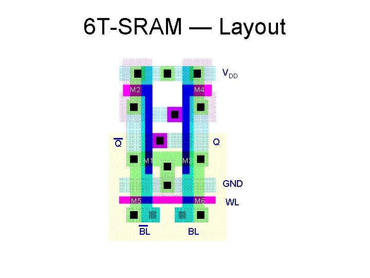
6 T-SRAM — Layout VDD M 2 M 4 Q Q M 1 M 3 GND M 5 BL M 6 BL WL

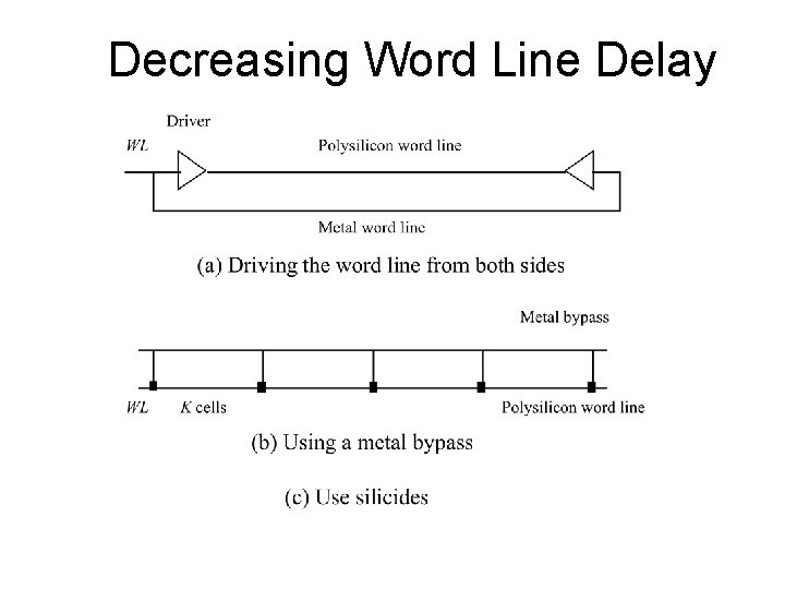
Decreasing Word Line Delay

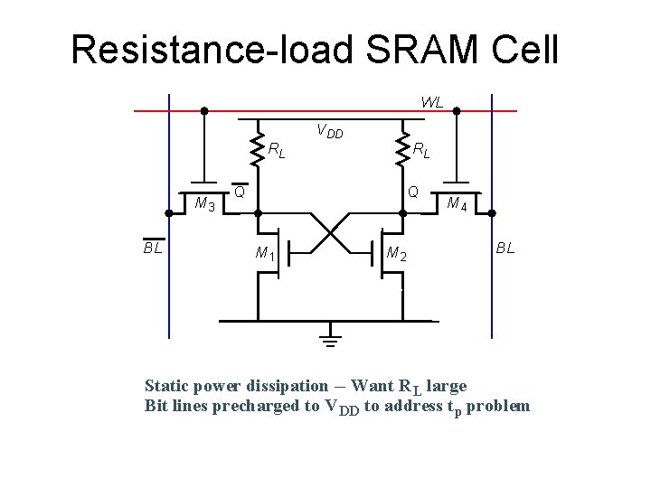
Resistance-load SRAM Cell WL RL M 3 BL V DD RL Q Q M 1 M 2 M 4 BL Static power dissipation -- Want R L large Bit lines precharged to V DD to address t p problem

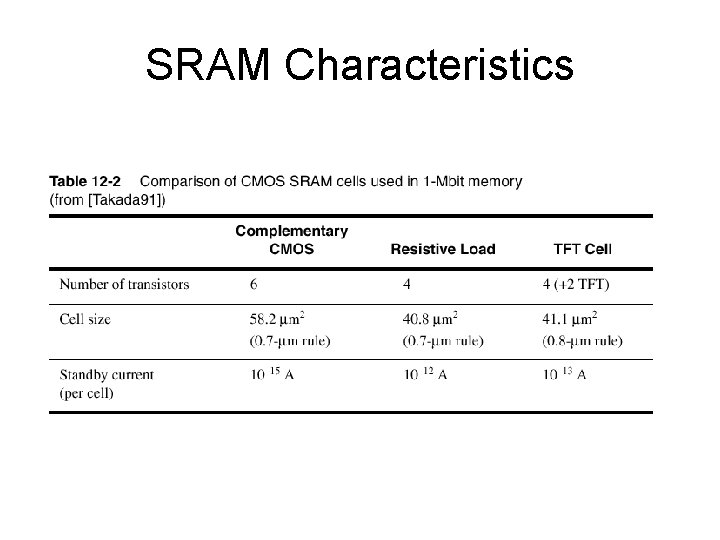
SRAM Characteristics

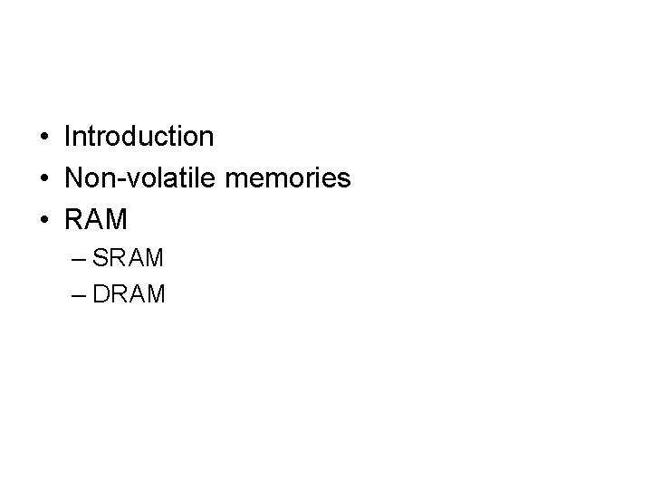
• Introduction • Non-volatile memories • RAM – SRAM – DRAM

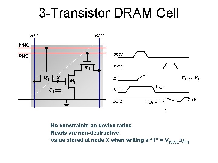
3 -Transistor DRAM Cell BL 1 BL 2 WWL RWL M 3 X M 1 CS M 2 RWL V DD 2 V T X BL 1 BL 2 V DD 2 V T No constraints on device ratios Reads are non-destructive Value stored at node X when writing a “ 1” = V WWL-VTn DV

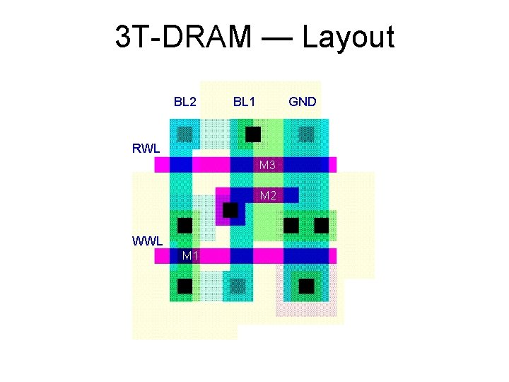
3 T-DRAM — Layout BL 2 BL 1 GND RWL M 3 M 2 WWL M 1

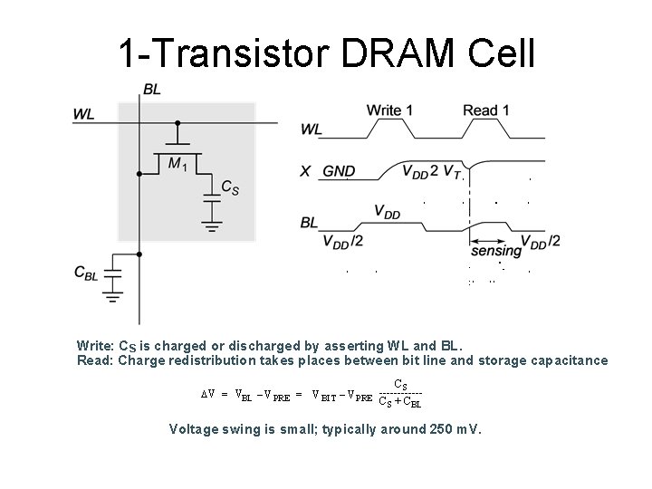
1 -Transistor DRAM Cell Write: C S is charged or discharged by asserting WL and BL. Read: Charge redistribution takes places between bit line and storage capacitance CS DV = VBL – V PRE = V BIT – V PRE ------C S + CBL Voltage swing is small; typically around 250 m. V.

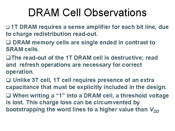
DRAM Cell Observations q 1 T DRAM requires a sense amplifier for each bit line, due to charge redistribution read-out. q DRAM memory cells are single ended in contrast to SRAM cells. q. The read-out of the 1 T DRAM cell is destructive; read and refresh operations are necessary for correct operation. q Unlike 3 T cell, 1 T cell requires presence of an extra capacitance that must be explicitly included in the design. q When writing a “ 1” into a DRAM cell, a threshold voltage is lost. This charge loss can be circumvented by bootstrapping the word lines to a higher value than VDD

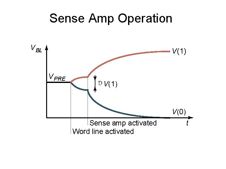
Sense Amp Operation V BL V(1) V PRE D V(1) V(0) Sense amp activated Word line activated t

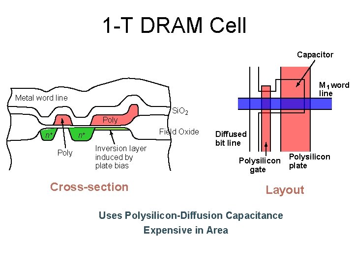
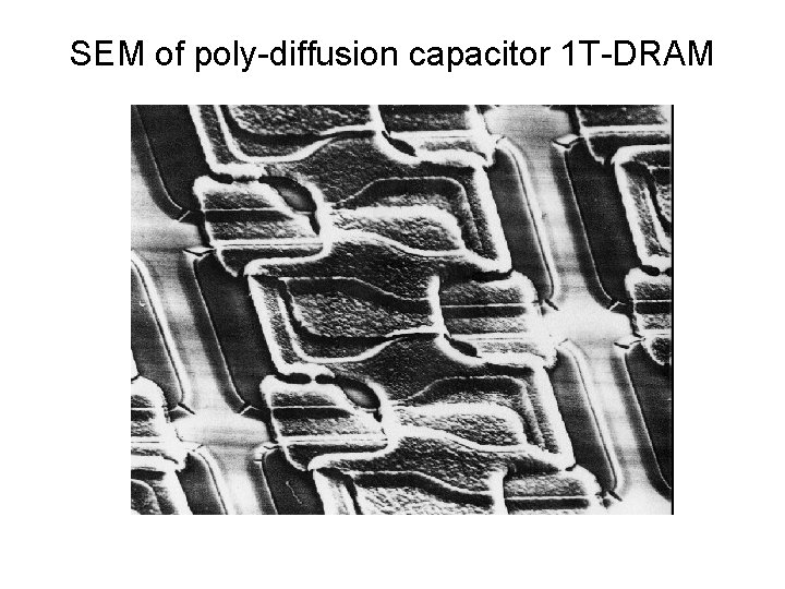
1 -T DRAM Cell Capacitor M 1 word line Metal word line Poly n+ Field Oxide n+ Poly Si. O 2 Inversion layer induced by plate bias Cross-section Diffused bit line Polysilicon gate Polysilicon plate Layout Uses Polysilicon-Diffusion Capacitance Expensive in Area

SEM of poly-diffusion capacitor 1 T-DRAM

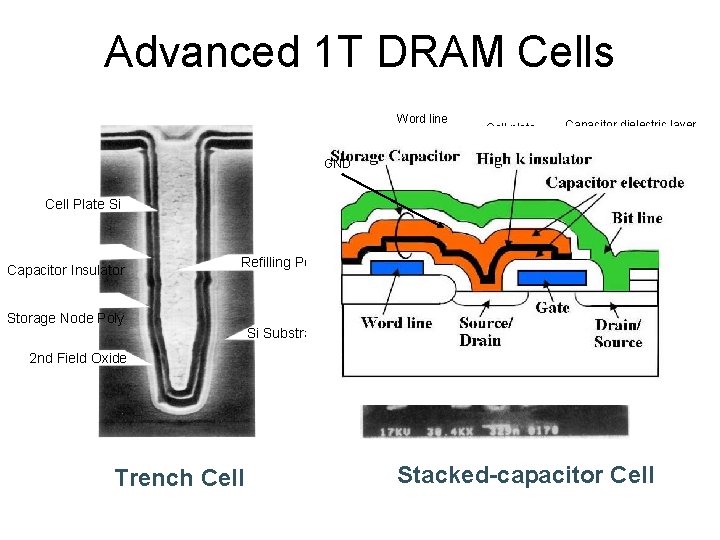
Advanced 1 T DRAM Cells Word line Insulating Layer Cell plate Capacitor dielectric layer GND Cell Plate Si Capacitor Insulator Refilling Poly Storage Node Poly Transfer gate Isolation Storage electrode Si Substrate 2 nd Field Oxide Trench Cell Stacked-capacitor Cell

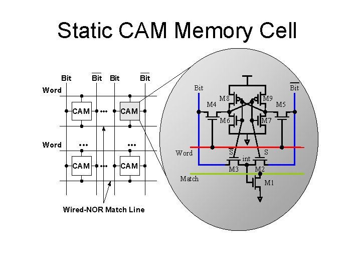
Static CAM Memory Cell Bit Bit Bit Word CAM Word • • • CAM • • • M 4 CAM • • • Word CAM M 8 M 9 M 6 M 7 S M 3 Match Wired-NOR Match Line Bit int S M 2 M 1 M 5

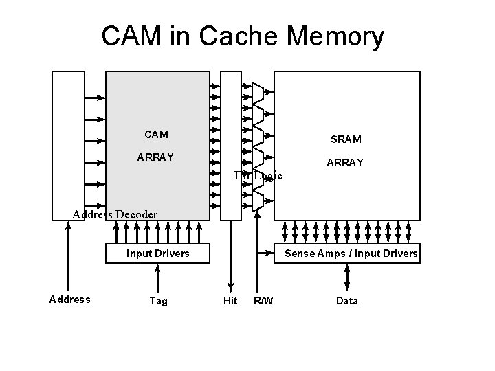
CAM in Cache Memory CAM SRAM ARRAY Hit Logic Address Decoder Input Drivers Address Tag Sense Amps / Input Drivers Hit R/W Data

• • Introduction Non-volatile memories RAM Periphery circuits

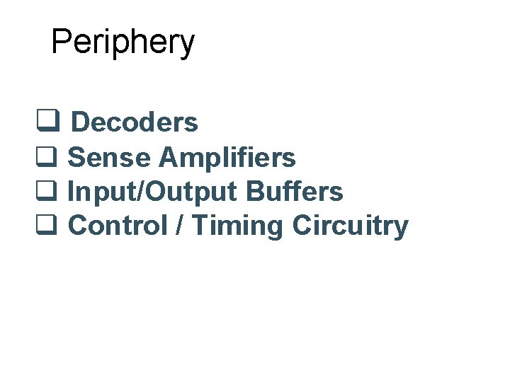
Periphery q Decoders q Sense Amplifiers q Input/Output Buffers q Control / Timing Circuitry

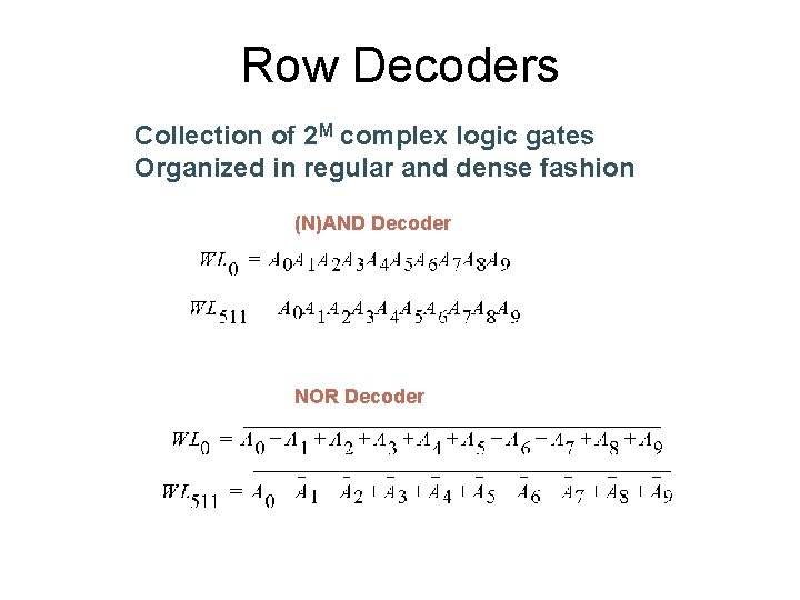
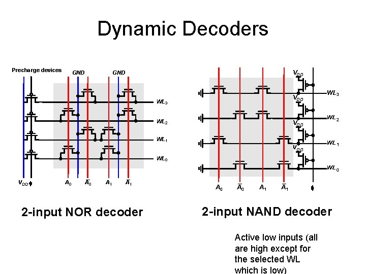
Row Decoders Collection of 2 M complex logic gates Organized in regular and dense fashion (N)AND Decoder NOR Decoder

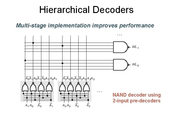
Hierarchical Decoders Multi-stage implementation improves performance • • • WL 1 WL 0 A 0 A 1 A 2 A 3 • • • A 1 A 0 A 1 A 3 A 2 A 3 NAND decoder using 2 -input pre-decoders

Dynamic Decoders Precharge devices GND VDD GND WL 3 VDD WL 3 WL 2 VDD WL 1 V DD WL 0 VDD f A 0 A 1 2 -input NOR decoder A 0 A 1 f 2 -input NAND decoder Active low inputs (all are high except for the selected WL which is low)

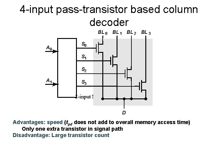
4 -input pass-transistor based column decoder BL 0 BL 1 BL 2 BL 3 A 0 S 1 S 2 A 1 S 3 2 -input NOR decoder D Advantages: speed (tpd does not add to overall memory access time) Only one extra transistor in signal path Disadvantage: Large transistor count

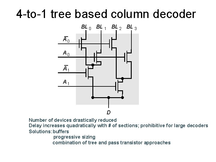
4 -to-1 tree based column decoder BL 0 BL 1 BL 2 BL 3 A 0 A 1 D Number of devices drastically reduced Delay increases quadratically with # of sections; prohibitive for large decoders Solutions: buffers progressive sizing combination of tree and pass transistor approaches

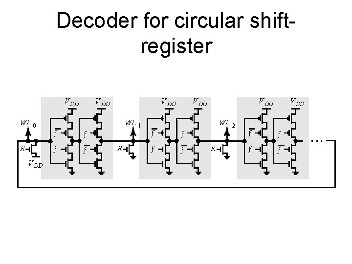
Decoder for circular shiftregister V DD WL 0 f R f V DD f R V DD WL 1 f f V DD f f 2 f f R V DD f f f • • •

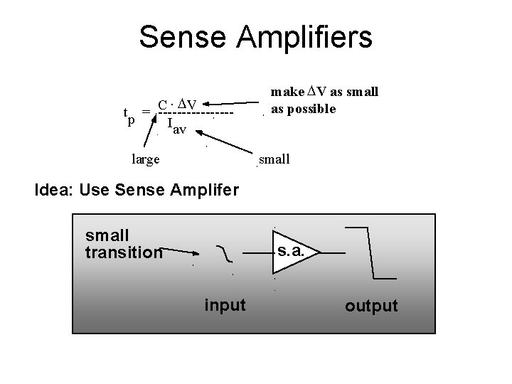
Sense Amplifiers × DV C tp = --------Iav large make D V as small as possible small Idea: Use Sense Amplifer small transition s. a. input output

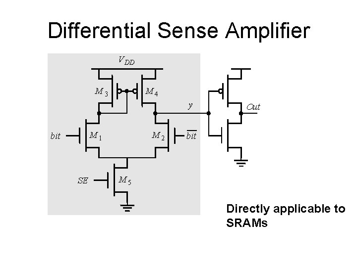
Differential Sense Amplifier V DD M 3 M 4 y M 1 bit SE M 2 Out bit M 5 Directly applicable to SRAMs

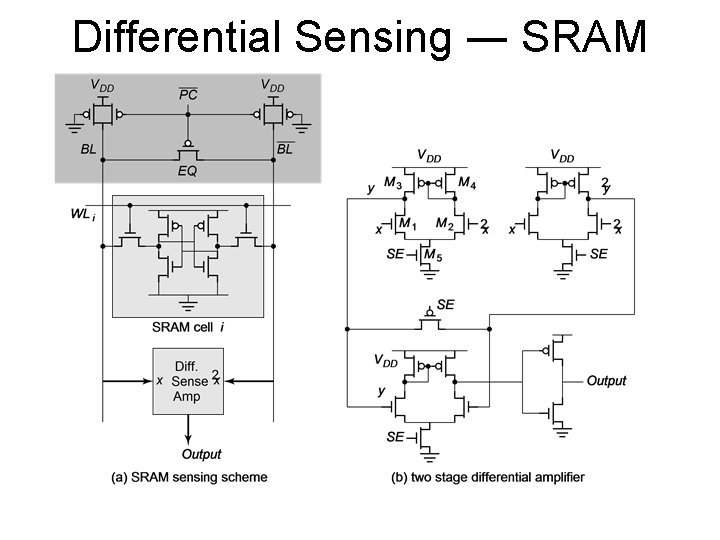
Differential Sensing ― SRAM

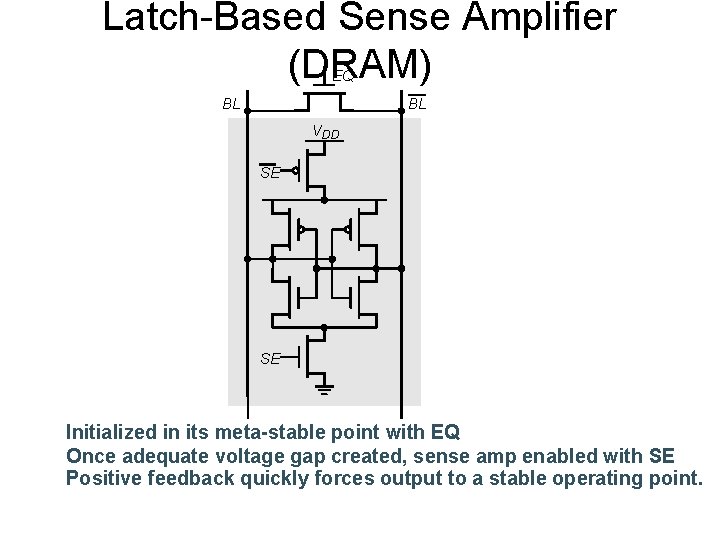
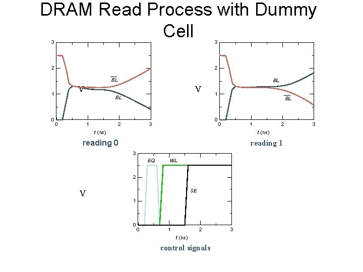
Latch-Based Sense Amplifier (DRAM) EQ BL BL VDD SE SE Initialized in its meta-stable point with EQ Once adequate voltage gap created, sense amp enabled with SE Positive feedback quickly forces output to a stable operating point.

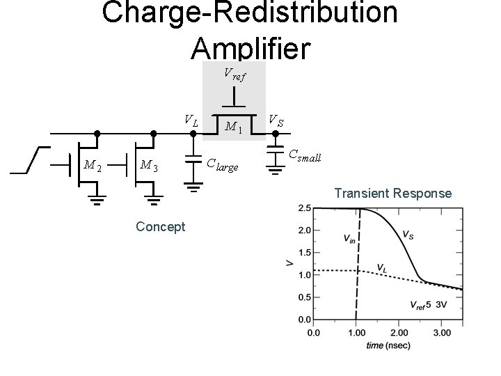
Charge-Redistribution Amplifier V ref VL M 2 M 3 M 1 C large VS C small Transient Response Concept

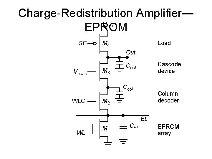
Charge-Redistribution Amplifier― V EPROM DD SE Load M 4 Out V casc M 3 Cascode device Cout Ccol WLC Column decoder M 2 BL WL M 1 CBL EPROM array

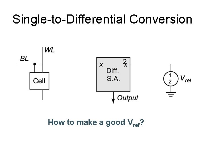
Single-to-Differential Conversion How to make a good Vref?

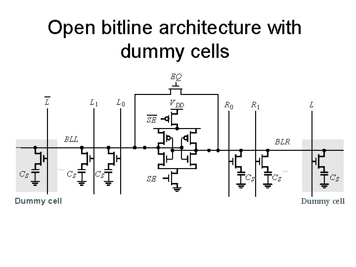
Open bitline architecture with dummy cells EQ L L 1 L 0 V DD R 0 R 1 L SE BLL CS … Dummy cell CS BLR CS SE CS CS … CS Dummy cell

DRAM Read Process with Dummy Cell 3 3 2 2 BL V 1 0 BL V BL 0 1 2 1 0 3 BL 0 1 t (ns) reading 0 reading 1 3 EQ WL 2 V 2 SE 1 0 0 1 2 t (ns) control signals 3 3

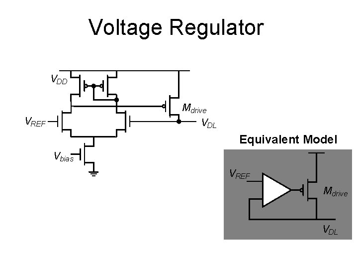
Voltage Regulator VDD Mdrive VDL VREF Equivalent Model Vbias VREF + Mdrive VDL

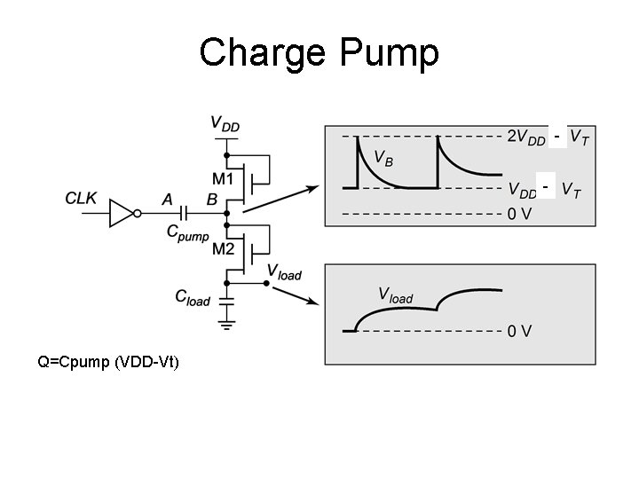
Charge Pump - Q=Cpump (VDD-Vt)

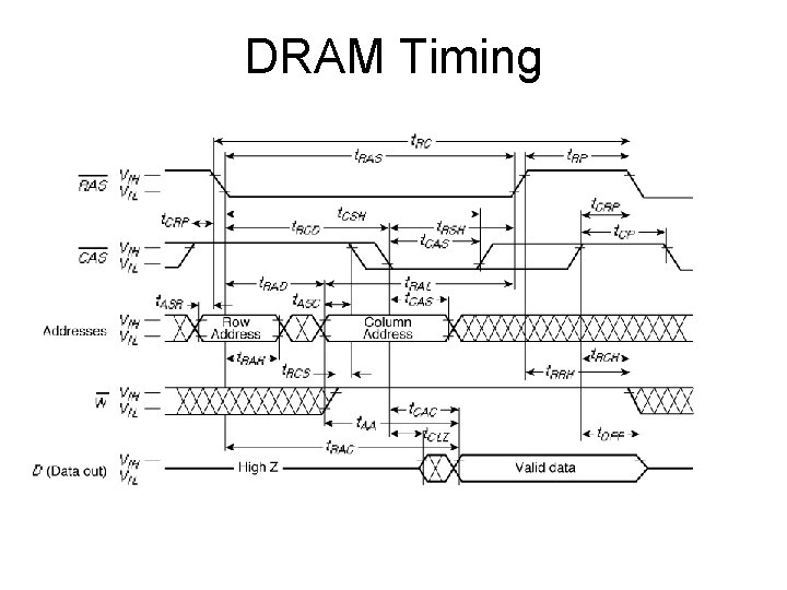
DRAM Timing

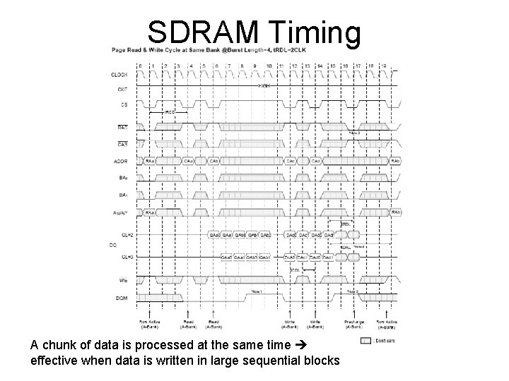
SDRAM Timing A chunk of data is processed at the same time effective when data is written in large sequential blocks

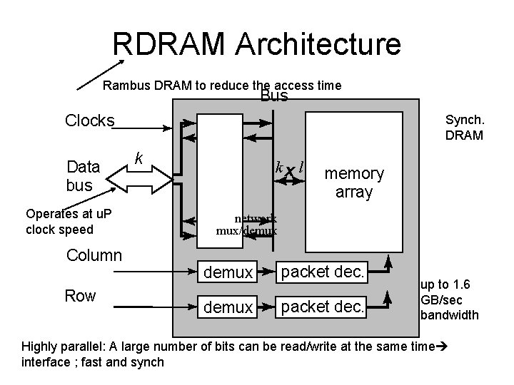
RDRAM Architecture Rambus DRAM to reduce the access time Bus Clocks Data bus Operates at u. P clock speed Column Row Synch. DRAM k kx l memory array network mux/demux packet dec. up to 1. 6 GB/sec bandwidth Highly parallel: A large number of bits can be read/write at the same time interface ; fast and synch

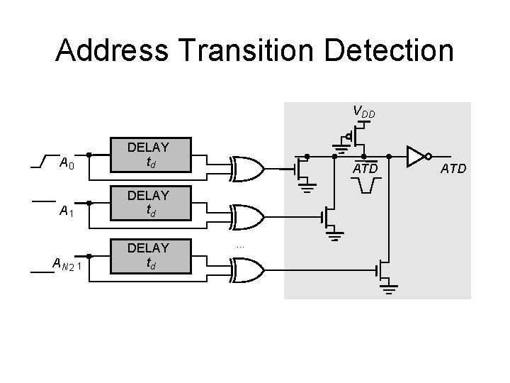
Address Transition Detection V DD A 0 DELAY td A 1 DELAY td A N 2 1 DELAY td ATD … ATD

• • • Introduction Non-volatile memories RAM Periphery Reliability

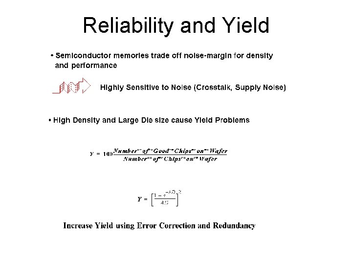
Reliability and Yield

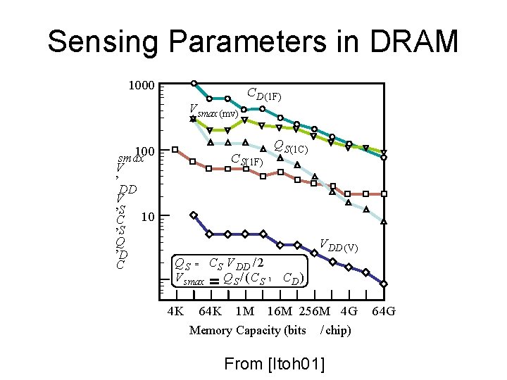
Sensing Parameters in DRAM 1000 V smax (mv) 100 smax V , DD V , S 10 C , S Q , D C C D(1 F) C S(1 F) Q S(1 C) V DD (V) Q S = C S V DD / 2 V smax = Q S / (C S 1 C D ) 4 K 64 K 1 M 16 M 256 M 4 G Memory Capacity (bits / chip) From [Itoh 01] 64 G

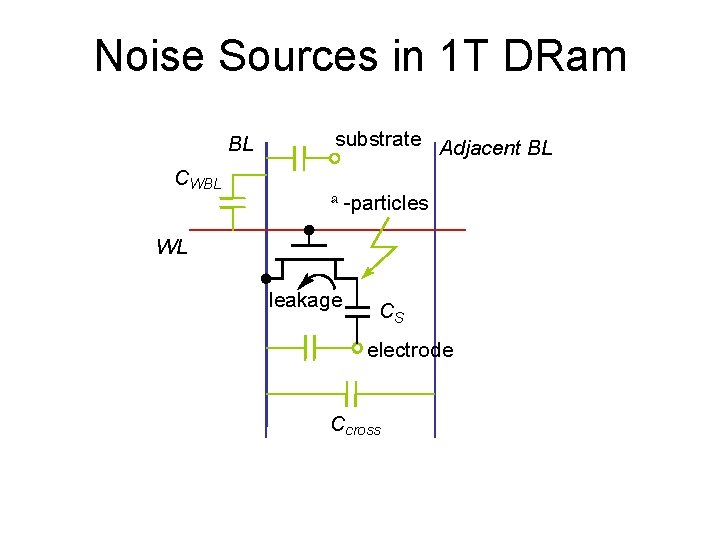
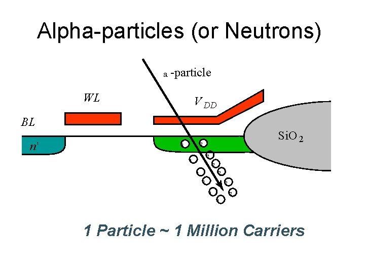
Noise Sources in 1 T DRam BL CWBL substrate Adjacent BL a -particles WL leakage CS electrode Ccross

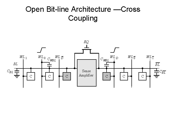
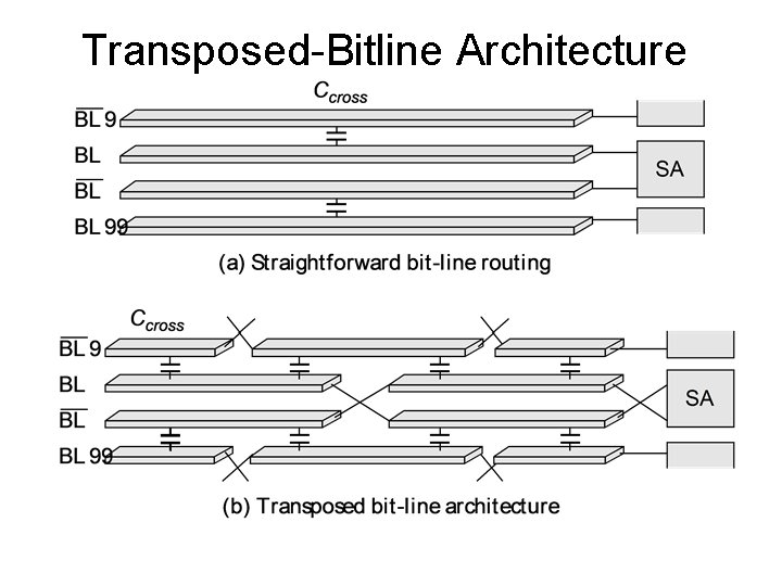
Open Bit-line Architecture —Cross Coupling EQ WL 1 WL 0 BL WL C WBL D C WBL WL D WL 1 WL 0 BL C C C Sense Amplifier C BL C C C

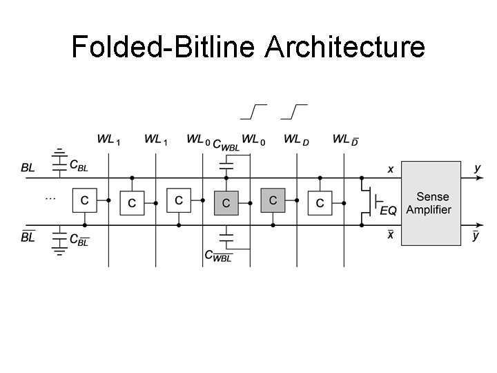
Folded-Bitline Architecture

Transposed-Bitline Architecture

Alpha-particles (or Neutrons) a -particle WL V DD BL n 1 Si. O 2 2 1 2 1 Particle ~ 1 Million Carriers
![Yield curves at different stages of process maturity from Veendrick 92 Yield curves at different stages of process maturity (from [Veendrick 92])](https://slidetodoc.com/presentation_image/4b7c7f56edaa8a68612e181513660bb5/image-78.jpg)
Yield curves at different stages of process maturity (from [Veendrick 92])

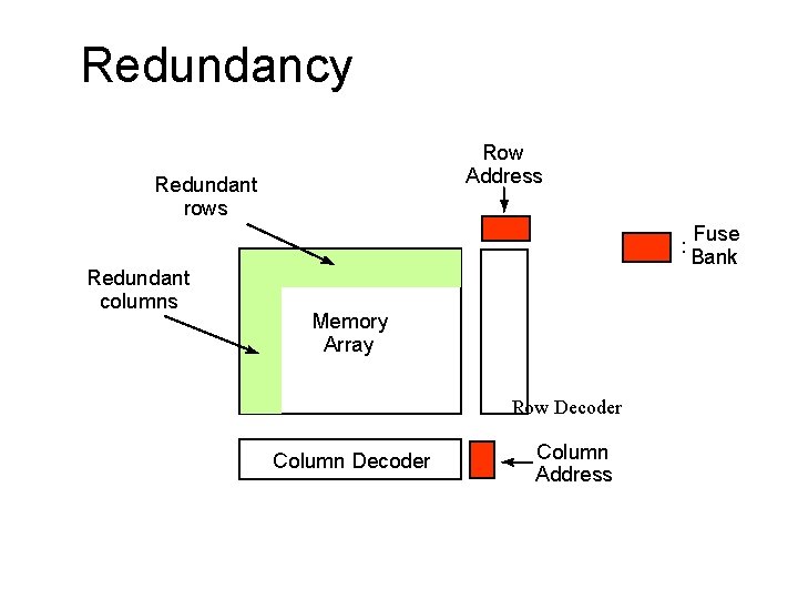
Redundancy Row Address Redundant rows : Redundant columns Memory Array Row Decoder Column Address Fuse Bank

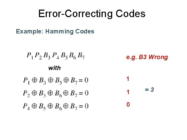
Error-Correcting Codes Example: Hamming Codes e. g. B 3 Wrong with 1 1 0 =3

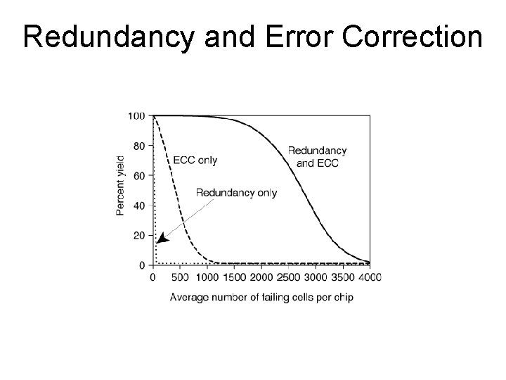
Redundancy and Error Correction

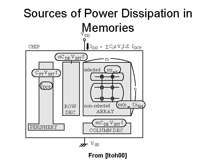
Sources of Power Dissipation in Memories V DD I DD = Σ C iΔ V if+Σ I DCP CHIP n. C DE V INT f m selected C PT V INT f mi act I DCP n ROW DEC PERIPHERY m(n 1)i hld non-selected ARRAY m. C DE V INT f COLUMN DEC V SS From [Itoh 00]

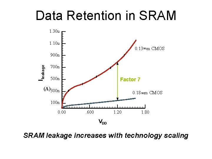
Data Retention in SRAM 1. 30 u 1. 10 u 0. 13 m m CMOS Ileakage 900 n 700 n 500 n Factor 7 (A)300 n 0. 18 m m CMOS 100 n 0. 00 . 600 1. 20 1. 80 VDD SRAM leakage increases with technology scaling

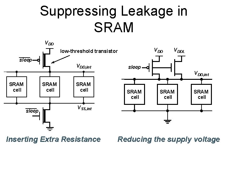
Suppressing Leakage in SRAM V DD low-threshold transistor V DDL sleep V DD, int SRAM cell sleep SRAM cell V SS, int Inserting Extra Resistance Reducing the supply voltage
![Data Retention in DRAM From Itoh 00 Data Retention in DRAM From [Itoh 00]](https://slidetodoc.com/presentation_image/4b7c7f56edaa8a68612e181513660bb5/image-85.jpg)
Data Retention in DRAM From [Itoh 00]

Case Studies • SRAM • Flash Memory

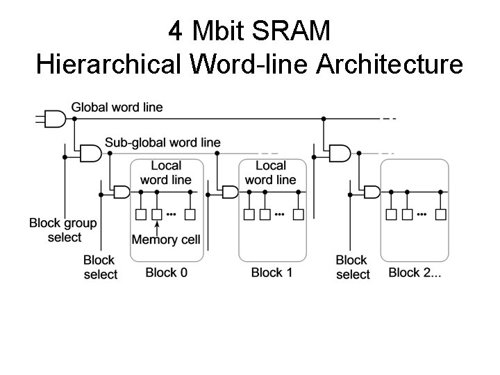
4 Mbit SRAM Hierarchical Word-line Architecture

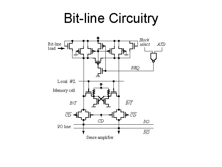
Bit-line Circuitry Block select Bit-line load BEQ Local WL Memory cell B /T CD CD CD I/O line I/O Sense amplifier ATD

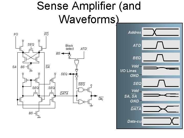
Sense Amplifier (and Waveforms) I /O Address I /O SEQ Block select ATD BS BEQ SA BS Vdd I/O Lines GND SA SEQ SEQ SEQ DATA Dei Vdd SA, SA GND DATA BS Data-cut
![1 Gbit Flash Memory From Nakamura 02 1 Gbit Flash Memory From [Nakamura 02]](https://slidetodoc.com/presentation_image/4b7c7f56edaa8a68612e181513660bb5/image-90.jpg)
1 Gbit Flash Memory From [Nakamura 02]

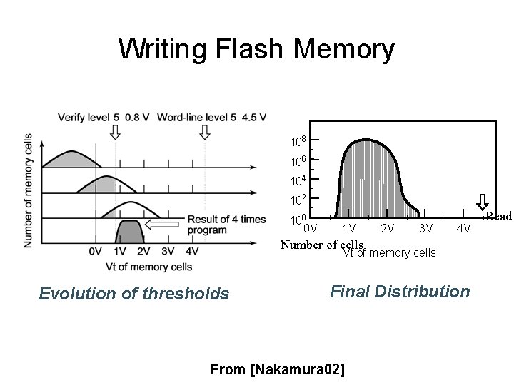
Writing Flash Memory 108 106 104 102 100 0 V 1 V 2 V 3 V 4 V Number of cells Vt of memory cells Evolution of thresholds Final Distribution From [Nakamura 02] Read

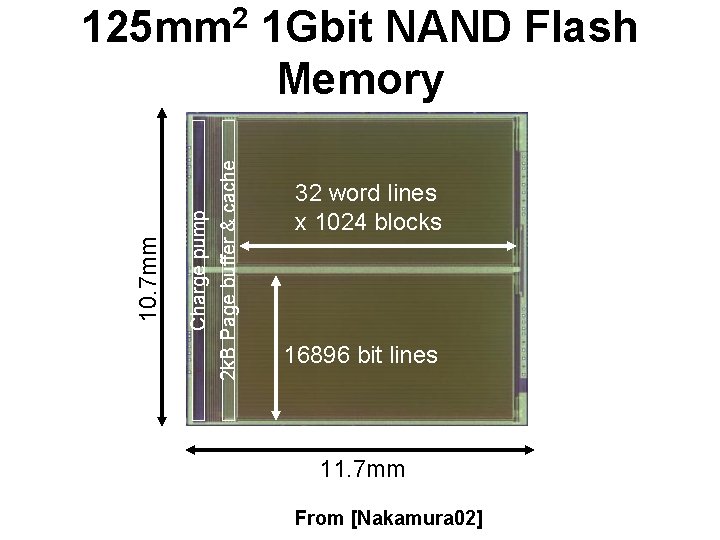
Charge pump 2 k. B Page buffer & cache 10. 7 mm 125 mm 2 1 Gbit NAND Flash Memory 32 word lines x 1024 blocks 16896 bit lines 11. 7 mm From [Nakamura 02]

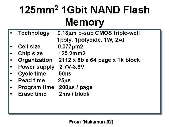
2 125 mm • • • 1 Gbit NAND Flash Memory Technology 0. 13 m p-sub CMOS triple-well 1 poly, 1 polycide, 1 W, 2 Al Cell size 0. 077 m 2 Chip size 125. 2 mm 2 Organization 2112 x 8 b x 64 page x 1 k block Power supply 2. 7 V-3. 6 V Cycle time 50 ns Read time 25 s Program time 200 s / page Erase time 2 ms / block From [Nakamura 02]

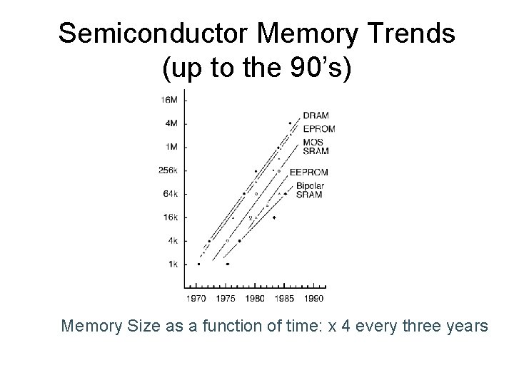
Semiconductor Memory Trends (up to the 90’s) Memory Size as a function of time: x 4 every three years
![Semiconductor Memory Trends updated From Itoh 01 Semiconductor Memory Trends (updated) From [Itoh 01]](https://slidetodoc.com/presentation_image/4b7c7f56edaa8a68612e181513660bb5/image-95.jpg)
Semiconductor Memory Trends (updated) From [Itoh 01]
![Trends in Memory Cell Area From Itoh 01 Trends in Memory Cell Area From [Itoh 01]](https://slidetodoc.com/presentation_image/4b7c7f56edaa8a68612e181513660bb5/image-96.jpg)
Trends in Memory Cell Area From [Itoh 01]

Future generations • Very specialized technologies for stand alone memories expensive • Reliability is going to be a very important issue (SER) particularly for SRAMs and DRAMs • Power is going to be the limiting factor particularly when it comes to standby currents • Embedded memories is the prominent market thrust driven by all mobile/So. C applications